
Nanowires: Technology, Physics and Perspectives
Institute for Semiconductor Nanoelectronics and Jülich Aachen Research Alliance Forschungszentrum Jülich, D-52425 Jülich, Germany
1. Introduction
Nanowires (NWs) are currently considered as strong contenders to provide possible solutions in several areas of semiconductor research, including the integration of III-V compounds on Si, the ultimate scaling of CMOS devices, high speed and low power circuitry (“green transistor”), and the realization of quantum information technology. This versatility of NWs has attracted the attention of numerous research groups studying their fabrication and characterization. However, even though substantial progress has been made in recent years, including the demonstration of many device prototypes, some of the fundamental NW physics is not yet fully understood in areas as varied as NW nucleation, structural, transport and optical properties.
Silicon NWs are grown typically either by the vapor-liquid-solid (VLS) mechanism using Au particles as catalyst1-3 or are fabricated by nanolithography.4 The latter approach makes it possible to carve NWs into strained Si,5 leading to uniaxially strained structures. The NW can be wrapped with a surrounding gate, providing optimized control of the transistor channel due to improved electrostatics compared to planar CMOS technology. Further, the NW technology may enable us to integrate novel transistor concepts, like Schottky barrier transistors or tunnel transistors,6,7 to optimize carrier injection, speed and power consumption. Nanopatterned Si substrates have great potential in serving as compliant templates for the growth of III-V nanostructures. The nanoscale footprint provided by these templates can accommodate a large lattice mismatch by elastic deformation.
Indium-rich III/V nanowires, namely In(Ga)N, In(Ga)As and In(Ga)Sb NWs, are of particular interest due to their high electron mobility and low effective mass. The latter leads to the observation of quantum effects in reasonably “large” NWs.8 These In-rich NWs have the peculiarity that the Fermi level at the surface is pinned within the conduction band, leading to metallic behavior in the conductivity for narrow wires, with an electron gas at the circumference. Indeed, magnetotransport investigations reveal pronounced oscillations in the conductivity periodic in magnetic flux. These are explained by the contribution of coherent circular quantum states along the surface of the nanowires. However, little is known about the shape of the potential in these In-rich nanowires and its dependence on the doping level and the diameter of the nanowire.
Finally, the large surface to volume ratio in NWs leads to a strong impact of surface scattering on the mobility. Thus, the mobility reported in In-rich nanowires falls short compared to quantum well or even bulk structures. Possible solutions are core/shell structures providing a well-defined clean interface for electron confinement. First experiments performed using MOVPE-grown GaAs/AlGaAs core/shell structures will be discussed. The introduction of lateral and vertical heterointerfaces while growing the nanowires are envisioned as a first step to exactly control the growth and positioning of quantum dots. Ultimately, this route may provide a suitable concept for quantum information processing.
2. Silicon nanowires
We have fabricated silicon NW devices using a top-down approach. A fairly standard process has been employed, using e-beam lithography to define the wire, followed by reactive ion etching (RIE) for the nanowire mesa. Next the gate stack is formed using either a SiO2/poly-Si gate stack or a high-κ dielectric film combined with a matching metallic layer. Finally, source and drain contacts are implanted and metallized. Figure 1 shows a scanning electron microscopy (SEM) image of a long channel device fabricated using a strained Si-on-insulator (SSOI) layer. Long-channel devices were fabricated to accurately determine the impact of strain on the mobility of charge carriers in the channel. To estimate the strain in the Si nanowire carved into an SSOI layer, finite element simulations of the strain in suspended Si NWs have been performed. It is obvious that the strain perpendicular to the NW axis (x-direction in Fig. 2 (left)) is released due to plastic deformation, whereas the strain parallel to the axis (y-direction in Fig. 2 (left)) is expected to remain, i.e. the wire is stretched between the source and drain contacts, leading to a uniaxial strain within the Si wire.
The contour plots show the results of the finite element calculations for wires with different aspects ratios, i.e. wire height vs. wire width in x-direction, ranging from 8 to 32.5 Figure 2 (right) shows that for the x-component a small compressive strain is found, whereas strong tensile strain persists along the Si wire.
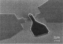
Figure 1. SEM image of a Si nanowire FET with a top gate.
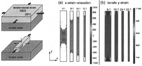
Figure 2. Illustration of the strain relaxation for Si nanowires fabricated from strained SOI layers.
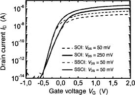
Figure 3. Comparison of I(VG) characteristics at fixed VDS of Si NW devices fabricated from strained and unstrained SOI layers (L = 3 μm for all devices).
The calculations indicate that the strong uniaxial strain along the Si NW axis should lead to reduced electron effective mass and thus enhanced electron mobility. To study the impact of the strain, devices have been fabricated from both SSOI and unstrained SOI substrates. Figure 3 shows the I(V) characteristics of both types of devices processed using the same parameters.
The devices have a 3 μm long channel and are measured under a source-drain voltage VDS of 50 (dashed lines) and 250 mV (solid lines). For both conditions, the saturation current increases by a factor of 2.5 for strained devices compared to unstrained devices. This result clearly indicates that the incorporated strain in the Si channel is substantially larger than that observed for mechanically bent Si NW transistors9 and exceeds 1 GPa as indicated in the model calculation presented in Fig. 2 (right).
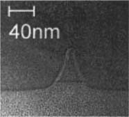
Figure 4. Cross sectional TEM ¡mage of a Si nanowire fabricated on SSOI.
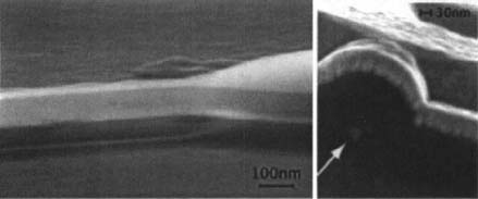
Figure 5. SEM images of freestanding Si nanowire (left) and circular nanowire after several oxidation and etching cycles (right).
Short-channel devices were fabricated from 50 nm thick SSOI layers. Devices having a gate length LG = 0.2 μm show a nearly ideal subthreshold slope of 62 mV/dec and excellent ION/IOFF ratios exceeding 107 at VDS = 250 mV. Figure 4 shows a cross-sectional TEM micrograph of the channel, which has a triangular shape with the gate wrapping the sidewalls of the device. Further improvements can be expected for devices with an all-around gate. For this purpose, wires with a rectangular cross-section have been freed from the substrate and transformed into a wire with a circular cross-section, as shown in Fig. 5, using repeated oxidation and etching steps. The optimized electrostatics of a circular device with an all-around gate should lead to an even better ION/IOFF ratio.
The developed technology is suitable for the further integration of new device concepts and designs, in particular Schottky-MOSFETs6 and tunnel FETs.7 These concepts may allow modified carrier injection mechanisms that can overcome the 60 mV/dec limit for the subthreshold slope in standard FETs. Moreover, the quantization of the states in a nanowire might be beneficial for the increase of the saturation currents in a tunnel FET (TFET).
3. InN nanowires
Nitride nanowires can easily be grown by MBE on a Si substrate using appropriate growth conditions. Typically N-rich conditions are used to grow GaN10 as well as InN”NWs. The presence of nitrogen radicals released by the plasma cell leads to a formation of an amorphous SiNx layer at the Si surface. Despite this amorphous layer, crystalline nanowires with the c-axis perpendicular to the substrate surface nucleate on Si (111). Moreover, for GaN NWs even a thick amorphous SiO2 layer does not hamper the wire formation.12 Here we discuss the InN NWs deposited on Si (111), which exhibit a surface accumulation layer. The Fermi level is pinned about 0.8-0.9 eV above the conduction band edge,13 leading to a pronounced band bending and a cylindrical accumulation layer containing an electron gas along the wire surface. The situation is depicted in Fig. 6. The conduction band edge with the corresponding electron wavefunctions are calculated by solving the coupled Poisson and Schrödinger equations in cylindrical coordinates using the effective mass approximation.
The calculations shown in Fig. 6 correspond to an InN nanowire with a diameter of 80 nm (radius r = 40 nm) and a surface state density of 1013 cm2. The Fermi level in the centre of the wire is slightly below the conduction band edge. These conditions lead to the filling of two subbands E1 and E2, with all carriers confined in the vicinity of the surface. The situation can be considered as a two-dimensional electron gas (2DEG) scrolled into a narrow tube. Due to strong band bending, the carrier confinement at the nanowire surface is very robust and present even in wires having a diameter less than 50 nm. The cylindrical 2DEG was analyzed by magnetotransport measurements with the magnetic field B both normal and parallel to the NW axis. For a B field parallel to the axis, the energy levels for the electrons are periodic in the magnetic field. The periodicity is given by the magnetic flux quantum Φ0 = h/e and consequently oscillations of the conductivity in dependence on magnetic flux14 are expected. Well-resolved oscillations in the resistivity as a function of B are indeed detected, with the periodicity of Φo/A, where A denotes the area of the cross-section of the wire. These oscillations persist up to a temperature of 30 K. The obtained data clearly indicate that the electrons move in a tubular 2DEG at the vicinity of the nanowire surface. At low bias voltages in the diffusive transport regime, the electrons walk randomly in the 2DEG, having a free mean path of lC between scattering events as well as a phase coherence length lΦ > lC defined by phase breaking scattering events, similar to planar 2DEG structures.15 Both quantities strongly depend on temperature due to phonon scattering. However, in nanostructures the dimensions L of the sample might be close to lΦ, leading to universal conductance fluctuations (UCFs) depending on a perpendicular magnetic field.16 These UCFs are most pronounced when the sample size and ΙΦ are similar. Accordingly, the rms(G) roughness of the UCF provides insight into the phase coherence length of the electrons in the diffusive regime:
![]()
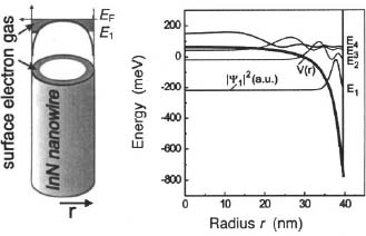
Figure 6. Schematic view of the surface enhancement layer in an InN NW and calculated profile of the conduction band V(r) and probability density for the lowest four subbands n = 1–4. The Fermi level is set to the zero of energy.
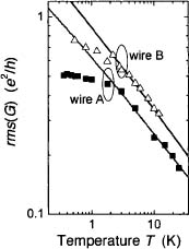
Figure 7. Root mean square of the universal magnetoconductance G oscillations vs. temperature T. For 7 < 2 K the amplitude saturates as the phase coherence length exceeds the wire length L
In Fig. 7, the temperature dependence of the rms roughness is plotted for two InN wires of different length L. The increase of the rms value as the temperature drops reflects the increase of lΦ with decreasing T. For both wires a saturation of the rms(G) value is found at low temperatures; at this point the lΦ value exceeds the length of the wire.17
The magnetotransport measurements reveal coherent quantum states in the InN nanowires, which might be attributed to the nearly perfect crystallinity and low surface defect density of the nanowires prepared by self-assembled MBE. Moreover, the low-temperature quantum transport properties of gated InN nanowires were investigated. A clear weak antilocalization effect18 was found in the averaged magnetoconductance indicating the presence of spin-orbit coupling.19 The latter effect is important for spin manipulation in nanoscale spintronic devices. The unexpected robustness of the weak antilocalization effect observed in narrow InN wires gives evidence that the tubular topology of the surface electron gas in InN nanowires is maintained also at very small dimensions.
4. InAs nanowires
Indium arsenide NWs were deposited by MBE on GaAs (111) wafers covered with very thin (~6 nm) layers of HSQ, a resist that forms a SiOx layer upon annealing. Such thin layers will exhibit a large density of pinholes, which act as nucleation points for NWs.20 It is speculated that in the first stage of growth, an In droplet forms in the depression of the pinhole. The wire starts to grow via the VLS growth mode, with the In droplet remaining on top of the growing wire. Figure 8 (left) shows an SEM image of the sample after deposition of InAs wires. Some multifaceted InAs clusters are found on the surface, next to the wires. It is unclear whether they grew on the SiOx surface or at pinholes of a size not suitable for wire growth. The InAs wires have a length of a few micros and diameters in the ~100 nm range. Astonishingly, they are rather uniform in size, which might support the assumption that only pinholes of suitable size lead to wire growth. The InAs have a pronounced faceting exhibiting [110] sidewalls, which can be clearly seen in the enlargement of a single wire in Fig. 8 (right).
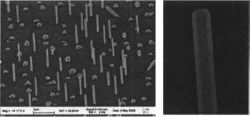
Figure 8. SEM images of MBE grown InAs nanowires on GaAs (111) substrates covered with a thin SiOx layer.
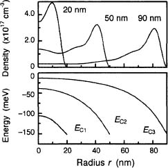
Figure 9. Calculated profile of the conduction band (lower curves) for three InAs NWs with 20, 50 and 90 nm radius and corresponding total electron densities (upper curves) as a function of radius.
In contrast to InN wires, the surface state density of InAs is lower and the Fermi level at an InAs surface is pinned only about 150 meV above the conduction band edge. Again a surface enrichment layer is formed leading to a tubular 2DEG at the surface of an undoped InAs nanowire. However, this 2DEG is much less confined and hence loses its clear 2D character at small diameters as compared to InN wires. The smaller pinning energy and the smaller electron mass lead to larger spreading of the electron wave function across the wire. As a result, the electron gas is transformed from a tubular 2DEG configuration to a quasi ID electron gas at a wire thickness below 50 nm.
This is illustrated in Fig. 9. The lower graph shows the conduction band edges EC1, EC2, and EC3 across the wire for three different wire radii r = 20, 50 and 90 nm, respectively. The Fermi energy is located at 0 meV in this illustration. The conduction band edge for the r = 20 nm is located more than 100 meV below the Fermi energy even in the centre of the wire, consequently the electron density (upper graph in Fig. 9) in the centre of the wire amounts to 3.5 x 1017 cm-3 for an undoped wire. Even though the maximum electron concentration in this wire is still tubular, a quasi one-dimensional transport can be expected. For larger wire diameters the tubular shape becomes more pronounced, however, even for a 180 nm wide nanowire the conduction band edge stays below the Fermi energy at the centre of the wire, making the entire wire degenerate. Consequently, undoped InAs nanowires are expected to have metallic properties, in particular the conductivity should increase with decreasing temperature. Experimentally it is found that the conductivity decreases, i.e. the resistance increases by approximately 30% with decreasing temperature, thus opposite to the predicted metallic behavior. Most likely, the carrier mobility of the electrons in these InAs wires is dominated by temperature-independent surface scattering. The increase in resistance of thin wires might be attributed to a decrease in carrier density at low temperatures caused by an activation energy dependence of electrons released by surface states. However, further studies are required to clarify this phenomenon. It should be noted, that Si-doped InAs wires show a pronounced reduction of their resistivity compared to undoped InAs wires. Furthermore the doped wires exhibit the expected metallic behavior, i.e. an increase of the resistance with temperature.
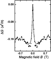
Figure 10. Averaged magnetoconductance G at low magnetic fields. Solid line represents the fit obtained by using Kettemann’s model.22
Magnetotransport measurements of thin InAs wires exhibit no signature of weak antilocalization. We attribute this finding to the predominantly one-dimensional transport properties within these wires. For InAs nanowires with a larger diameter, where the majority of the carriers is located in the tubular 2DEG configuration, quantum interference effects have been observed, similar to the results described above for the InN nanowires. The effective electric field in the tubular 2DEG due to the band bending leads to spin precession. Figure 10 shows the results of magnetotransport studies depicting the averaged conductivity G as a function of small B perpendicular to the wire axis. A clear peak at B = 0 is found, indicating weak antilocalization, i.e. spin precession leads to net destructive interference of backscattered electrons in a 2DEG.21
5. Conclusion
In this chapter we discussed the potential for semiconductor quantum wires for future nanoelectronics. Si NWs are a possible path to scale CMOS technology to its ultimate limits. The integration of novel device concepts, like Schottky barrier transistors or TFETs, modifying the carrier injection mechanisms to achieve ultra fast device switching frequencies are promising. However, to achieve high performance ID transport properties are crucial. Thus technological challenges to achieve Si wires with less than 7 nm diameter and controlled doping profiles, as well as appropriate source/drain and gate configurations, are quite serious.
Several paths for the fabrication of self-assembled III-V NWs grown without the use of a catalyst have been demonstrated. The possibility of growing such NWs on both III-V and Si substrates may allow future integration of opto-electronics on Si as well as advanced beyond-CMOS devices exploring spin as fundamental carrier of logic information.
References
1. A. M. Morales, C. M. Lieber, “A laser ablation method for the synthesis of crystalline semiconductor nanowires,” Science 279, 208 (1998).
2. T. Martensson, M. Borgstrom, W. Seifert, B. J. Ohlsson, and L. Samuelson, “Fabrication of individually seeded nanowire arrays by vapor-liquid-solid growth,” Nanotechnology 14, 1255 (2003).
3. H. J. Fan, P. Werner, and M. Zacharias, “Semiconductor nanowires: From self-organization to patterned growth,” Small 2, 700 (2006).
4. H. Sellier, G. P. Lansbergen, J. Caro, et al., “Subthreshold channels at the edges of nanoscale triple-gate silicon transistors,” Appl. Phys. Lett. 90, 073502 (2007).
5. S. F. Feste, J. Knoch, D. Buca, and S. Manti, “Fabrication of uniaxially strained silicon nanowires,” Thin Solid Films 517, 320 (2008).
6. M. Zhang, J. Knoch, J. Appenzeller, and S. Mantl, “Improved carrier injection in ultrathin-body SOI Schottky-barrier MOSFETs,” IEEE Electron Dev. Lett. 28, 223 (2008).
7. S. Saurabh and M. J. Kumar, “Impact of strain on drain current and threshold voltage of nanoscale double gate tunnel field effect transistor: Theoretical investigation and analysis,” Japan. J. Appl. Phys. 48, 064503 (2009).
8. A. Fuhrer, C. Fasth, and L. Samuelson, “Single electron pumping in InAs nanowire double quantum dots,” Appl. Phys. Lett. 91, 052109 (2007).
9. Y. J. Jeong, K. Miyaji, T. Saraya, and T. Hiramoto, “Silicon nanowire n-type metal-oxide-semiconductor field-effect transistors and single-electron transistors at room temperature under uniaxial tensile strain,” J. Appl. Phys. 105, 084514 (2009).
10. R. K. Debnath, R. Meijers, T. Richter, T. Stoica, R. Calarco, and H. Lüth, “Mechanism of molecular beam epitaxy growth of GaN nanowires on Si(111),”Appl. Phys. Lett. 90, 123117(2007).
11. R. Calarco and M. Marso, “GaN and InN nanowires grown by MBE: A comparison,” Appl. Phys. A 87, 499 (2007).
12. T. Stoica, E. Sutter R. J. Meijers, R. K. Debnath, R. Calarco, H. Lüth, and D. Grützmacher, “Interface and wetting layer effect on the catalyst-free nucleation and growth of GaN nanowires,” Small 4, 751 (2008).
13. V. N. Brudnyi, A. V. Kosobutsky, and N. G. Kolin, “The charge neutrality level and the Fermi level pinning in A(3)N (BN, AIN, GaN, InN) nitrides,” Russ. Phys. J. 51, 1270 (2008).
14. Th. Richter, Ch. Blömers, H. Lüth, R. Calarco, M. Indlekofer, and Th. Schäpers, “Flux quantization effects in InN nanowires,” Nano Lett. 8, 2834 (2008).
15. S. Washburn and R. A. Webb, “Quantum transport in small disordered samples from the diffusive to the ballistic regime,” Rep. Prog. Phys. 55, 1311 (1992).
16. Y. Ochiai, T. Onishi, M. Kawabe, K. Ishibashi, J. P. Bird, Y. Aoyagi, and T. Sugano, “Interference area of universal conduction fluctuations in narrow GaAs/AlGaAs wires,” Japan. J. Appl. Phys. 32, 528 (1993).
17. Ch. Blömers, Th. Schäpers, T. Richter, R. Calarco, H. Lueth, and M. Marso, “Temperature dependence of the phase-coherence length in InN nanowires,” Appl. Phys. Lett. 92, 132102 (2008).
18. G. Petersen, S. Estévez Hernández, R. Calarco, N. Demarina, and Th. Schäpers, “Spin-orbit coupling and phase-coherent transport in InN nanowires,” Phys. Rev. B 80, 125321 (2009).
19. Ζ. W. Jia, W. Z. Shen, H. Ogawa, and Q. X. Guo, “Electron dephasing in wurtzite indium nitride thin films,” Appl. Phys. Lett. 89, 232107 (2006).
20. S. Yoshida, I. Tamai, T. Sato, and H. Hasegawa, “Selective molecular beam epitaxy growth of GaAs hexagonal nanowire networks on (111)B patterned substrates,” Japan. J. Appl. Phys. 43, 2064 (2004).
21. S. Estevez Hernandez, M. Akabori, K. Sladek, et al, “Spin-orbit coupling and phase-coherence in short InAs nanowires,” submitted to Phys. Rev. B (2009).
22. S. Kettemann, “Dimensional control of antilocalization and spin relaxation in quantum wires,” Phys. Rev. Lett. 98, 176808 (2007).