
Fundamental Properties of Materials
4.1 Introduction
The properties of materials relevant to electrical engineering applications are mechanical, thermal and electromagnetic in nature. The mechanical properties which are of interest relate to the strength and deformation of materials, the latter being either reversible and governed by three elastic moduli or irreversible because of plastic changes or fracture. The thermal properties relate to heat capacity, conduction and expansion. The interaction of mechanical and thermal properties with the electrical properties leads to electromechanical and thermoelectric properties.
Traditionally, the electromagnetic properties are describable in terms of three main parameters: the electrical conductivity (σ), the magnetic permeability (μ), and the electric permittivity (ε). The relative magnitude of these parameters determines whether the material is, respectively, electrically conducting, magnetic or dielectric. The electromagnetic transmittance of the material (i.e. the optical transparency) is governed by the refractive index which may be complex in nature and thus lead to complicated electromagnetic behaviour.
4.2 Mechanical properties
The mechanical properties of materials relate to their strength, rigidity and ductility. Materials may be deformed elastically, by which it is meant that the deformation is reversible and that the stress (force per unit area) and resulting strain (fractional size change) are proportional (Hooke’s law). The constant of proportionality is known as the elastic modulus of which there are three types:
(1) Young’s modulus (M) relates tensile stress and strain;
(2) Shear modulus (G) relates shear stress and strain; and
(3) the bulk modulus (K) relates bulk stress and volume strain.
During elastic deformation, not only is there a longitudinal elongation but also a cross-sectional decrease. The ratio of longitudinal to transverse strain is Poisson’s ratio, γ.
If the materials are polycrystalline, the mechanical properties may be regarded as isotropic so that the four elastic constants may be interrelated by
The inherent strength of a material is limited by plastic deformation or fracture. Plastic deformation is a permanent deformation caused by a shearing of a few crystal planes (slip). Such deformation is affected by various types of dislocations within the material structure.
The fracture of a material is the separation into two or more parts by an applied stress and may be classified as either brittle or ductile. The former occurs after little or no plastic deformation, whereas ductile fracture occurs after extensive plastic deformation.
Materials may be strengthened but usually only at the expense of their ductility which may cause fabrication problems. Methods of increasing mechanical strength include work hardening (progressive application and removal of increasing stress), solution hardening (addition of an alloying element to produce internal strains), precipitation hardening (which involves careful heating and solution treatment), and dispersion hardening (diffusion of gases into the solid to produce hard particles).
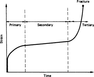
The stress and strain do not necessarily occur simultaneously in real materials but rather the material continues to deform indefinitely under the influence of a constant applied stress (creep). Such creep behaviour consists of four main phases (Figure 4.1). An initial instantaneous strain (which may be partly elastic and partly plastic) is followed by a primary creep region having a decreasing creep rate, a secondary creep region of constant minimum flow rate and a final region of accelerating strain ultimately leading to fracture.
4.3 Thermal properties
The basic thermal properties of materials include thermal capacity, conduction and expansion. The thermal capacity (the thermal energy required to raise the temperature by one degree Kelvin) is due to the storage of energy in the motion and oscillation of atoms and electrons. Such energy may be conducted through atomic and electronic collisions between regions at different temperatures. The thermal stability of the material is governed by the magnitudes of the thermal conduction and capacity since these parameters govern the temperature rise experienced by the material on the dissipation of power within the material. Such temperature rises can lead to technical difficulties, not only because of the eventual destruction of the material, but also due to its expansion which results from the increased amplitude of oscillation of the atoms.
4.4 Electrically conducting materials
Electrically conducting materials may be identified from fundamental electromagnetic theory as those for which the conduction current density jc is considerably greater than the displacement current density jd where
where D is the electric flux density.
For jc to dominate the electrical conductivity σ needs to be large. Since the electrical conductivity is approximately given by classical theory as
(where m and e are the electron mass and charge, respectively, and p is the mobility), a high concentration of conduction electrons (n) or a long time between collisions of electrons and the lattice ions of the material (2τc) leads to the dominance of jc.
Since both electrical and thermal conduction are due to the flow of electrons in metals, it should be anticipated that the electrical and thermal (K) conductivities should be related. The relationship is given by the Wiedemann—Franz law
where L is the Lorentz Number and T is the temperature.
This has implications for the removal of Joule heat (which depends upon σ) by thermal conduction (which depends upon K).
Furthermore, the conduction of heat may be accompanied by the flow of electric current. This flow ceases when opposed by the electric field created by the resulting charge migration. The electromotive force (e.m.f.) generated is characterised by the thermoelectric power s which is the potential difference (dv) per degree temperature difference (dT)
Thus the potential difference between the ends of a material with thermoelectric power S1 at different temperatures measured via junctions with a second material of thermoelectric power S2 is governed by (S1 − S2). This, the Seebeck effect, forms the basis of thermocouple operation. If, alternatively, a current is made to flow along or against a temperature gradient, the need for the conduction electrons to be in equilibrium with the crystal lattice leads to the heating of the cold end or the cooling of the hot end (Thompson effect), respectively. The flow of current through the junction between two materials can produce heating or cooling known as the Peltier effect, which can be used for temperature control.
The electrical conductivity of semiconductor materials incorporates both electrons (n−) and holes (u+) as carriers so that
In photoconductors the number of carriers n−, n+ is enhanced through the absorption of light energy to free the carriers for conduction.
For technical applications it is often preferred to use the reciprocal of conductivity, i.e. the resistivity, ρ. The resistivity of a pure, conventional conductor increases with temperature
where α is the temperature coefficient of resistivity (in parts per million per degree Celsius). The temperature dependence of the resistivity of some conductors is shown in Figure 4.2.
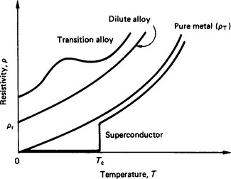
The resistivity of an impure conductor is greater than that of the pure conductor (due to additional electron collisions with the impurity ions) according to Matthiessen’s rule:
In the case of a dilute alloy (Nordheim’s rule)
where x is the impurity concentration.
However, for alloys of transition metals (e.g. nickel) the above rules do not apply. Instead the resistivity variation with temperature may possess a point of inflexion which has important implications for a temperature-independent resistivity over a limited range. Furthermore, some materials become superconducting below a critical temperature Tc whereby the resistivity decreases to zero. For such a superconducting state to be maintained the current density in the material needs to be kept below a critical value.
Under d.c. conditions the resistance of a bulk conductor depends on the cross-sectional area (A) and length (l)
With a.c. at an angular frequency ω the current conduction is confined to a peripheral annulus of effective width (skin depth)
where μ is the permeability, so that the effective cross-sectional area A is reduced and the resistance increases with signal frequency.
Electrical conduction in thin films is also governed by the proximity of the film surface contributing to the impedance of the electron flow
4.5 Magnetic materials
The magnetic influence of materials is incorporated in electromagnetic theory via the relative permeability which relates the magnetic flux density, B, to the magnetic field strength, H, according to
where μ0 is the permeability of free space for which μr = 1. A measure of the magnetic influence of a material is given by the magnetic susceptibility which is the difference between the relative permeability of the material and that of free space
However, in material science the preference is for the material influence to be described additively rather than factorially according to
where Jm is the magnetic moment per unit volume which is determined by the product of the magnetic moment of the elementary dipoles ![]() and their concentration N according to
and their concentration N according to
A number of physical processes may produce such elementary dipole moments and these determine the type of magnetism displayed by the material.
Diamagnetism occurs when the electron orbitals associated with the atoms of the material are distorted in the presence of an external magnetic field. The orbiting electrons may be regarded as forming circulating currents which, according to electromagnetic theory, have associated magnetic moments. On the application of a magnetic field the orbitals adjust to oppose the field. Diamagnetic susceptibility is temperature independent, of the order of 10−4 and is negative, implying a dilution of the magnetic flux within the material.
Paramagnetism is due to an inherent magnetic moment arising from an orbiting electron, a spinning electron and a spinning nucleus. In the latter two cases the magnetic moment may be regarded as originating from the spinning charge of the electron or proton constituting an effective circulating current. The nuclear effect is less pronounced than the electronic effect. Paramagnetic susceptibility is greater than diamagnetic susceptibility (ca. 10−3 to 10−4), is positive and decreases with temperature (T) according to the Curie law:
where C is the Curie constant.
Both diamagnetism and paramagnetism originate from the individual effects of atomic processes. However, in some materials, mainly the transition metals, the magnetic effects arising from individual atoms may be strongly coupled to give more pronounced magnetic properties to the bulk material. Such strong interatomic coupling leads to ferromagnetic, antiferromagnetic and ferrimagnetic effects
Ferromagnetism occurs when the magnetic moments of neighbouring atoms are aligned because of the strong interatomic coupling so that
where the suffixes A and B designate the neighbouring atoms. To minimise the magnetic energy of the bulk material, regions of like-magnetic-moment alignments (domains) are formed with neighbouring regions having differently orientated magnetic moments.
Antiferromagnetism occurs when the magnetic moments of neighbouring atoms are misaligned so that for a pure material the bulk magnetic effects are zero:
Ferrimagnetism arises when the neighbouring atoms in the misalignment have different magnetic moments so that there is a remnant magnetic effect in the bulk material:
For both ferromagnetic and ferrimagnetic materials the magnetic susceptibility is enhanced and considerably greater than for both diamagnetic and paramagnetic materials. In all cases the magnetic susceptibility decreases with temperature according to
where Tc is the Curie point for ferromagnetic materials and the Neel temperature for antiferromagnetic materials. The significance of Tc is that the material ceases to be strongly magnetic for temperatures above Tc and becomes instead paramagnetic in nature.
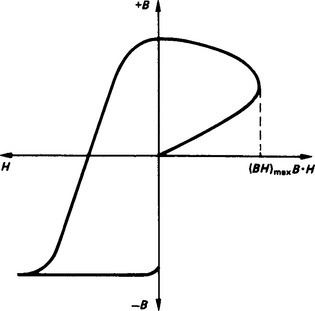
Incorporation of magnetic materials as part of devices in electrical networks (e.g. transformer cores), electronic circuits (e.g. magnetic pick-ups) or microwave systems (e.g. ferrite isolators) may produce power losses or waveform distortion. At power frequencies, the power losses are produced by hysteresis effects which arise from the inertia of the ferromagnetic domains in following changes in an applied magnetic field and which produces a hysteresis B—H loop (Figure 4.3). The power losses are given by the product of the energy product, the volume and the power frequency (energy product = (1/2BH)max). In addition, losses occur due to eddy currents flowing in the magnetic material. These depend on the resistivity of the material (ρ), the shape of the material (β), the dimension (d) perpendicular to the magnetic flux (B) and the power frequency (f) according to
Waveform distortion is produced by the non-linear relationship between B and H due to the hysteresis B—H loop because, according to Lenz’s law, the output voltage from an inductive element is given by
At radio and microwave frequencies, losses may occur due to the absorption of power from the electromagnetic wave to increase the energy of the elementary atomic magnetic dipoles. Ferrite materials which are used in radio and microwave frequency devices are anisotropic in nature so that the relative permeability is replaced by a permeability tensor.
Materials which demonstrate superconductivity do so not only below a critical temperature, Tc, and critical current density, but also below a critical magnetic field strength (Hc) which varies with temperature T according to
where Hc0 is the critical field at absolute zero of temperature.
For field strengths below Hc, superconductors become diamagnetic, implying a low magnetic flux density within the material (Figure 4.4). The transition to the diamagnetic state may occur abruptly at Hc (corresponding to type I superconductors which are pure materials) or more gradually (corresponding to type II superconductors which are more common and include impure materials).
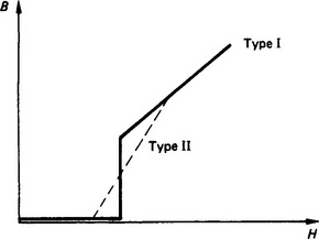
The ratio of the field penetration into the material (the London penetration depth, Λ) to the growth in superconductivity (the coherence length, ξ), which is known as the Ginsburg—Landau constant, determines whether a material is of type I (Λ/ξ < 0.71) or type II (Λ/ξ > 0.71). In type II superconductors, in particular, the growth in current density may lead to ‘flux jumping’ whereby flux lines are dislodged leading to power dissipation which causes heating and hence loss of superconduction.
4.6 Dielectric materials
In electromagnetism, dielectric properties are incorporated via the relative permittivity εr which relates the electric flux density, D, to the electric field strength, E, according to
where ε0 is the permittivity of free space against which the permittivity of a dielectric is normalised. Thus, since for free space εr = 1, the magnitude of dielectric effects may be considered in terms of the dielectric susceptibility
Alternatively, a relationship between D and E which is often preferred in fundamental materials studies is
where P is the polarisation per unit volume and
where p is the dipole moment of each atomic/molecular dipole, N is their concentration, EL is the local field within the dielectric which results from the electrostatic fields between ions and electrons
and α is the polarisability which is produced by a number of atomic or molecular processes in the dielectric material.
Electronic polarisation (αe) is produced when the electron orbital is distorted by the presence of an electric field (Figure 4.5(d)).
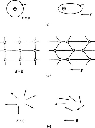
Figure 4.5 (a) Electronic polarisation (αe). (b) Ionic polarisation (αi). (c) Orientational polarisation (αo)
Ionic polarisation (αi) is produced when the lattice structure of the material is distorted by the electric field (Figure 4.5(b)).
Orientational polarisation αo arises when electric dipoles already exist in the dielectric and are re-aligned by an applied electric field (Figure 4.5(c)).
Other polarisation mechanisms which occur in some materials under special conditions are ion-jump polarisation and space charge polarisation (αs).
Consequently, the total polarisation per unit volume is
The electromagnetic and materials descriptions are interrelated via the Clausius—Mosotti equation:
For situations in which the electric field is time varying in a periodic manner the polarisation P may lag behind the field E due to the inertia associated with the physical processes described above. As a result, the relative permittivity becomes dependent on the E field angular frequency ω and on the relaxation time (τ) governing the inertia of the polarisation. As a result, the permittivity is complex in nature
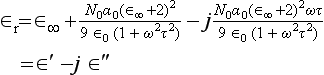
Since the relaxation times of the space charge and orientational polarisations differ significantly, the effects lead to sequential changes in ε′ and ε″ as the E field frequency increases. Ionic and electronic polarisation are governed by resonant effects (see Section 4.8) which also produce frequency-dependent complex permittivities (Figure 4.6).
Figure 4.6 Variation of real and imaginary parts of the permittivity. (IR–infra-red; r.f.–radiofrequency)
Since the velocity of propagation of an electromagnetic wave depends upon ε′,
the frequency dependence can lead to dispersion and waveform distortion. The imaginary component of εr leads to signal attenuation and power dissipation which accounts for the loss tangent of a capacitor
The permittivity of a dielectric composed of two components whose individual permittivities, ε1 and ε2, are not excessively different is given by
where χ1 is the fractional volume concentration of the ε1 component; m = 1 or − 1 depending upon whether the components are in parallel or series, respectively. For a random distribution of components such as in ceramics
The behaviour of anisotropic dielectrics requires the introduction of a susceptibility matrix to relate the polarisation to the electric field:
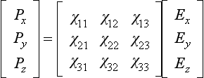
which is simplified for uniaxial crystals by the relationship
Dielectrics which have an inherently asymmetric crystalline structure may be piezoelectric in nature whereby electrical polarisation is produced in response to a mechanical stress, and vice versa. (The effect is to be distinguished from electrostriction, whereby the mechanical strain direction is independent of field polarity.) Some piezoelectric materials are pyroelectric (spontaneously polarised in the absence of an E field and dependent upon heating), whilst some pyroelectric materials are ferroelectric (spontaneously polarised in the absence of an E field and polarisation switched in direction by E). The behaviour of piezoelectric materials is governed by
where s is the mechanical strain, T is the stress, M is Young’s modulus and q the piezoelectric modulus. Such materials have important implications for electromechanical transduction which, in addition to their electronic applications, have power-orientated uses for spark ignition and vibration generation.
The electrical resistance of dielectrics is extremely high so that their insulating properties are enhanced. The equivalent resistance is composed of three components which are the bulk dielectric resistivity, the surface resistivity and an effective resistivity representing the imaginary part of the complex permittivity. The currents which flow in dielectrics are two-fold (equations (4.3) and (4.4))—the conduction current, jc, being less than the displacement current, jd. The insulating nature of dielectrics may be destroyed if the voltage across the dielectric exceeds a critical value. Such failure may occur via three processes: (1) thermal breakdown occurs when the Joule heating of the dielectric exceeds the thermal conduction; (2) dielectric breakdown occurs due to avalanche ionisation in the dielectric; and (3) gas breakdown occurs via voids in solid dielectrics producing chemical degradation of the dielectric. Since the breakdown voltage of the latter is less than that of the dielectric, gas occlusion into solid dielectrics leads to significant degradation of the electrical insulation properties.
4.7 Optical materials
The basic interaction which produces the optical properties of materials is that between the electromagnetic field of light and the electrical charges within the material.
Propagation of light through a transparent dielectric is governed by the refractive index η which is related to the relative permittivity according to
The signal frequency dependence of εr (equation (4.34)) produces dispersion which leads to signal distortion.
For transparent dielectrics which are anisotropic, the refractive index depends upon the plane of polarisation of the light and the material is birefringent. The implication is that the propagation velocity thus depends on the plane of polarisation of the light.
Birefringence may be induced in certain dielectrics through the application of either an external electric field (electro-optics) or mechanical stress (photoelasticity). Electro-optical effects occur due to the E field dependence of the susceptibility
Since 1 ![]() a
a ![]() b, high electric fields (e.g. high-power lasers) comparable to interatomic cohesive forces are needed for the effects to be observable. The quadratic dependence of the polarisation upon the E field corresponds to the Kerr effect and leads to the science of non-linear optics. Situations where the quadratic term is negligible correspond to the Pockel effect. Both effects may be utilised for power system voltage monitoring using optical fibre sensing systems.
b, high electric fields (e.g. high-power lasers) comparable to interatomic cohesive forces are needed for the effects to be observable. The quadratic dependence of the polarisation upon the E field corresponds to the Kerr effect and leads to the science of non-linear optics. Situations where the quadratic term is negligible correspond to the Pockel effect. Both effects may be utilised for power system voltage monitoring using optical fibre sensing systems.
Photoelastic effects arise through the dependence of the polarisation on mechanical stress which follows from the piezoelectric equations (equation (4.41)).
Some transparent materials also exhibit the Faraday effect, whereby the plane of polarisation of the optical signal is rotated through an angle θ in proportion to an applied magnetic flux B according to
where V is the Verdet constant, l the path length, λ the optical wavelength, and η1 and η2 are the refractive indices.
Unlike the electro-optical effects, the magneto-optical effect leads to the rotation of the plane of polarisation being independent of the propagation direction. (The Faraday effect is also observable in certain ferrites at microwave frequencies.)
Reflection of light from the surface of a material occurs due to the incident light polarising charges near to the surface and a re-radiating of light from the oscillating dipole. The reflection coefficient for light at normal incidence depends on the refractive index according to
Light absorption occurs due to ionic polarisation (infrared wavelengths), electronic polarisation (visible—ultraviolet range) and excitation of conducting electrons. Ionic and electronic polarisation give rise to narrow-band absorption, whilst excitation of conducting electrons provides a sharp edged absorption band extending below a critical wavelength.
Light scattering occurs due to atomic-sized particles (Rayleigh scattering, αλ−4) and micrometre sized irregularities (Mie scattering).
Light emission (luminescence) occurs via. fluorescence (emission within 10 ns of energy absorption) or phosphorescence (emission delayed in some cases up to hours).
Energy to produce luminescence may be supplied by higher energy photons (photoluminescence), electron beams (cathodoluminescence), oscillating electric fields (electroluminescence), or by heating following activation by the above (thermoluminescence).
4.8 The plasma state
The plasma state may be formally defined as an ionised material in which the concentrations of ions and electrons are approximately equal and are relatively high. Examples of such plasmas are high-temperature gases such as those occurring in electrical discharges (e.g. electric arcs and high-power gas lasers), the ionosphere, or in certain semiconductors.
The electromagnetic behaviour of such materials is governed by the plasma frequency (ωp) which is the natural frequency of the collective motion of the charges forming the plasma
where N is the number density of the electrical charges. The significance of this parameter is that it governs the refractive index of the plasma according to
where ω is the angular frequency of the electromagnetic wave. Thus the interaction of electromagnetic waves with a plasma depends upon the wave frequency. For ω < ωp, n is imaginary which implies that such waves are reflected. Thus waves of different radiofrequencies are reflected by different ionospheric layers; metals and semiconductors transmit at short electro-magnetic wavelengths and reflect longer wavelengths. The electromagnetic behaviour of such plasmas is, therefore, more complicated than that of conventional conductors, dielectrics or magnetic materials.