Digital Control Systems
Transistor transistor logic (TTL) 14.2.5
Complementary metal oxide semiconductor (CMOS) logic 14.2.6
Emitter coupled logic (ECL) 14.2.7
Conversion between P of S and S of P representations 14.3.5
Formal minimisation, the Quine-McCluskey method 14.3.6
Counters and shift registers 14.7
Sequencing and event driven logic 14.8
14.1 Introduction
14.1.1 Analog and digital circuits
Signals in process control are conventionally transmitted as a pneumatic pressure or electrically as a voltage or current. These signals are said to be continuously variable in that they can take any value between the two extreme limits. Such systems are called analog systems.
Digital circuits are concerned with signals that can only take certain values. Most digital circuits deal with electrical signals that can only have two values; 5 V or 0 V for example. Many circuits are inherently of this type, a light can be on or off, a valve open or shut, a motor running or stopped.
14.1.2 Types of digital circuits
Digital applications can, in general, be classified into three types. The simplest of these are called combinational logic (or static logic), and can be represented by Figure 14.1. Such systems have several digital inputs and one or more digital outputs. The output states are uniquely defined for every combination of input states, and the same input combination always gives the same output states.

Figure 14.1 Representation of a combinational logic system. The output states are defined only by the input state
A sequencing logic system is superficially similar to Figure 14.1 but the output states depend not only on the inputs but also on what the system was doing last (i.e. its previous state). Sequencing systems therefore have memory and storage elements. A very simple example is the motor starter of Figure 14.2(a). The start input causes the motor to start running and keep running even when the start signal is removed. The stop input stops the motor. The action is summarised on Figure 14.2(b). Note that with neither signal present the motor could be running or stopped dependent on which signal occurred last; i.e. the output state is not defined solely by the present input states.
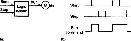
Figure 14.2 A simple sequencing system: (a) representation of a start/stop motor starter; (b) operation, the output depends not only on the input state, but also on the last operation
The final group of digital systems uses digital signals to represent, and manipulate, numbers. Such systems cover the range from simple counters and digital displays to complex arithmetic and computing circuits.
14.1.3 Logic gates
The simplest digital device is the electromagnetic relay, and it is useful to describe some of the fundamental ideas in terms of relay contacts. In Figure 14.3(a), the coil Z will energise when contact A and contact B and contact C are made. The series connection of contacts performs on AND function.
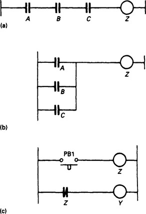
Figure 14.3 Simple relay logic: (a) AND combination, relay Z is energised when A & B & C are all energised; (b) OR combination, relay Z is energised if A or B or C is energised; (c) Inversion, relay Y is energised when PB1 is not made
Similarly, in Figure 14.3(b) the coil Z will energise when contact A or contact B or contact C are made. The parallel connection of contacts performs an OR function.
In Figure 14.3(c), coil Z is energised when the push button is pressed. A normally closed contact of Z controls coil Y. When Z is energised, Y is de-energised and vice versa. The normally closed contact can be said to invert the state of its coil.
Combinational logic circuits are built round combinations of AND, OR and INVERT circuit. In Figure 14.4(a), for example, Z will be energised for:

Figure 14.4 More complex relay logic: (a) Z is energised when (A is not energised) AND (B is energised OR C is energised); (b) Stairwell lighting circuit. A and B are the switches at the top and bottom of the stairs. Changing either switch will change the state of relay Z
(A not energised) AND (B energised OR C energised)
Such verbal descriptions are impossibly verbose for more simplex combinations. Circuit operations are more conveniently expressed as an equation. Normally closed contacts are represented by a bar over the top of the contact name (e.g. A, verbalised as A bar). The circuit of Figure 14.4(a) can then be represented as:
Similarly the circuit of Figure 14.4(b) (commonly used for stairwell lighting) can be represented by:
These are known as Boolean equations, a topic discussed further in Section 14.3.3.
Relays can perform all logic functions but are slow (typically 10 to 20 operations per second), bulky and power hungry. Electronic circuits performing similar functions are called logic gates. These work with signals that can only have two states. A signal in CMOS logic, for example, can be at 12 V or 0 V and could represent a limit switch made or open. The two logic states can be called high/low, on/off, true/false and so on. The usual convention, however, is to call the higher voltage ‘1’ and the lower voltage ‘0’. For a CMOS gate, therefore, 12 V is 1 and 0 V is 0.
Figure 14.5(a) shows the circuit of a simple AND gate. Neglecting diode drops, the output Z will be equal to the lower of the two input voltages. In other words, it will be a 1 if, and only if, both inputs are 1. This can be represented by Figure 14.5(b) (which is called a truth table). On circuit diagrams it is clearer to use logic symbols rather than the actual circuit diagram. The symbol for an AND gate is shown on Figure 14.5(c); the output Z being 1 when A AND B are both 1.

Figure 14.5 A simple diode based AND Gate: (a) circuit; (b) truth table; (c) logic symbol; (d) BS logic symbol
On Figure 14.6(a) the output Z will be equal to the higher of the two inputs (again neglecting diode drops). Z will therefore be 1 if either input is 1 giving the truth table of Figure 14.6(b). The logic symbol for an OR gate is shown on Figure 14.6(c).
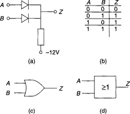
Figure 14.6 A simple diode based OR gate: (a) circuit; (b) truth table; (c) logic symbol; (d) BS logic symbol
The invert function is given by the simple saturating transistor of Figure 14.7(a). When A is 0, the transistor is turned off and the output Z is pulled to a 1 state by the collector load resistor. When A is 1, the transistor is saturated on taking Z to 0 V; a 0. The circuit behaves as the truth table of Figure 14.7(b) and has the logic symbol of Figure 14.7(c).

Figure 14.7 A transistor inverter: (a) circuit; (b) truth table; (c) logic symbol; (d) BS logic symbol
Combinational logic circuits can be drawn purely in terms of AND gates, OR gates and inverters. The stairwell lighting circuit of Figure 14.4(b) is drawn with logic symbols on Figure 14.8(a). This behaves as the truth table of Figure 14.8(b) which shows that Z is 1 if only one input is 1. This circuit is known as an Exclusive OR and is sufficiently common to merit its own logic symbol shown on Figure 14.8(c).

Figure 14.8 An Exclusive OR (XOR) gate: (a) circuit; (b) truth table; (c) logic symbol; (d) BS logic symbol
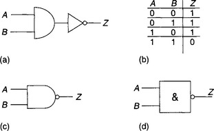
If an inverter is used after an AND gate as Figure 14.9(a), the truth table of Figure 14.9(b) is produced. This arrangement is called a NAND gate (for NOT-AND) and has the logic symbol of Figure 14.9(c). The NAND gate is probably the commonest logic gate.
Adding an inverter to an OR gate as Figure 14.10(a) gives the truth table of Figure 14.10(b). This is known as a NOR gate (for NOT-OR) and is given the logic symbol of Figure 14.10(c).
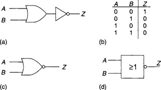
Note that the logic symbols for NAND/NOR gates are similar to those of the AND/OR gates with the addition of a small circle on the output. The circle denotes an inversion operation.
14.2 Logic families
Most logic circuits are constructed from integrated circuits, and have high operating speed and well defined levels. Two logic families (TTL and CMOS) are widely used in industrial applications and a third family (ECL) may be encountered where very high speed is required. Before these are described, we must first examine how the various factors of a logic gates performance are specified.
14.2.2 Speed
A logic gate does not respond instantly to a change at its input. For infinitely fast input signals the output will be delayed and the edges slowed as shown on Figure 14.11. The delay is called the propagation delay and is defined from the mid point of the input signal to the mid point of the output signal. Typical values are around 5 nS for TTL.
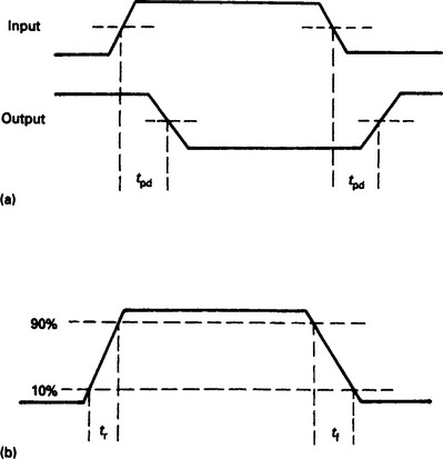
The edge speeds are defined by the rise time (for the 0 to 1 edge) and the fall time (for the 1 to 0 edge). These are measured between the 10% and 90% points of the output signal. Typical values are 2 nS for TTL.
Propagation delays and rise/fall times determine the maximum speed at which a logic family can operate. TTL can operate in excess of 10 MHz, basic CMOS around 5 MHz and ECL at over 500 MHz (although considerable care needs to be taken with board layout at speeds over 10 MHz).
Power consumption is related to speed, as increased speed is obtained by reducing RC time constants formed by stray capacitance, and by using non saturating transistors. CMOS, for example, has a power consumption of about 0.01 mW per gate compared with ECL’s figure of 60 mW/gate.
14.2.3 Fan in/fan out
The output of a logic gate can only drive a certain load and remain within specification for speed and voltage levels. There is therefore a maximum number of gate inputs a given gate output can drive. A simple gate input is called a standard load, and is said to have a fan in of one. A gate output’s drive capability is called its fan out, and is defined in unit loads. A TTL gate output, for example, can drive ten standard gate inputs and correspondingly has a fan out of ten.
Some inputs appear as a greater load than a standard gate. These are defined as a fan in of an equivalent number of standard gate inputs. An input with a fan in of three, for example, looks like three gate inputs. Obviously the sum of all the fan in loads connected to a gate output must not exceed the gate’s fan out.
14.2.4 Noise immunity
Electrical interference may cause 1 signals to appear as 0 signals and vice versa. The ability of a gate to reject noise is called its noise immunity. Defining noise immunity is more complex than it might at first appear, but the method usually adopted is that shown on Figure 14.12(a). The voltages given are those for a TTL gate which has a nominal 1 V of 4.5 V and a nominal 0 V of 0 V.

Figure 14.12 Definitions of noise immunity: (a) D.c. noise margin. The voltages shown are for standard TTL; (b) A.c. noise immunity. The test sees what is the smallest pulse amplitude that will propagate through the chain
Next we define how far an output 1 can fall to (2.4 V) and a 0 rise to (0.4 V). These are respectively termed VOH and VOL. Finally we define how low a gate’s input 1 can fall and an input 0 rise without allowing its output to go between VOH and VOL. These voltages are called VIH (2.0 V) and VIL(0.8V). The noise immunity is then the smaller of (VOH − VIH) or (VIL − VOL). For TTL the figure is 0.4 V. This is a worse case value, a more typical noise immunity is about 1.2 V.
A figure sometimes quoted is the AC noise margin. This is defined as the largest pulse that will not propagate down a chain of gates similar to Figure 14.12(b). This gives a more favourable result than Figure 14.12(a), but is a more realistic test.
14.2.5 Transistor transistor logic (TTL)
TTL is NAND based logic, with the circuit of a 2 input NAND gate being shown on Figure 14.13. The rather odd looking dual emitter transistor can be considered as two transistors in parallel or three diodes as shown.

Figure 14.13 Transistor transistor logic (TTL) circuit diagram the multi-emitter transistor can be considered to act as two transistors in parallel or three diodes
If both inputs are high, Q2 is turned on by current from R1 supplying base current to Q3. The output is therefore nominally 0 V. With either input low, Q1 is turned on, Q2 turned off and Q4 pulls the output high to a nominal 4.5 V.
The output transistors Q3, Q4 are called a totem pole output and play a significant part in increasing the operating speed. When the output is a 0, Q3 acts as a saturated transistor. When the output is a 1, Q4 acts as an emitter follower. Both states have low output impedances which reduce RC time constants from stray capacitance.
There are at least six versions of TTL with differing speeds and power consumption. Schottky versions (with S as part of the suffix) use Schottky diodes within the gate to reduce hole storage delays. All TTL are members of the so called 74 series (originally conceived by Texas Instruments) and have the same pin arrangements on the ICs. They can also be intermixed although care must be taken because of the different input loadings and output capability (an LS gate input, for example, looks like half a normal gate input). All run on a 5 V supply and use nominal logic levels of 4.5 V and 0 V.
14.2.6 Complementary metal oxide semiconductor (CMOS) logic
CMOS is virtually the ideal logic family. It can operate on a wide range of power supplies (from 3 to 15 V), uses little power (approximately 0.01 mW at low speeds), has high noise immunity (about 4 V on a 12 V supply) and very large fan out (typically in excess of 50). It is not as fast as TTL or ECL but its maximum operating speed of 5 MHz is adequate for most industrial purposes. (Too high a maximum speed can actually be a disadvantage as it makes a system more noise prone.)
CMOS is built around the two types of field effect transistors shown on Figure 14.14. From a logic point of view these can be considered as a voltage operated switch. These switches can be used to manufacture logic gates.

Figure 14.15(a) shows how an inverter can be implemented. With A low, Q1 is turned on and Q2 off. With A high Q2 is turned on and Z is low.

Figure 14.15 Complementary metal oxide semiconductor (CMOS) logic gates: (a) NAND gate; (b) NOR gate
Similarly a NAND gate can be constructed as Figure 14.15(b). If A or B is low, Z will be high because one of the parallel pair Q1, Q2 will be on, and one of the series pair Q3, Q4 will be off. The output Z will be low only when both A and B are high when Q1, Q2 are both off and Q3, Q4 are both on.
Figure 14.15(c) shows a CMOS NOR gate. If A or B is high, one of Q3 or Q4 will be on taking the output Z low (with one of Q1, Q2 off). When both A and B are low, Q1, Q2 will both be on and Q3, Q4 off taking the output high.
The high input impedance of FETs can present handling problems, and early devices could be irreparably damaged by static electricity from, say, nylon clothing or leakage currents from unearthed soldering irons. Modern CMOS now includes protection diodes and can be treated like any other component.
Another effect of the high input impedance is the tendency for unused inputs to charge to an unpredictable voltage. All CMOS inputs must go somewhere; even unused inputs on unused gates on multigate packages must go to a supply rail thereby forcing a 1 or 0 state.
CMOS is generally sold in the so called 4000 series which is a rationalisation of the original RCA COSMOS and Motorola McMOS ranges. ‘B’ suffix CMOS denotes buffered signals and improved protection; needless to say the B devices are better suited for industrial systems.
14.2.7 Emitter coupled logic (ECL)
ECL is the fastest commercially available logic family, and with care it can operate at 500 MHz. At these speeds, however, extreme care needs to be taken with the circuit board layout to avoid crosstalk and power supply induced noise. ECL obtains its speed from the use of non saturating transistors and high power levels (around 60 mW per gate compared with CMOS figure of 0.01 mW). The logic levels in ECL are −0.8 V and −1.6V (giving a rather poor noise immunity of 0.25 V). ECL is very fast, but its odd voltage levels, strict wiring and power supply requirements and poor noise immunity preclude its use in industrial applications except where very high speed is needed.
14.2.8 Open collector and tri-state outputs
The TTL NAND gate of Figure 14.16(a) has a single output transistor rather than the usual totem pole output. The output is connected to Vcc by an external pull up resistor. This is known as an open collector output. In Figure 14.16(b) the outputs of several open collector gates are connected in parallel with a single pull-up resistor. A half circle on the gate output symbol is often, but by no means universally, used to show an open collector output. The output Z will be high if, and only if, all the parallel gates have high outputs. Using positive logic conventions the paralleled outputs provide a positive AND function on the outputs of the input gates.

Figure 14.16 An open collector TTL NAND gate: (a) circuit diagram; (b) logic function using open collector gates. The linking of the collectors gives a positive AND or negative OR function depending on the interpretation of the logic states
Another description of the operation is the output Z will be low if any of the outputs are low. This will occur if (A and B are high) OR (C and D are high) OR (E and F) are high. The linking of collectors can be considered to perform a negative OR function on the outputs of the input gates and can give a possibly complex function for the cost of a single pull up resistor. Its main disadvantage is a poor rising edge (caused by the RC time constant of the pull up resistor and stray capacitance) and a slight degradation of noise immunity.
Open collector gates are a possible solution for applications where many devices communicate via a bus system, the backplane of a computer is a typical application. A more common approach for bus systems though is the tri-state gate. Strictly speaking tri-state is a registered trade mark of National Semiconductors. The term tri-state is a bit of a misnomer as the gate does not have three logic levels but rather three logic states: high, low and disconnected. A tri-state gate has normal inputs plus a separate control input which enables the gate or puts the output into a high impedance (disconnected) state. Figure 14.17(a) shows the symbol for a tri-state two input NAND gate and Figure 14.17(b) shows three tri-state buffers which are used to route data from A, B or C to output Z as selected by control inputs L, M or N. It should be noted that this is fundamentally different from the wire AND open collector circuit of Figure 14.16.

14.2.9 Schmitt triggers
Many logic elements require fast edges to operate correctly. Edges can be degraded for a variety of reasons; stray capacitance or a non digital device for example. The Schmitt trigger always gives fast edges on its output signals regardless of the edge speed of the input signals.
The transfer function of a conventional gate is shown on Figure 14.18(a). The transfer function of a Schmitt trigger incorporates hysteresis and is shown on Figure 14.18(b). Figure 14.18(d) shows a slow changing input and the resulting output, which always has fast clean edges.

Figure 14.18 The Schmitt trigger: (a) operation of a conventional inverter; (b) operation of an inverter with hysteresis; (c) logic symbol; (d) use of a Schmitt trigger to convert a slowly changing signal to a crisp digital signal
A Schmitt trigger has the conventional logic symbol with an added hysteresis loop similar to Figure 14.18(c). Schmitt triggers are usually available in hex inverter or quad two input gate ICs. The 74123, for example, is a popular quad two input Schmitt trigger NAND gate.
Comparison of Figures 14.18(a) and 14.18(b) shows that a Schmitt trigger has better noise immunity than a conventional gate. They are therefore commonly used for interfacing to slow and possibly noisy signals from the outside world.
14.2.10 Choosing a logic family
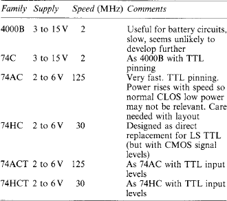
Until the latter part of the 1980s the designer really had to choose between TTL (with the low powered Shottky (LS) family being the popular choice) and CMOS. The latter was slower and had a much smaller range of devices, but had the advantages of very low power consumption, better noise immunity and a wide supply tolerance. Since then, though, there has been a tendency for the families to merge.
The trend started with the 74C series of CMOS which provided CMOS devices with the same pinning as TTL, but with CMOS B series electrical characteristics (slower than TTL, but with 3 to 15V supply). These were useful, but the major impact was the introduction of the 74HC, 74AC, 74HCT and 74HCT families. These use improved technologies, were as fast as TTL, and (as their name implies) they follow the 74 series pinning. Taking them in turn:
74AC is the high speed member of the family, capable of operating at speeds of 125 MHz. The voltage supply range is 3 to 6 V (essentially TTL with a wider tolerance), and the transfer characteristic is the standard CMOS near ideal symmetrical curve of Figure 14.19(a).

74HC is a near replacement for LS TTL with an operating speed of 30 MHz. Other characteristics are similar to 74AC.
As mentioned earlier, the output levels of TTL, shown on Figure 14.19(b), are approximately 0.5 V in the 0 state, and 4.5 V in the 1 state. Standard forms of TTL can, just, connect to 74AC or 74HC devices, but the resultant noise immunity is poor. Two further forms of CMOS were developed with a transfer function whose input side mimicked a TTL device. These are known as 74ACT (high speed version) and 74HCT (practically a direct replacement for LS TTL). These should NOT be viewed as a family to be used for a complete project, as to do so would give the poorer TTL noise immunity. They are, though, exceedingly useful when a circuit has to mix TTL and CMOS devices.
In CMOS, therefore, there is now:
An interesting development is the view that the corner supply pins on TTL are not the best arrangement for power supply and ground noise, and there seems to be a move toward centre pinning on some high speed CMOS circuits.
There are four TTL families in common current use; LS, ALS, F and AS. It is worth listing these in tabular form:
| Family | Speed (MHz) |
| 74LS | 25 |
| 74ALS | 35 |
| 74F | 100 |
| 74AS | 105 |
All require a 5V+/-0.25V supply. The suffix in the above table appears as part of the device identification; a 74LS06, for example, is a low power Schottky gate.
Choosing a device is quite straightforward. First where there is little choice; for out and out speed use ECL (but remember the precautions needed to avoid noise). For high speed, use 74AC (but again take care with the layout).
Battery circuits are best designed with 4000B or 74C devices, the supply is less critical, and both will run on a 9 V battery until it is flat without the need of a regulator circuit. Being slower they are also less prone to noise.
For ‘cooking’ logic, 74HC seems best suited with a reasonable speed, lower power and better noise immunity than LS TTL. The only problem is an incomplete coverage of the TTL family at present (the useful 7490/92 counters are missing for example), so the odd LS or ALS TTL circuit may be needed, with 74HCT devices being used as interfaces between TTL and CMOS.
Figure 14.20 shows a comparison between these families.

14.3 Combinational logic
Combinational logic is based around the block diagram of Figure 14.21(a). Such systems have several inputs and one, or more, outputs. The output states are uniquely defined for each and every combination of inputs and the ‘block’ does not contain any device such as storage, timers or counters. We therefore have n inputs I1 to In and Z outputs Q1 to Qz. In systems with multiple outputs it is usually easier to consider each separately as Figure 14.21(b), allowing us to consider the circuit as Z blocks, each different but represented by Figure 14.21(c).

Figure 14.21 Combinational logic block diagrams: (a) the generalised problem with n inputs and Z outputs; (b) problem split into Z independent circuits; (c) one of the Z circuits with a single output
The number of possible input states depends on the number of inputs:
For two inputs there are four input combinations
and so on. Not all of these may be needed. There are frequently only a certain number of input combinations that may occur because of physical restrictions elsewhere in the system.
The design of combinational logic systems first involves examining all the input states that can occur and defining the output states that must occur for each and every input state. A logic design to achieve this is then constructed from the gates described in Section 14.1.3. In many systems the design can be done in an intuitive manner, but the rest of this section describes more formal design procedures.
Few real life systems need pure combinational logic, most need storage and similar dynamic functions. Such systems can be analysed and designed considering them as smaller subsystems linked together. The design of dynamic systems is discussed in Section 14.8.
14.3.2 Truth tables
A truth table is a useful way of representing a combinational logic circuit, and can be used to design the circuit needed to achieve a desired function.
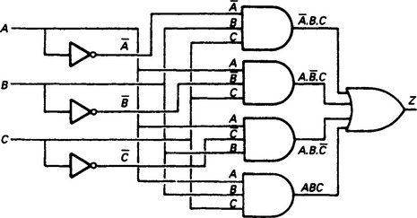
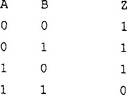
Suppose we have three contacts monitoring some event (overpressure in a chemical reactor for example) and we wish to construct a majority vote circuit. If the three switches are called A, B, C and the majority vote Z this would have the truth table:

It can be seen that Z is 1 for:

The desired logic function can then be constructed directly from the truth table as Figure 14.22. In general, the circuit derives from a truth table will consist as a set of AND gates whose outputs are OR’d together. This form of circuit is known as a Sum of Products (see Section 14.4.3), and one of the reasons for the popularity of NAND gates is that an s of p expression can be formed purely with NAND gates.
A truth table design always gives a design which works and is logically correct, but does not always give a circuit which uses the minimum combination of gates. To do this we need one of the other techniques described below.
This has the simple circuit of Figure 14.23(a), which obviously fulfils the logic function. Consider, however, the totally NAND based circuit of Figure 14.23(b). Straightforward, if laborious, testing of all possible sixteen input states will show that it behaves identically to Figure 14.23(a). In some mysterious way, the right-hand NAND gate is behaving as an OR gate.
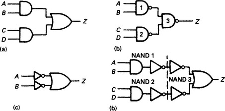
Figure 14.23 Sum of products (AND/OR) logic implementation based solely on NAND gates: (a) required function; (b) NAND based circuit; (c) representation of a NAND gate; (d) circuit b redrawn in the style of representation c. The inverters cancel giving the required function
This rather surprising fact is a result of De Morgan’s theorem, described in the next section. Intuitively, however, we can see the reason by drawing up the truth table for the OR gate preceded by inverters as Figure 14.23(c):
This is the same as a NAND gate, so a NAND gate can, with legitimacy, be drawn as Figure 14.23(c).
The circuit of Figure 14.23(b) could now be drawn as Figure 14.23(d) with the ingoing NANDs drawn as ANDs followed by an inverter, and the outgoing NAND by the arrangement of Figure 14.23(c). Obviously the intermediate inverters cancel, leaving the equivalent circuit of Figure 14.23(a).
14.3.3 Boolean algebra
In the nineteenth century a Cambridge mathematician and clergyman George Boole, devised an algebra to express and manipulate logical expressions. His algebra can be used to represent, design and minimise combinational logic circuits.
The AND function is represented by a dot (.), so
means Z is 1 when A is 1 AND B is 1. Often the dot is omitted (e.g. Z = AB)
The OR function is represented by an addition sign (+), so
means Z is 1 when A is 1 OR B is 1.
The invert function is represented by a bar -, so
means Z takes the opposite state to A. Some sources use the ’ to denote inversion so ![]() and A′ both mean the inverse of A.
and A′ both mean the inverse of A.
Boolean algebra allows complex expressions to be written in a concise manner and can also be used to simplify expressions. To achieve this, a series of rules are used. The first eleven of these are self obvious (or can be visualised by considering the equivalent relay circuits).
(e) A.A = A (e and f are known as the Idempotent laws)
(g) ![]() (known as the Involution law)
(known as the Involution law)
(h) ![]() (h and i are known as the Complementary laws)
(h and i are known as the Complementary laws)
(j) A + B = B+ A (j and k are known as the Commutative laws)
The next two laws, called the Associative laws, allow us to group brackets around variables with the same operator
(l) (A + B) + C = A + (B + C) = A + B + C
(m) (A.B). C = A.(B.C) = A.B.C
The next two laws are called the Absorption laws, and tell us what happens if the same variable appears with AND and OR operators
The next laws, called the Distributive laws, tell us how to factorise Boolean equations
In general, Boolean expressions can be expressed in two forms. The first form, called product of sums, or P of S, brackets OR terms and ANDs the results for example:
The second form, called sum of products, or S of P, groups AND terms and ORs the results, for example:
Truth tables, described in Section 14.4.2, inherently give an S of P result.
The complementary function of a Boolean expression yields the inverse of the expression (i.e. where the expression yields 1, the complement yields 0). The expressions (A + B) and (![]() ) for example, can be shown to be complementary by simply constructing their truth tables.
) for example, can be shown to be complementary by simply constructing their truth tables.
The last two laws, known as De Morgan’s theorem, show how to form the complement of a given expression (and gives one way to interchange S of P and P of S forms).
In its formal representation, De Morgan’s theorem appears rather daunting. It can be more easily expressed:
To form the complement of an expression
For example, to complement the expression ![]()
Step 1, replace ‘+’ by ‘.’ and ‘.’ by ‘+’ giving:
Boolean Algebra can be used to minimise logical expressions, but the method is rarely obvious, and it is easy to make errors with double bars and swapping of ‘.’ s and ‘+’ s. Minimisation by Boolean algebra makes good examination questions, but is rarely used in practice. An easier way to achieve minimisation is to use the graphical Karnaugh map, described below.
14.3.4 Karnaugh maps
A Karnaugh map is an alternative way of presenting a truth table. The map is drawn in two dimensions; two, three and four variable maps are shown on Figure 14.24.

Each square within the map represents one line on the truth table. For example:
square X represents A = 1, B = 0 which can be written ![]()
square Y represents A = 0, B = 1, C = 1 which can be written ![]()
square Z represents A = 1, B = 0, C = 1, D = 0 which can be written ![]()
The essential feature of a Karnaugh map is the way in which the axes are labelled. It will be seen that only one variable changes for a move between any adjacent horizontal or vertical squares
The use of this feature is not immediately apparent, but consider Figure 14.25. This contains four terms giving a 1 output. These are:

so we could write (quite correctly)
Examination of the map, however, shows that the D variable and B variable can change state without affecting the output. The circled squares, in fact, represent AC, so the above expression can be simplified to
Groups of two adjacent cells on a three variable map represent some combination of TWO of the three variables. On Figure 14.26(a), groupings for A.B and ![]() are shown. This map represents
are shown. This map represents

Figure 14.26 Grouping of two adjacent cells: (a) on a three variable map; (b) on a four variable map
Two adjacent cells on a four variable map represent some combination of three of the four variables. On Figure 14.26(b), groupings for ![]() and
and ![]() are shown. This map thus represents
are shown. This map thus represents
Groups of four adjacent cells on a three variable map represent a single variable. The group on Figure 14.27(a) represents the variable A, hence

Figure 14.27 Grouping of four adjacent cells: (a) on a three variable map; (b) on a four variable map
Groups of four adjacent cells on a four variable map represent some combination of two of the four variables. The groups on Figure 14.27(b) represent ![]() and BD. The map represents
and BD. The map represents
A group of eight adjacent cells on a four variable map represent a single variable. The group on Figure 14.28 represents C and ![]() , so
, so

It is important to realise that top and bottom edges are considered adjacent as are right and left sides. Grouping can therefore be made around the tops and sides as Figure 14.29 which represents

The rules for minimisation using Karnaugh maps are simple and straightforward:
(1) Plot the Boolean expression or truth table onto the Karnaugh map
(2) Form new groups of 1s on the map. Groups must be rectangular and contain 1, 2, 4 or 8 cells. Groups should be as large as possible and there should be as few groups as possible. Do not forget overlaps and possible round the edge groupings.
(3) From the map, read off the expression for each group. The minimal expression is then obtained in S of P form, and can be directly implemented in AND/OR gates or NAND gates
Figure 14.30(a) shows a majority vote circuit (2 out of 3) plotted onto a Karnaugh map and grouped as Figure 14.30(b). It will be seen that this has three terms giving the simple NAND based circuit of Figure 14.30(c).

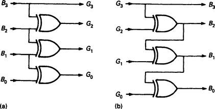
14.3.5 Conversion between P of S and S of P representations
It is occasionally required to translate an S of P expression into a P of S expression and vice versa
These are most conveniently handled in the form
where Nn is the numerical equivalent of the binary pattern at the corresponding gate input. If, for example, a gate input is ![]() , will be 6 corresponding to 110.
, will be 6 corresponding to 110.
The first step is to note the largest number, which determines how many bits we are dealing with (three bits for seven or less, four bits for fifteen or less and so on.) Call the maximum number corresponding to this number of bits Nmax (seven, fifteen, thirty-one etc.).
Note the unused numbers in the expression to be converted. For each unused number Nun there will be a number (Nmax − Nun) in the expression in the other form. For example, to convert the S of P expression
to P of S form we first note Nmax is seven (three bits). The terms in the P of S representation will be given by
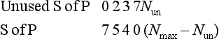
Giving a P of S representation of
Z = Λ (0, 4, 5, 7) which is the equivalent to the original S of P expression.
14.3.6 Formal minimisation, the Quine-McCluskey method
The Karnaugh map is an excellent way of minimising combinational logic, but is essentially limited to five inputs and relies on human intuition. More formal methods are needed for more complex functions. The most common of these is Quine-McCluskey. The method can deal with any number of inputs, but is lengthy and error prone for direct human implementation. It is, however, ideally suited for computer implementation.
The start point is an S of P expression in the form
From this the minterms are grouped according to whether they have one, two, three etc. 1s in them. For example, with


Each term in each group is compared with each term in the group immediately below. If one and only one digit difference is found, a new entry in the lower group is formed with X replacing the single differing digit. Comparing 0010 with 0011 gives a new entry of 001X in the lower table. For the above groups this gives:

The letters a, b, c etc. show the comparisons made and the groups created. Any group which does not create a new group is called a prime implicant, denoted by # above. These are X011, 10X1, 1X01, 0X1X, 01XX, X10X (representing DCBA, A being the least significant as usual) with X denoting don’t care. X011 is thus ![]() . An S of P circuit based on these prime implicants will work, but is not necessarily minimal.
. An S of P circuit based on these prime implicants will work, but is not necessarily minimal.
Next a chart is drawn of these prime implicants, as shown on Figure 14.31 where each prime implicant is represented by a ![]() . For four bit numbers, each minterm with full four bits will have one
. For four bit numbers, each minterm with full four bits will have one ![]() , with one X there will be two
, with one X there will be two ![]() s and with two crosses four
s and with two crosses four ![]() s. X011, for example, represents minterms 3 and 11. The first stage is to identify columns with only a single
s. X011, for example, represents minterms 3 and 11. The first stage is to identify columns with only a single ![]() . The corresponding prime implicants MUST be in the final expression. These are noted down and all the corresponding
. The corresponding prime implicants MUST be in the final expression. These are noted down and all the corresponding ![]() s marked for each row as these are now covered.
s marked for each row as these are now covered.

Figure 14.31 Prime implicant chart after essential implicants and subsequent minterms have been marked
For each column, if there is a marked ![]() in the column, all
in the column, all ![]() s in the column can now be marked, as this minterm has been included. If a prime implicant has all its
s in the column can now be marked, as this minterm has been included. If a prime implicant has all its ![]() s marked it is redundant and can be deleted (e.g. 01XX).
s marked it is redundant and can be deleted (e.g. 01XX).
There will probably be one or more ![]() s left unmarked. Choose from the remaining prime implicants to give the best grouping. Give preference to minterms with the largest number of Xs, and remember that once a single
s left unmarked. Choose from the remaining prime implicants to give the best grouping. Give preference to minterms with the largest number of Xs, and remember that once a single ![]() is marked in a column, all the
is marked in a column, all the ![]() s in the column can be marked. When all
s in the column can be marked. When all ![]() s have been marked a solution has been reached.
s have been marked a solution has been reached.
Following this procedure for Figure 14.31 gives:
a result which could, in all honesty, have been arrived at much faster with a Karnaugh map and common sense. The procedure is, however the basis of computer minimisation of logic circuits as used in PLA and PAL configuration programs.
14.3.7 Hazards, races and glitches
Gate propagation delays discussed in Section 14.2.2 can cause unwanted random pulses to appear in logic circuits. These unwanted pulses are known variously as hazards, races or glitches.
The logical output of Figure 14.32(a) should always be zero since
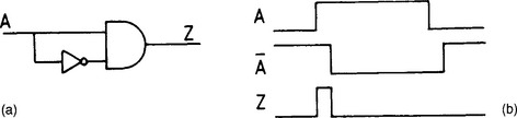
Figure 14.32 An obvious glitch producing circuit: (a) logic diagram, the output should always be ‘0’; (b) actual circuit behaviour
In practice, however, ![]() will be delayed by the propagation delay of an inverter giving the possible waveforms of Figure 14.32(b). As A changes a small pulse may appear at the output.
will be delayed by the propagation delay of an inverter giving the possible waveforms of Figure 14.32(b). As A changes a small pulse may appear at the output.
Glitches are not always immediately obvious. A similar problem can occur with the NAND based AND/OR circuit of Figure 14.33(a). This implements the relationship
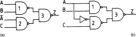
Figure 14.33 Non obvious glitch producing circuit: (a) logic diagram; (b) redrawn to show source of the glitch
As before ![]() must be obtained from some form of inverter as Figure 14.33(b). The circuit is logically correct but if B = C = 1 then the circuit is behaving in a similar way to Figure 14.32(a). If B and C are both 1 and A changes state a small pulse will probably appear at the output.
must be obtained from some form of inverter as Figure 14.33(b). The circuit is logically correct but if B = C = 1 then the circuit is behaving in a similar way to Figure 14.32(a). If B and C are both 1 and A changes state a small pulse will probably appear at the output.
Plotting Figure 14.33 onto a Karnaugh map as Figure 14.34(a) shows a way to identify and eliminate glitches. There are two groups on the map; AB and ![]() . Moving between AB = 11 and AB = 01 we move between groups. This corresponds to A changing from 1 to 0 or 0 to 1. A potential glitch has adjacent 1s not covered by the same group.
. Moving between AB = 11 and AB = 01 we move between groups. This corresponds to A changing from 1 to 0 or 0 to 1. A potential glitch has adjacent 1s not covered by the same group.
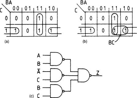
Figure 14.34 Glitch free design using a Karnaugh map: (a) original minimal grouping; (b) BC term added to remove the glitch. The final grouping is non minimal; (c) the resulting glitch free, but non minimal, logic
To remove the risk of a glitch we add an additional group as Figure 14.34(b). There are now no adjacent 1s not in the same group. The resulting circuit is shown on Figure 14.34(c). Note that the group BC is logically redundant and is included solely to prevent glitches when A changes state with B = C = 1. Glitch free circuits are often non minimal.
Glitches may not always be important. In general, if the output of a glitch prone circuit is not feeding directly (or indirectly) a counter, storage device or timer the glitches will probably have no effect. Glitches can also be ignored by using clocked synchronous systems. Different logic families have different propensities for generating and ignoring) glitches. The important factor is the relationship between edge speeds and propagation delays. CMOS, with edge speed similar to or longer than the propagation delay, has a useful tendency to ignore glitches. ECL, with very fast edge speeds, is very prone to glitches.
14.3.8 Integrated circuits
Many complex functions are available in IC form, and a circuit designer should aim to minimise cost and the number of IC packages rather than the number of gates. A minimisation exercise, whether by Boolean algebra or Karnaugh map, should always be preceded by a search of an IC catalogue for a suitable off the peg device.
14.3.9 UCLAs, PALs and PLAs
An integrated circuit consists of a small slice of silicon into which is etched the various individual unconnected components required to make the required circuit. These are then connected by a thin metallised layer to form the required device function. An UCLA (for uncommitted logic array, also known as an ULA) consists initially of a large number of assorted gates, storage and memories but without the metallised interconnection layer. The user specifies the required circuit which is then formed by the design of the metallised layer. The basic IC silicon slice (which is the expensive part) is thus common to many users and the relatively cheap metallisation layer is specific to one user’s application. UCLAs therefore allow designers to have their own ICs at a reasonable price. They are, though, only cost effective for reasonable volume production runs.
An alternative approach, suitable for smaller volumes, is programmable logic. These are essentially a combination of true/complement inputs with an AND/OR output as shown on Figure 14.35. Each connection point is originally linked, but can be blown open by the designer (using a programming terminal) to leave the desired function. The original devices were based on bipolar construction, and literally used small metallic fuses. Once blown, they could not be re-used. Later MOS devices can be erased by UV light in a similar way to EEPROMs.

The simplest devices use a programmable AND combination (selected from the true/complement inputs) with a fixed AND/OR logic. These are known as Programmable Array Logic, or PALs. The more versatile (but more complex) arrangement of Figure 14.36 uses programmable AND plus programmable OR connections. These are known as Programmable Logic Arrays or PLAs, (this distinction is not quite true, the terms PLA and PAL are used interchangeably by some manufacturers).

Figures 14.35 and 14.36 are essentially combinational logic in sum of product (S of P) form (see Section 14.3.2). Sequential programmable logic is also available, and is typically of the form of the Figure 14.37 based around an AND/OR/D-type circuit. These are known as registered or sequential PALs. They are very useful for building logic networks built around state transition diagrams (see Section 14.8)

Figure 14.37 Sequential programmable logic with tri-state outputs. A typical device would have eight inputs and eight D type flip flops
There are some disadvantages. Early devices had a voracious power appetite, several hundred mA for some. The later MOS devices are better, but their use should be questioned on battery driven devices. There is also a one-off investment needed in a programming terminal, and programming languages such as ABEL, CUPL and PALASM. These work out the required link blowing from a designer specified logic function defined in combinational or state transition form. They do not, however, check out for glitches and even seem to encourage them by aiming for truly minimal logic. Some care is needed by the designer, but the languages do allow redundant combinations to be specified to give glitch free circuits.
With bipolar devices, it should also be remembered that bipolar devices cannot be reprogrammed if an error is made. Mistakes with bipolar programmable logic are not cheap, and even with MOS versions, erasure with UV light is not instantaneous.
Programmable logic is very popular where standard boards (with fixed connections to the outside world) can be used in different applications. Typical examples are vending and ticket machines, interface devices or testing of a logic circuit before building the final version.
14.4 Storage
Most logic systems require some form of memory. A typical relay circuit is the motor starter circuit of Figure 14.38 which ‘remembers’ which of the two operator push buttons was pressed last. The memory is achieved by the latching contact A1.

14.4.2 Cross coupled flip flops
The logical equivalent of Figure 14.38 is the cross coupled NOR gate circuit of Figure 14.39(a). Assume both inputs are 0, and output Q is at a 1 state. The output of gate a will be 0, and the two 0 inputs to gate b will maintain Q in its 1 state. The circuit is therefore stable. If the reset input is now taken to a 1, Q will go to a 0. and ![]() to a 1. Similar analysis to that above will show that the circuit is stable in this state, even when the reset input goes back to a 0.
to a 1. Similar analysis to that above will show that the circuit is stable in this state, even when the reset input goes back to a 0.

Figure 14.39 A NOR based RS flip flop. This circuit remembers which input was last a ‘1’: (a) logic diagram; (b) operation; (c) logic symbol
The set input can be used now to switch the Q output to 1 and the ![]() back to a 0. The set and reset inputs cause the output to change state, with the outputs indicating which input was last at a 1 state as summarised by Figure 14.39(b). If both inputs are 1 together, both outputs go to a 0, but this condition is normally disallowed.
back to a 0. The set and reset inputs cause the output to change state, with the outputs indicating which input was last at a 1 state as summarised by Figure 14.39(b). If both inputs are 1 together, both outputs go to a 0, but this condition is normally disallowed.
The cross coupled NOR gate circuit is called an RS Flip Flop, and is shown on logic diagrams by the symbol of Figure 14.39(c).
It is also possible to construct a cross coupled flip flop from NAND gates as Figure 14.40(a). Analysis will show that this behaves similar to Figure 14.39, but the circuit remembers which input last went to a 0 as shown on Figure 14.40(b). The logic symbol for a NAND based RS flip flop is shown on Figure 14.40(c); the small circles on the input showing that the flip flop responds to 0 inputs.

14.4.3 D type flip flop
The D type flip flop shown on Figure 14.41(a) has a single data input (D), a clock input and the usual Q and ![]() outputs. Superficially this is similar to the latch memory above, but the clock operates in a more subtle way. The operation of a typical D type flip flop is shown on Figure 14.41(b). The clock samples the D input when the clock input goes from a 0 to 1, but the output changes state when clock goes from 1 to 0. The significance of this is explained below in Section 14.4.6.
outputs. Superficially this is similar to the latch memory above, but the clock operates in a more subtle way. The operation of a typical D type flip flop is shown on Figure 14.41(b). The clock samples the D input when the clock input goes from a 0 to 1, but the output changes state when clock goes from 1 to 0. The significance of this is explained below in Section 14.4.6.

Figure 14.41 The D type flip flop: (a) logic symbol; (b) operation; (c) logic diagram for a master/slave D type
There are several ways in which a D type flip flop can be implemented. A common circuit uses the master/slave arrangement of Figure 14.41(c). When the clock input is I. the D input sets, or resets, the master flip flop. When the clock input is 0 the state of the master flip flop is transferred to the slave flip flop (and the outputs take up the state of D when the clock input was 1). Note that the master flip flop is isolated from the D input whilst the clock is 0.
Although it would be feasible to construct a master/slave flip flop from discrete gates, integrated circuit D types (such as the TTL 7474 or the CMOS 4013) are readily available.
14.4.4 The JK flip flop
In Section 14.4.2 the NOR based RS flip flop was described, and it was stated that the input state R = S = 1 was normally disallowed. The JK flip flop, shown on Figure 14.42(a) is a clocked RS flip flop with additional logic to cover this previously disallowed state. The clock input acts as described above for the D type flip flop, i.e. sampling the inputs on one edge, and causing the outputs to change on the other.
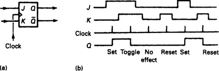
The outputs after a clock pulse for J = 1, K = 0; J = 0, K = 1; J = 0, K = 0 are as would be expected for a clocked RS flip flop. If J = K = 1, the outputs toggle; that is the states of the Q and ![]() interchange. This action is summarised on Figure 14.42(b).
interchange. This action is summarised on Figure 14.42(b).
The toggle state is the basis for counters, described in Section 14.7.
14.4.5 Clocked storage
The D type and JK flip flops described above are examples of clocked storage. The advantages, and implications of this are probably not immediately obvious.
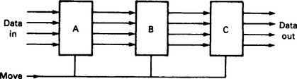
In all bar the simplest systems, data is often required to be moved around from one storage position to another. In Figure 14.43, for example, data is to be moved through stores A, B, C in an orderly manner. If simple flip flops were used along with a signal enable as shown, the data would shoot straight through all the stages. If clocked storage is used, the data will sequence from A to B to C, moving one position for each clock pulse.
14.5 Timers and monostables
Control systems often need some form of timer. Timing functions in logic circuits are provided by devices called monostables or delays. There are many types of delay, although all can be considered as Figure 14.44(a), to consist of an input, Q and ![]() outputs and an RC network which determines the delay period.
outputs and an RC network which determines the delay period.
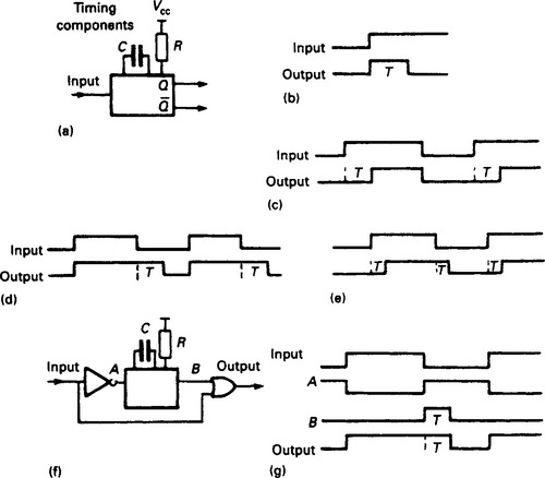
Figure 14.44 Various forms of timers and monostables: (a) basic form of a timer. The timer duration is determined by the values of R and C and is usually of the order of RC seconds; (b) one shot timer, often called a monostable; (c) delay on timer; (d) delay off timer; (e) delay on and off timer; (f) delay off timer built using a simple monostable; (g) timing waveforms for circuit f
The commonest timer, often called the one shot or monostable, gives an output pulse, of known duration, for an input edge. The user can select which edge (0→1 or 1→0) triggers the circuit. On Figure 14.44(b) a 0→1 edge is used. Monostables are the basis of all other delay circuits and are widely available (74121, 74122 in TTL, 4047, 4098 in CMOS). Pure delays are shown on Figure 14.44(c–e), and these can be constructed by adding gates to monostable outputs. Figure 14.44(f/g) shows the circuit for a delay off.
A variation of the monostable is the retriggerable monostable. In most monostables circuits the timing logic ignores further input edges once started. In a retriggerable monostable each edge sets the timing circuit back to the start again. The action of a retriggerable and normal monostable are compared on Figure 14.45.

The time delay of any timer is of the order of RC seconds where R is the value of the timing resistor in ohms and C is the value of the timing capacitor in farads. For delays of more than a few seconds very large values of R and C are required. High value resistors are prone to changes in value from leakage and large value capacitors must be electrolytics with problems from leakage, size and long term drift. For periods of more than a few seconds it is usually better to produce a time delay with an oscillator and counter as Figure 14.46. The oscillator produces a free running pulse chain which is normally blocked by gate 2. A start pulse sets flip flop 3 and resets the counter. With flip flop 3 set, pulses are passed to the counter which counts up. When the counter reaches a pre-determined count it resets the flip flop. The Q output of the flip flop thus goes high for a time

where N is the count preset and P the oscillator period. Integrated circuits based on this principle, such as the ZN1034, are available giving very long delays (up to days) with reasonable value components and little problems from drift.
14.6 Arithmetic circuits
14.6.1 Number systems, bases and binary
In previous sections, logic signals have been assumed to represent events such as printer ready, or low oil level. Digital signals can also be used to represent, and manipulate numbers.
We are so used to the decimal number system that it is hard to envisage any other way of counting. Normal every day arithmetic is based on multiples of ten. For example, the number 9156 means:

Each position in a decimal number represents a power of ten. Our day to day calculations are done to a base of ten because we have ten fingers. Counting can be done to any base, but of special interest are bases 8 (called octal), 16 (called hex for hexadecimal) and two (called binary).
Octal uses only the digits 0–7, the octal number 317, for example, means
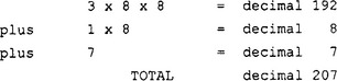
Hex uses the letters A—F to represent decimal ten to fifteen, so hex C52, for example, means
Binary needs only two symbols, 0 and 1. Each position in a binary number represents a power of two and is called a bit, for Binary digiT, most significant to the left as usual, so 101101 is evaluated:

Fractions can also be represented in binary, although this is not commonly encountered. Taking fractions as powers of two we get 1/2 (0.1 in binary), 1/4 (0.01 in binary), 1/8 (0.01) and so on. The binary number 110.101 is thus 6 plus 0.5 plus 0.125 giving 6.625.
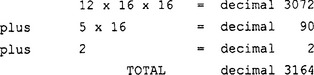
Conversion from decimal to binary is achieved by successive division by two noting the remainders. Reading the remainders from the top (LSB) to bottom (MSB) gives the binary equivalent. For example, decimal 23
Octal and hex give a simple way of representing binary numbers. To convert a binary number to octal, the binary number is written in groups of three (from the LSB) and the octal equivalent written underneath, for example 11010110
Hex conversion is similar, but groupings of four are used. Taking again the binary number 11010110;
The octal number 326 and the hex number D6 are both representations of the binary number 11010110.
14.6.2 Binary arithmetic
This is evaluated in three stages:

At each stage we consider three ‘inputs’; two digits and a possible carry from the previous stage. Each stage has two outputs, a sum digit and a possible carry to the next, more significant state. A single digit adder can therefore be considered as Figure 14.47(a). Several single digit adders can be cascaded, as Figure 14.47(b), to give an adder of any required number of digits. Note the carry out of the most significant stage becomes the most significant digit.

Figure 14.47 Adder circuits: (a) representation of a one digit adder. This block diagram will be the same regardless of the number base used; (b) construction of a four digit adder from four identical one digit adders; (c) one bit (i.e. one digit) binary adder logic diagram
Binary addition is similar, except that there are only two possible values for each digit. If Figure 14.47(a) is a binary adder, there are eight possible input combinations:

An example of binary arithmetic is
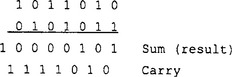
The implementation of the adder truth table is a simple problem of combinational logic; one possible solution is shown on Figure 14.47(c). In practice, of course, adders such as the TTL 7483 are readily available in IC form.
Negative numbers are generally represented in a form called two’s complement. The most significant digit represents the sign, being 1 for negative numbers and 0 for positive numbers. The value part of the number is complemented and 1 added. For example:
+ 12 in two’s complement is 01100 (the MSB 0 indicating a positive number).
To get to two’s complement for −12 we complement 1100 giving 0011, set the MSB to 1 giving 10011 then add 1 giving 10100 which is the two’s complement representation of −12.

In each case, addition of the positive and negative number will give the result zero, e.g.

The top carry is lost, giving the correct result of zero.
Two’s complement representation allows subtraction to be done by adding a negative number, for example 12-3

The top bit is lost giving the correct result of +9.
Multiplication and division are rarely required in simple logic systems and are generally best implemented with some form of microprocessor assembly in conjunction with specialist mathematical co-processors such as the AMD9511. If a hardware solution is required it can be based on the addition of weighted partial sums. Consider the decimal multiplication

The multiplicand is multiplied by each digit of the multiplier in turn and the part results added with appropriate weighting to give the result. Binary multiplication is similar but simpler in that only four multiplication results need to be considered:
A typical binary multiplication is therefore

Note that multiplying two four bit numbers can give an eight bit result. If two binary numbers A & B are to be multiplied, therefore, partial sums are obtained by multiplying (i.e. gating) A by each bit of B to form as many partial sums as there are bits in B. These partial sums are then weighted and added to give the result as above.
The fastest multiplication can be obtained by using Read Only Memories (ROMs) programmed with an entire multiplication table. The multiplicand and the multiplier then act as the ROM address and the result is simply read. Two 1 k bit ROMs can form a four by four multiplier with no additional logic. The 74284 & 74285 are integrated circuits designed specifically for this purpose.
Division is even rarer, but can also be performed using ROMs.
14.6.3 Binary coded decimal (BCD)
A single decimal digit can take any value between 0 and 9. Four binary digits are therefore needed to represent one decimal digit. In BCD, each decimal digit is represented by four bits. For example:
BCD is not as efficient as pure binary. 12 bits in pure binary can represent 0–4095, compared with 0–999 in BCD. BCD, however, has advantages where decimal numbers are to be read from decade switches or sent to digital displays.
14.6.4 Unit distance codes
Figure 14.48 shows a possible application of binary coding. The position of a shaft is to be measured to 1 part in 16 by means of an optical grating moving in front of four photocells. The photocell outputs give a binary representation of the shaft angular position.

Consider what may happen as the shaft goes from position 7 (0111) to position 8 (1000). It is unlikely that all the cells will switch together, so we could get
![]()
or any other lengthy sequence of four bits. These possible incorrect intermediate states can be avoided by using a code in which only one bit changes between adjacent positions. Such codes are called unit distance codes.
The commonest unit distance code is the Gray code, shown in four bit form below.
It will be noted that the code is reflected about the centre. Sometimes the term ‘reflected code’ is used for unit distance codes. A unit distance code can be constructed to any even base by taking an equal number of combinations above and below the centre point of a Gray code. A decimal version (called the XS3 cyclic BCD code) is also shown. In this code zero is 0010, one is 0110, two is 0111 and so on to nine which is 1010.
Conversion between binary and Gray code is straightforward, and is achieved with XOR gates as shown on Figure 14.49(a) and (b).

14.7 Counters and shift registers
Counters are used for two basic purposes. The first, and obvious, use is the counting, or totalising, of external events. The second use of counters is the division of a frequency to give a new, lower frequency.
The ‘building block’ of all counters is the toggle flip flop which changes state each time its clock input is pulsed. Usually the. toggling occurs on the negative edge as shown on Figure 14.50(a). A toggle flip flop can be constructed from JK or D type flip flops as shown on Figure 14.50(b, c).

Figure 14.50 The toggle flip flop: (a) operation, the output changes state for each input pulse; (b) a JK toggle flip flop; (c) a D type connected to make a toggle flip flop
If the Q output of a toggle flip flop is connected to the clock input of the next stage as shown on Figure 14.51(a), a simple binary counter can be constructed to any desired length. Figure 14.51 is a 3 bit counter with A the LSB and C the MSB. This counts:

Another pulse will take it to state 0 again. It can be seen that Figure 14.51 is counting up. To count down, the Q outputs are connected to the input of the following stage and the signal outputs taken from the Q lines.
There are two limitations to the speed at which a counter chain similar to Figure 14.51 can operate. The first is the maximum speed at which the first (fastest) stage can toggle. The second restriction is not so obvious.
Consider the case of an 8 bit counter going from 01111111 to 10000000. The LSB toggling causes the next to toggle and so on to the MSB. The change has to propagate through all 8 bits of the counter, so circuits similar to Figure. 14.51 are called ripple counters. During the ‘ripple’ the counter will assume invalid states and cannot be sensibly read. Obviously the propagation delay through all the stages should be considerably less than the input period. High speed applications use synchronous counters, described below.
In Figure 14.51 the frequency of output C is precisely one eighth of the input frequency. A simple ripple counter can therefore also act as a frequency divider. If we define
then N = 2m for m binary stages.
It will also be seen that the output of any stage of a binary counter has equal mark space ratio regardless of the input mark/space providing the input frequency is constant.
Although it is feasible to construct ripple counters with D type and JK flip flops it is usually more cost effective to use MSI ICs such as the TTL 7493 4 bit counter or the CMOS 4024 7 bit counter. These incorporate features such as a reset line to take the counter to a zero state.
14.7.2 Synchronous counters
Ripple counters are limited in both speed and length by the cumulative ripple through propagation delay and also temporarily exhibit invalid outputs. Although these limitations are not important in slow speed applications, they can cause difficulties in high speed counting.
These restrictions can be overcome by the use of a synchronous counter where all required outputs change simultaneously. There is no ripple propagation delay through the counters and no transient false count stages. The only speed restriction is the toggling frequency of the first stage.
The building block of a synchronous counter is the JK flip flop/AND gate arrangement of Figure 14.52(a). If the T input is 1, the JK flip flop will toggle on the receipt of a clock pulse. If the T input is D, the flip flop will not respond to a clock pulse. The carry output is 1 if T is 1 and Q is 1.

Figure 14.52 Synchronous counters: (a) basic circuit for a synchronous counter; (b) four bit series connected synchronous up counter
A synchronous up counter is constructed as Figure 14.52(b), which is simply the circuit of Figure 14.52(a) repeated. Note that the clock input is common to all stages, and the carry from one stage is the T input of the next.
It will be seen that the T inputs, Tb, Tc, Td will be 1 when all the preceding outputs are 1. Tc will be 1, for example, when A and B are both 1. This is the condition when a counter stage should toggle, taking DCBA from, say, 0011 to 0100.
It is also possible to construct a synchronous down counter by counting the AND gate input of Figure 14.52(a) to the Q output rather than the Q, and observing the counter state on the Q output. A synchronous up/down counter with selectable direction can be constructed as Figure 14.53. If the direction line is a 1, gates 1, 2, 3 are enabled, the Q outputs pass to the next stage and the counter counts up. If the direction line is a 0, gates 4, 5, 6 are enabled, the Q outputs pass to the next stage and the counter counts down.

14.7.3 Non binary counters
Counting to non binary bases is often required, a BCD count is probably the most common requirement. When the required count is a subset of a straight binary count, (e.g. BCD), the circuit of Figure 14.54(a) can be used. The counter output is decoded by external logic. When the counter reaches the desired maximum count the decoder output forces the counter to its zero state (which is 0000 for a BCD counter, but need not be for other counters).

Figure 14.54 Non binary counters: (a) principle of operation; (b) logic diagram for a BCD up counter; (c) counter operation
A single BCD stage constructed on these principles is shown on Figure 14.54(b). The circuit shown is a ripple counter, but could equally well be a synchronous counter. Gate A detects a count of ten (binary 1010) and resets the counter to zero via direct reset inputs on the JK flip flops. Waveforms are shown on Figure 14.54(c).
Where a non binary count is needed (e.g. a Gray code count), it is best to use synchronous counters and an arrangement similar to Figure 14.55. This is drawn for D type flip flops, but JK based design is similar.
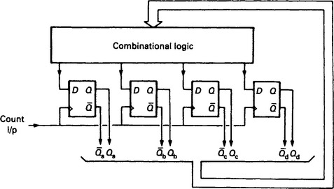
Figure 14.55 Generalised synchronous non binary counter using D type flip flops. Any count pattern can be produced with this arrangement. The principle can also be implemented using JK flips flops.
A combinational logic network looks at the counter outputs and sets the D inputs for the next state. If the counter, say, was required to step from 1101 to 0011, the combinational logic output to the D inputs would be 0011 for an input of 1101. Effectively there are four combinational circuits in the network, one for each D input.
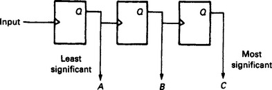
14.7.4 Shift registers
A simple shift register is shown on Figure 14.56(a). Data applied to the serial input, S in, will move one place to the right on each clock pulse as shown on the timing diagram of Figure 14.56(b).

Figure 14.56 Simple shift register constructed from D type flip flops: (a) logic diagram; (b) operation
Shift registers are used for parallel/serial and serial/parallel conversions. They are also the basis of multiplication and division circuits as a shift of one place towards the MSB is equivalent to a multiplication by 2, and one place towards the LSB an integer division of 2.
14.8 Sequencing and event driven logic
Many logic systems are driven by randomly occurring external events, and follow a sequence of operations. In such systems, the output states do not depend solely on the input states, but also on what the system was doing last. These types of systems are said to be sequencing and event driven logic. Sequencing logic is designed using a state diagram. This shows the possible conditions the system can be in, the conditions that are required to move from one state to the next, and the outputs required in each state.
Figure 14.57 shows a possible state diagram for a gas burner control. When the start PB is pressed a 15 second air purge is given (set by timer 1). The pilot valve is opened, and the igniter started for 4 seconds (timer 2). If, at the end of this time, the flame detector shows the flame to be lit, the main gas valve is opened. At any time the stop button terminates the sequence. A non valid signal from the flame detector (i.e. flame present in states 1 and 2 or no flame in state 4) puts the system to an alarm state, as does the incorrect signal from the air flow switch. Note that these are checked for being ‘unfrigged’ at the start of the sequence.

Event driven logic is built around flip flops, usually one for each state. The flip flop corresponding to state 4 is shown on Figure 14.58(a), and is set by the required conditions from state 3 and reset by the possible next states (1 and 5). Outputs are simply obtained by ORing the necessary states. The pilot output, shown on Figure 14.58(b), is simply State 3 OR State 4.

Figure 14.58 Implementation of a state diagram: (a) one of the five states of the gas burner control. Each state is represented by a flip flop and is set by transitions to the state and reset by transitions from the state; (b) one of the seven outputs. Each is simply an OR function of the states in which it is energised. The pilot valve is energised in states 3 and 4.
It is possible to minimise event driven circuits to use fewer flip flops, but such an approach is usually not required as it makes the operation more difficult to understand. A straightforward state diagram similar to Figure 14.57 is easy to design, understand and modify and simplifies fault finding for maintenance personnel.
State diagrams are being formalised by the International Electrotechnical Commission (IEC) and the British Standards Institute (BSI), and already exist with the French Standard Grafset. These are basically identical to the approach outlined above, but introduce the idea of parallel routes which can be operated at the same time. Figure 14.59(a) is called a divergence; state 0 can lead to state 1 for condition ‘s’ OR to state 2 for condition ‘t’ with transitions ‘s’ and ‘t’ mutually exclusive. This is the form of the state diagrams described so far.

Figure 14.59 State transition diagram symbols: (a) divergence; (b) simultaneous divergence; (c) convergence; (d) simultaneous convergence
Figure 14.59(b) is a simultaneous divergence, where state 0 will lead to state 1 AND state 2 simultaneously for transition V. States 1 and 2 can now run further sequences in parallel.
Figure 14.59(c) again corresponds to the state diagrams described earlier, and is known as a convergence. The sequence can go from state 5 to state 7 if transition ‘v’ is true OR from state 6 to state 7 if transition ‘w’ is true.
Figure 14.59(d) is called a simultaneous convergence (note again the double horizontal line) state 7 will be entered if the left-hand branch is in state 5 AND the right-hand branch is in state 6 AND transition ‘x’ is true.
The state diagram is so powerful that most medium size PLCs include it in their programming language in one form or another. Telemecanique give it the name Grafcet (with a ‘c’), others use the name Sequential Function Chart (SFC) (Allen Bradley) or Function Block (Siemens). The IEC have adopted state diagrams as one of their formalised methods of PLC programming in IEC 1131.
14.9 Analog interfacing
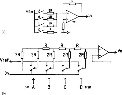
14.9.1 Digital to analog conversion (DAC)
A binary number can represent an analog voltage. An 8 bit number, for example, represents a decimal number from 0 to 255 (or −128 to +127 if two’s complement representation is used). An 8 bit number could therefore represent a voltage from 0 to 2.55 V, say, with a resolution of 10 mV. A device which converted a digital number to an analog voltage is called a digital to analog converter, or DAC.
Common DAC circuits are shown on Figure 14.60, in each case the output voltage is related to the binary pattern on the switches. In practice, FETs are used for the switches, and usually an IC DAC is used. The R-2R ladder circuit is particularly well suited to IC construction.
14.9.2 Analog to digital converters (ADCs)
There are several circuits which convert an analog voltage to its binary equivalent. The two commonest are the ramp ADC and the successive approximation ADC. Both of these compare the output voltage from a DAC with the input voltage.
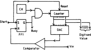
The operation of the ramp ADC, shown on Figure 14.61, commences with a start command which sets FF1 and resets the counter to zero. FF1 gates pulses to which counts up. The counter output is connected to a DAC whose output ramps up as the counter counts up. The DAC output is compared with the input voltage, and when the two are equal FF1 is reset, blocking further pulses and indicating the conversion is complete. The binary number in the counter now represents the input voltage. A variation of the ramp ADC, known as a tracking ADC uses an up/down counter that continuously follows the input voltage.
The ramp ADC is simple and cheap, but relatively slow (typical conversion time > 1 mS). Where high speed, or high accuracy is required a successive approximation ADC is used. The circuit, shown on Figure 14.62 uses an ordered trial and error process. The sequence, shown on Figure 14.63, starts with the register cleared. The MSB is set, and the comparator output examined. If the comparator shows the DAC output is less than, or equal to, Vin, the bit is left set. If the DAC output is greater than Vin, the bit is reset. Each bit is similarly tested, in order from MSB to LSB, causing the DAC output to quickly home in on Vin as shown. In total the number of comparisons is equal to the number of bits, so the conversion is much faster than the ramp ADC.
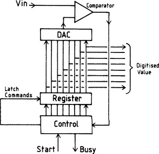

Successive approximation ADCs are fast (conversion times of a few μS) and accurate (0.01% is easily achievable). Unlike the ramp ADC, the conversion time is constant. They are, however, more complex and expensive than the simpler ramp ADC.
The flash converter is the fastest ADC available, but is not widely used for high accuracy applications because the circuit complexity increases rapidly with the number of bits. Commercial eight bit flash encoders such as the MC10135 are to be found in digital television and digital audio applications. Figure 14.64 shows a simple three bit converter with a resolution of one part in eight.

The input signal is compared simultaneously with seven equally spaced voltages, for our simple example these are 1, 2, 3 V etc. If, for example, the input signal is 3.6 V, comparators a, b and c will all give a ‘1’ output, and comparators d to g will give a ‘0’ output.
The outputs from the seven comparators are converted to a three bit binary output by an encoder. This is simple combinational logic, output C, for example, being given by
The complexity of the combinational logic goes up considerably with the number of bits and the degree of internal checking required.
The flash converter is very fast with conversion times of a few nanoseconds, the only constraint being the propagation delays through the comparators and the encoder logic. It is, however, prone to giving invalid transitory states if the input signal is varying, going, say, 011 to 111 to 100 for a input change from three to four volts. For this reason a flash converter is usually preceded by a sample and hold circuit to freeze the analog input circuit whilst the measurement is being made.
14.10 Practical considerations
Real life digital systems have to connect to the outside world, and this can often bring problems when noise and effects such as contact bounce are encountered. Precautions also need to be taken against inadvertent introduction of high voltages into logic systems via inter-cable faults on the plant.
All signals between a logic system and the outside world should use a technique called opto isolation when cable lengths are longer than a few metres. Figure 14.65 shows typical input and output circuits. In both, the signal is electrically isolated by using a coupled LED and photo-transistor. Because the plant side power supply and digital power supply are totally separate, the system will withstand voltages of up to 1 kV without damage to the digital equipment (although such voltages would probably damage the plant side components of course). The absence of ground loops and relatively high current levels (around 20 mA) also gives excellent noise immunity.
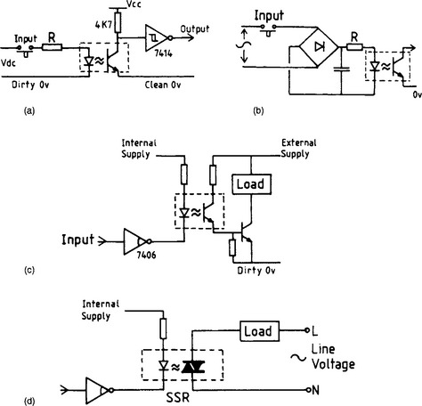
Figure 14.65 Optical isolation between digital system and outside world: (a) d.c. input circuit; (b) a.c. input circuit; (c) d.c. output circuit; (d) a.c. output circuit
Opto isolation devices (such as the TIL 107) are usually constructed in a 6 pin IC, and are characterised by a current transfer ratio. This is defined as the ratio between the photo transistor collector current to the LED current. A typical value is 0.3, so 20 mA input current will give 6 mA, output current. If Darlington phototransistors are used, transfer ratios as high as 1.2 can be obtained.
Noise can also enter digital systems via the power supply rails so excellent filtering is necessary, both the d.c. side and (with LC filter) on the a.c. supply side. It is particularly important to adopt a sensible segregation of 0 V rails such that digital logic, relays/lamps and analog circuits have separate 0 V returns to some common earth points. Under no circumstances should high currents flow along logic 0 V lines, or the logic 0 V be taken outside its own cubicle.
Digital ICs can also generate their own noise on power supplies (TTL is particularly troublesome). It is therefore highly desirable to provide each IC with its own local 0.01 μF capacitor. A single large value electrolytic has no effect as the noise is caused by rapid di/dt and the PCB track inductance.
Mechanical contacts from switches, relays etc, do not make instantly but ‘bounce’ rapidly for 1 to 4 mS due to dirt and the uneven constant surfaces. In many purely combinational logic systems this does not matter, but where counting, sequencing or arithmetic circuits are used, trouble can ensue.
Contact bounce can be removed by RC filters, but the best solution is to use a bounce removing flip flop as Figure 14.66. Provided break before make contacts are used, the circuit gives totally bounce free true and complement outputs. If the contacts are some distance from the digital system opto isolation should, of course, be used before the flip flop.