
Power Semiconductor Devices
The development of power semiconductor devices began in the late 40s and 50s with the bipolar transistor and the power diode, this was followed a decade later by small thyristors and triacs. The thyristor has continued to develop over the years, growing in power and frequency rating, leading to high power press-pack fast switching thyristors and ultra high voltage thyristors in the 70s, and GTO Thyristors in the 80s. In turn these new devices have enabled the development of greater and greater efficiency in a wide range of power conversion systems. However the fundamental disadvantage of these devices was the complexity of the drive and control equipment they require. The first major breakthrough came with the advent of the Power MOSFET in the 70s and 80s. That enabled a major reduction in the complexity of the control systems, and pushed power conversion forward in frequency and efficiency, but the MOSFET would never challenge the thyristor in the high power arena. All this was changed however with the arrival in the 1990s of the high power insulated gate bipolar transistor (IGBT), essentially the single chip integration of a Power MOSFET and a highly efficient bipolar transistor.
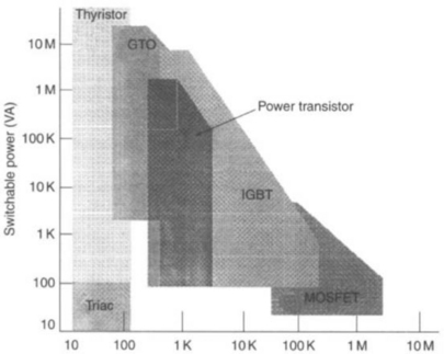
The main types of power semiconductor switching device available today are shown in Figure 17.1 illustrating the spectrum of power and switching frequency occupied by each type, and giving some of their main areas of application. Diodes are not shown on this picture as they encompass the whole range and essentially complement the switching devices. There are still on going developments of all these power switches, some of which will be covered in this chapter, and potentially new materials and new device structures will continue to re-write the story for power semiconductors.
Because of the generally superior performance that can be achieved, almost all power semiconductor devices are made today using monocrystalline silicon, and many of the highest power devices use extremely pure silicon crystals as their starting point. At the top end of the power range single-element silicon devices are available that are able to withstand voltages in excess of 6000 V with average current ratings of 1000 A and voltages of 2000 V with average current ratings of 6000 A. Typically the largest devices (diodes) have a forward volt drop of 1.2 V at 5000 A and a reverse leakage current of less than 100 mA at 5000 V, the voltage that a semiconductor device is able to withstand with a low leakage current is referred to as its ‘blocking voltage’. This demonstrates the very small power loss dissipated in the device compared to the power controlled or rectified and the high efficiency of this type of component. Typically, large power devices of this type are mounted in a package that can be double-side cooled such as that shown in Figure 17.2(d). More recently the plastic power module has become a widely accepted alternative to the double-side cooled press pack, Figure 17.2(b). This module is single-side cooled through an electrically isolated base-plate and has all the power terminals on one face. It has become the preferred outline for the high power IGBT and diode module (see Section 17.6.1). At the other end of the spectrum is the Power MOSFET at a few 10s of watts but able to switch at high speed in the range of 100 MHz.

Power semiconductor devices can be divided into two groups, roughly splitting the power spectrum in two, these are minority carrier devices (bipolar), and majority carrier devices (unipolar). The bipolar device relies on the injection of both minority and majority carriers into a high-resistivity region of the device. This reduces the device on-state voltage by modulating the resistivity of its high-resistivity region and reducing the voltage drop across this region. However, these conductivity-modulated devices such as the diffused p-n junction silicon diode and the thyristor or silicon controlled rectifier (SCR) suffer the disadvantage that the injected carriers or charge must be extracted before a blocking state can be sustained. The charge also cannot be injected or extracted instantaneously into or from the high-resistivity region of the device. This takes some time to occur and during this period, before the low on-state voltage is established or the high blocking voltage can be attained, substantially higher instantaneous power is dissipated in the device. Similarly during turn on, a substantial level of charge must be injected before the device attains its optimum low conductivity state. In the case of a switching device this can result in a high power requirement from the gate drive, and also high instantaneous power during turn on. These phenomena combine to limit the maximum permissible switching speed of these devices. This has also resulted in a number of different types of conductivity-modulated devices being developed. Some of them are specifically optimised for 50 or 60 Hz operation, which are sometimes referred to as ‘converter-grade’ or ‘phase control’ devices. Faster types of devices have also been designed for operation at higher frequencies and are often referred to as ‘inverter-grade’ or ‘fast’ devices. Generally, however, the fastest conductivity modulated devices are limited in practical applications to an operating frequency below 50 kHz.
The second group of devices is the majority-carrier or unipolar device that does not rely on conductivity modulation, for example metal oxide silicon field effect transistors (MOSFETs) and Schottky diodes. In a majority carrier device, current is carried only by the majority carriers. The on-state voltage is therefore dependent on the concentration of majority carriers in the conducting region of the device. Injection of minority charge and conductivity modulation does not occur so that there is no reverse-recovery charge to be extracted on turn-on and turn-off losses are, therefore, much lower, resulting in an optimum operation at higher switching frequencies, as high as 100 MHz in some cases. However, on-state losses will generally be higher since the number of current carriers is restricted although this will also be dependent on the voltage design of the device.
Thus the maximum useful voltage rating of the MOSFET is less than 1000 V, and more typically less than 600 V, however this is quite suitable for most domestic mains voltage equipment, and so unipolar devices are used in very high volumes in such consumer based applications.
A third group of hybrid devices includes most notably the insulated gate bipolar transistors (IGBT) that combine some aspects of conductivity-modulated and majority carrier devices and offers special advantages in many applications. Although more complicated in construction it is the IGBT that has revolutionised power electronics in the more recent years.
It can be seen that in general it is the minority carrier (bipolar) devices which dominate the low frequency high power area, the majority carrier (unipolar) types in the high frequency and low power arena, and the hybrid IGBT which is predominant in the mid range.
17.1 Junction diodes
A p–n junction is made by increasing the concentration of electron or hole populations in certain regions of a monocrystalline silicon disc or chip. This is done by introducing impurity atoms, such as phosphorus with five electrons in its valence band or boron with three electrons in its valence band, to create either electron-rich n-type or hole-rich p-type regions within the crystal lattice, respectively. The conductivity in these regions at normal device operating temperature is wholly determined by the concentration of the impurities introduced.
A depletion region (a region which is devoid of charge carriers and therefore very highly resistive) is established at the point in the crystal where the crystal ceases to become either electron or hole rich and reverts to the opposite type. This is caused by holes diffusing from the p region where they are present in a higher concentration into the n region and alternate electrons diffusing from the n to the p region. This forms an electrical potential barrier at the junction between the p and n regions. Under an externally applied forward bias with the p region held positive to the n region, carriers are injected across this potential barrier and a high current can flow through the diode with only a small voltage appearing across the device. When the p–n junction is biased with p region held negative with respect to the n region the depletion region widens to sustain the voltage and allows only a small reverse current to flow. This is called a reverse biased p–n junction. When the polarity is reversed it is called a forward biased p–n junction and current may flow freely across the junction with only a small resultant voltage drop. A more complete description of the physical behaviour of the p–n junction can be found in reference 1.
17.1.2 The p–n junction power diode
Construction of the power diffused p–n junction diode normally begins with a high-purity defect-free silicon wafer with a very uniform low doping concentration of n-type impurity such as phosphorus. The n-type silicon is preferred as the starting material because it offers a superior reverse-recovery characteristic as explained below. The silicon is then doped by the diffusion of a p-type impurity such as boron, aluminium or gallium at a temperature above 1000°C into one side of the wafer. The p-type diffusion takes place in a diffusion furnace under very carefully controlled conditions. This is followed by a similar high concentration n-type diffusion to the opposite side of the silicon disc to form the impurity concentration profile shown in Figure 17.3. The conductivity and final thickness of the central n-type region together with the final surface area of the silicon device ultimately determines the voltage capability and current rating of the device.

Figure 17.3 (a) Impurity concentration in a p–n junction diffused diode and the injected carrier concentration under forward bias; (b) The electric field distraction across a p–n junction diode under reverse bias
Under high forward bias conditions a high concentration of charge is injected in the central n region resulting in the injected carrier distribution (also shown in Figure 17.3). The injected electron and holes are present in the n region in equal quantities, which maintains charge balance locally throughout the n region. However, as can be seen from Figure 17.3, the concentration of carriers varies across the n region width. The reason for this is that, once injected into the n region, the excess carriers only have a finite lifetime before they recombine with another excess carrier of the opposite charge. Once injected across the p–n junction the injected carrier can on average only travel a certain distance before recombining, which results in the injected charge distribution shown in Figure 17.3. The rate of recombination is governed by the concentration of another type of impurity that provides a recombination centre through which the annihilation occurs. The time taken for the injected carriers to be annihilated is measured by a parameter that is commonly called the minority carrier lifetime. The aim in the construction of converter grade p–n junction diodes is normally to reduce the concentration of these recombination centres to the absolute minimum possible, which typically results in an average carrier lifetime of greater than 100 μs. The conductivity of the n region is therefore increased by the presence of the injected carriers and the on-state voltage of the diode reduced. Thus the greater the minority carrier lifetime, and/or the greater the level of injected charge the lower the on-state voltage.
When the forward current is reduced to zero as the diode recovers its blocking state and reverse bias is applied to the p–n junction diode, it behaves initially like a short circuit until the charge in the central n region is removed. This results in the typical reverse-recovery characteristic shown in Figure 17.4.

The length of time it takes for the diode to recover trr = tA + tB is affected by the carrier lifetime; a long lifetime results in a long recovery time. Also the recovered charge Qrr, which is the charge extracted during the recovery time, increases with increased lifetime. As the reverse voltage is increasing across the diode during this recovery phase, there is an inherent energy loss, or recovery loss, determined by the product of volts and amps, during this phase. Thus there is a trade off between the recovery loss and the on-state voltage (loss) of the diode. This highlights one of the fundamental relationships of all bipolar devices: increasing on-state losses can be traded off against decreasing turn off losses by controlling the minority carrier lifetime, and or the carrier injection levels in the p–n junction.
A p–n junction diode is normally designed so that when the maximum reverse-voltage rating is applied the whole of the depletion region is contained within the central n region of the device. Under these conditions an electric field is established across the depletion region as shown in Figure 17.3. The maximum peak electric field that can be sustained in silicon is between 5 × 10⁴ and 8 × 10⁵V/cm. If the reverse voltage is increased above the maximum reverse voltage rating of the device the reverse-leakage current begins to increase rapidly as the peak electric field exceeds the point where avalanche multiplication of carriers occurs in the depleted region. The voltage at which carrier avalanche multiplication is initiated is called the ‘avalanche voltage’ of the diode. A typical characteristic for a silicon p–n junction diode is shown in Figure 17.5. As the temperature of the p–n junction diode is increased over its permitted operating range its characteristics also change, as illustrated in Figure 17.5. Note that as the junction temperature increases both reverse leakage current and the avalanche voltage increase, whereas the on-state voltage decreases at low current and increases at higher current.

Figure 17.5 Characteristics of a 50 mm silicon p–n junction rectifier. Note the different scales in the different quadrants
The optimum design p–n junction diode with lowest on-state voltage and smallest reverse-recovery charge possible is obtained by manufacturing the device from a silicon crystal with the lowest resistivity and narrowest n-base consistent with the desired voltage rating of the device. As the design target maximum reverse voltage rating of the p–n junction diode is increased the resistivity of the n-type silicon has to be increased to ensure the design voltage is attained before the peak electric field reaches the point where avalanche breakdown occurs across the whole operating temperature range of the device. At the same time the thickness of the n-type region also has to be increased to accommodate the increased depleted region width. Because of the increased n-type-region thickness higher target voltage design p–n junction diodes have a higher on-state voltage at the same forward current and exhibit a larger reverse-recovery charge than lower target voltage design devices of the same surface area. This highlights a second basic relationship for bipolar devices, the device operating losses increase as the voltage rating of the device is increased. A more complete description of the p–n junction design principles is given in reference 1.
17.1.3 Fast-recovery p–n junction power diode
In order to reduce the reverse-recovery charge shown in Figure 17.4 extracted from a fast-recovery p–n junction diode and, thereby, to increase its maximum permissible operating frequency, the diode designer can apply two techniques. These are to reduce the level of charge injected into the diode, or to reduce the minority carrier lifetime in the central n region of the diode.
The lifetime is reduced by increasing the level of recombination centre impurities, as the concentration level of recombination centres is increased, the annihilation rate of the injected carriers increases with the result that the charge extracted during reverse-recovery decreases. However, the reduced reverse-recovery charge has to be traded off against increases in reverse leakage current and on-state voltage. The recombination centres or impurities that are generally used are gold, platinum and radiation damage. Each has its own individual characteristic that determines the shape of the reverse-recovery current after the peak of the reverse-recovery. Therefore, to optimise fully the performance of a fast-recovery p–n junction diode, not only do those parameters described above concerning central n-region resistivity and thickness have to be carefully controlled, but also the concentration and distribution of these recombination centres in the central n region of the device. Lower target voltage design fast-recovery p–n junction diodes constructed from thinner silicon not only have a lower on-state voltage but can also have very much lower reverse-recovery charge than higher target voltage design devices. This is because it is possible to introduce much greater concentrations of recombination centre impurities into lower voltage design fast-recovery diodes before impairing the reverse leakage and on-state voltage characteristics of the diode. However, in practice it is generally necessary to increase the concentration of recombination centre impurities to the point where their introduction has the effect of increasing reverse leakage current significantly. This reduces the maximum permitted operating temperature of fast-recovery p–n junction diodes compared to converter grade diodes, e.g. from 200°C or 175°C down to 150°C or 125°C. For example, a 600 V target voltage design fast-recovery p–n junction diode with an average current rating of 335 A has a maximum reverse-recovery charge of 4 μC. This can be compared to 25 μC for a 1400 V target voltage design fast-recovery p–n junction diode of the same size with an average current rating of 295 A.
One very important feature of fast-recovery diodes used with fast switching components such as IGBTs is called the snappiness of the diode. During initial the recovery phase the charge is extracted by the formation of the depletion region in the n-base, when this charge is extracted very rapidly the device current can fall towards zero too fast, resulting in what is called snap off, and a consequential spike, or a series of oscillations in the recovery voltage waveform. Snappiness is quantified by the ratio between the two time periods of turn-off, tA and tB. A low snappiness factor, combined with a low recovered charge is the ideal situation: this is what is meant by a ‘soft’ fast-recovery diode. This can be a particular problem with p–i–n type diodes described later.
17.1.4 Epitaxial fast-recovery p–n junction power diode
The central n region of a fast-recovery p–n junction diode designed for optimum performance with a target reverse voltage capability of 800 V or less is usually extremely thin and of the order of 70 μm thickness or less. Unfortunately very thin silicon wafers are difficult to handle in manufacturing. One widely used manufacturing technique to manufacture this type of diode is with an epitaxial silicon deposition process. In this process a single-crystal high resistivity n-type silicon layer is grown from a vapour on top of a more highly doped n+ silicon single-crystal substrate. This is followed by a p+ type diffusion process to form the p–n junction of the diode. The substrate is of a low resistance and therefore provides a mechanical support for the active epitaxial diode structure without degrading the diode performance. This technique can be used to manufacture fast-recovery p–n junction diodes that have superior characteristics in certain respects compared to any other fast-recovery p–n junction diode designs. In most other respects the epitaxial fast-recovery p–n junction diode is very similar to the fast-recovery p–n diode. There are, however, a number of constraints imposed by the epitaxial process itself, including cost, which inherently limit the highest resistivity of the n-type layer which can be grown, the thickness of the layer and the degree of perfection to which the crystal can be grown over a large area. In practice, these parameters limit the upper voltage capability of this design to 1600 V with a maximum average current rating of approximately 100 A in a single silicon die.
17.1.5 The p–i–n junction power diode
The p–i–n junction diode is another version of the fast-recovery p–n diode. As explained some of the transient forward and reverse-recovery characteristics of this device can generally be improved by reducing the thickness of the central region of the diode to the absolute minimum. However, the normal fast-recovery p–n junction diode is still designed to contain the whole of the maximum reverse-bias depletion region in its n region (see Figure 17.3). In the p–i–n junction diode the resistivity of the n region is chosen to be almost intrinsic; that is, the concentration of n-type impurities is very low and its resistivity very high. The thickness of that region is also chosen so that the depletion region of the device penetrates to the n+ region when the maximum design reverse voltage is applied as shown in Figure 17.6. It is possible in this way to design fast-recovery p–i–n junction diodes that have an n or i region that is as much as half the thickness of the n region of a conventional fast-recovery p–n junction. The resulting device, therefore, can have a much-reduced reverse-recovery charge because being thinner the base region has a lower effective resistance than that of the p–n diode when flooded with carriers. So it is possible to reduce significantly the base carrier concentration, by limited carrier injection or by lifetime reduction, without such an increase in the on-state voltage drop. For example, a 1400 V target voltage design p–i–n diode with an average current rating of 300 A has a maximum reverse-recovery charge of 8 μC. This compares to 25 μC for a 1400 V diode of the same size and an average current rating of 295 A.

Figure 17.6 Impurity concentration and electric field distribution under reverse bias of a p–i–n junction diffused diode
One disadvantage of the p–i–n junction diode is that its reverse-recovery characteristic exhibits snappy recovery compared to the comparatively soft recovery of the fast-recovery p–n junction diode. This results from the fact that the depletion layer spread during recovery is very rapid in the low doped intrinsic base region. By careful design of the fast diode it is possible to minimise the snappy behaviour of the diode, this is of particular importance for IGBT applications as will be discussed in Section 17.6.
17.2 Bipolar power transistors and Darlingtons
17.2.1 Bipolar n–p–n power transistors
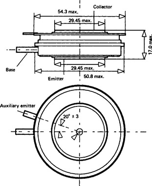
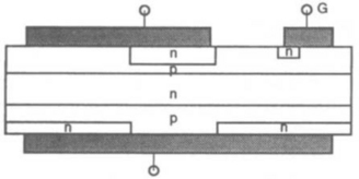
The bipolar power transistor is a three terminal power device that relies on charge modulation to reduce device on-state voltage. Carriers are injected from the emitter region and transit across the base region to be collected at the collector and modulate the resistivity of the lightly doped collector. Almost all high power bipolar transistors produced today are based on the n–p–n type of construction, although the alternative p–n–p type of construction is also produced, mainly for use in complementary switching circuits. However, the same principles of operation apply for both types of device. High power bipolar n–p–n power transistors are available today in the type of package shown in Figure 17.7, made from a single silicon wafer with continuous current ratings of up to 1000 A and peak currents of up to 1200 A and collector emitter sustaining voltages of up to 1000 V. Construction of the device begins with the diffusion of an n-type impurity to form the n+ collector region and this is followed by further p-type and n-type diffusions
This results in the typical bipolar n–p–n power transistor diffusion profile shown in Figure 17.8. An alternative manufacturing procedure replaces the initial n-type diffusion into lightly doped n-type silicon crystal with a high resistivity epitaxial silicon layer grown on a highly doped n-type silicon substrate. The surface structure of the high power bipolar transistor ensures an even distribution of base current over the active area of the device.

Figure 17.8 Diffusion profile of a typical bipolar n–p–n power transistor and on-state injected carrier density
Generally, bipolar n–p–n transistors are operated either in a fully off state or in an on-state and driven between these two states as rapidly as possible to reduce instantaneous power losses. In the off state the base of the device is held at zero or negative bias to minimise collector leakage current. The electric field distribution that typically will exist inside the collector structure when the maximum permitted voltage is applied is shown in Figure 17.9. As can be seen from Figure 17.6, the electric field distribution in the reverse-biased collector region of the bipolar n–p–n power transistor is similar to the reverse bias p–i–n junction power diode. The objective of the two designs is the same, insofar as both aim to achieve as high a reverse blocking voltage capability as possible with the thinnest piece of n-type silicon that can be used.

Figure 17.9 Diffusion profile of a typical bipolar n–p–n transistor and off-slate electric field distribution
Bipolar n–p–n power transistors are usually operated in one of two alternative on-states: saturation or quasi-saturation. However, it is sometimes necessary to operate these devices in the active region shown in Figure 17.10 for certain applications, despite the fact that these devices are not designed and, therefore, not optimised for use in this region. Under these circumstances only a very reduced power-handling capability is possible. In the saturated on-state the collector emitter voltage VCE. is less than that for the forward bias voltage which appears across a simple silicon p–n junction such as a p–n junction diode. This is because the collector base junction becomes forward biased at high collector current and this subtracts from the voltage across the base emitter junction resulting in typical VCE voltages of 0.2–0.3 V. However, in this condition the whole of the base and collector regions of the bipolar n–p–n power transistor are saturated with injected carriers. When a device is switched off under these conditions a considerable amount of charge has to be extracted and this is associated with a long storage time, ts. If the collector voltage is held above 1.5 V the device is said to be in quasi-saturation and the collector base junction is prevented from becoming forward biased.
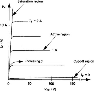
Figure 17.10 Output characteristics of the bipolar junction transistor in the common emitter configuration
To ensure safe switching of a bipolar n–p–n transistor between the off- and on-state a number of basic rules have to be observed. In addition, a large bipolar n–p–n power transistor has a number of important features that can best be understood by reference to Figures 17.11 to 17.16.

Figure 17.11 Transistor switching with a resistive load. (a) IC/VCC trajectories; (b) base current IB and collector voltage VCE (in volts); (c) collector current; (d) instantaneous power loss

Figure 17.12 Transistor switching with an inductive load. (a) IC/VCC trajectories; (b) base current; (c) collector voltage; (d) collector current; (e) instantaneous power losses


Figure 17.15 Transistor switch-on: (a) without a switch-aiding circuit; (b) with a switch-aiding circuit; (c) with a saturable reactor switch-aiding circuit

Figure 17.16 Transistor switch-off: (a) without a switch-aiding circuit; (b) with a snubbing active-capacitor switch-aiding circuit
Figure 17.11 shows the important waveforms involved in resistive load switching of a typical bipolar power transistor. Line A–C in Figure 17.11(a)) shows a voltage-current excursion during both turn-on and turn-off. Turn-on and turn-off switching energy losses can be reduced by minimising the transition time from point A to point C. The delay time (td) and rise time (tri) as defined in Figure 17.11(b)) can be reduced by increasing the turn-on base current (IB1) defined in Figure 17.13 and, thereby, the turn-on losses can be reduced. The fall time (tfi) defined in Figure 17.11(b)) of a saturated transistor can be reduced by optimising dIB2/dt, the rate of application of IB2. Optimisation ensures simultaneous cut-off of the emitter-base and collector-base junctions of the transistor. Once this has occurred the transistor enters the quasi-saturated region. Thereafter, a large value of IB2 may be safely applied and this ensures a minimum fall-time and, thereby, reduces the turn-off losses. A transistor already operating in the quasi-saturation region may have IB2 applied as rapidly as possible, without damage.
Figure 17.12 shows the waveforms involved in switching an inductive load. The switch-on waveform shown in Figure 17.12(a)) is indicated as that part of the switching locus A → B → C and the switch-off waveform C → D → A. The freewheel diode (Df) conducts load current (IL) when the transistor turns off. The diode is assumed to exhibit reverse-recovery characteristics and have an initial load current IM. Consider first the turn-on sequence of the transistor. Assume Df is initially in conduction when VCC is applied across the transistor and stray lead inductance. Df starts to recover but appears initially as a short circuit. When the diode recovers the voltage across the transistor (VCE) falls from VCC to the on-state value and the transistor current increases to full load current value, as shown in Figures 17.12(b), 17.12(c) and 17.12(d). The rate of rise of this current is determined by the magnitude and rate of rise of IB1 and by transistor gain. High-gain transistors driven by large base currents exhibit the lowest turn-on losses. During turn-off the diode will remain non-conducting until VCE reaches the supply voltage VCC. Throughout the rise in VCE all the load current flows through the transistor but, once VCE reaches VCC, IC drops to zero and Df carries on conducting the load current. At this point VCE can exceed VCC by around 10–20V due to the finite turn-on time of Df. The total VCE–IC excursion during inductive switching is as shown in Figure 17.12(a)). By reducing the collector current switching time, energy losses can be reduced and the safe operating area extended. The safe operating area is that portion of VCE−IC switching boundary graph which a load line can traverse without damaging the transistor.
Figure 17.13 shows the relevant base current waveforms. IBI should initially be high during charging of the emitter-base capacitance CBE, that is usually 2–3 times the value required during the full turn-on phase. During free-wheel diode recovery, the transistor will carry the recovery current causing it temporarily to enter the linear region of the VCE–IC characteristic. During the conduction phase, sufficient base current must be applied to keep the transistor fully saturated or quasi-saturated. This current is about 1.5 times that for saturation of a minimum-gain transistor. Application of a negative base current IB2 will remove charge from the base-emitter junction. dIB2/dt must be adjusted so that the emitter-base and collector-base junctions are cut off together. For inductive load switching, as with resistive loads, the quasi-saturated state does not suffer from this limitation.
High-frequency applications tend to favour the quasi-saturated mode of operation. Large IB2 values reduce storage and fall times but, once the ratio IB2/B1 exceeds 3, little further improvement is observed.
In order to improve the voltage hold-off capability and control any dv/dt effects, a reverse bias of at least 3 V needs to be maintained across the emitter-base junction. It is permissible to operate this junction in the avalanche region, provided that power levels are kept low.
Use of a ‘Bakers’ clamp as shown in Figure 17.14 prevents transistor saturation, keeping the transistor in the quasi-saturated regions. Diode Das conducts base current into the collector and prevents the collector voltage from going below a given value. Anti-saturation techniques such as this give shorter storage times and fast turn-off, since there are few excess carriers in the collector that need to recombine with the collector current.
The use of a low-value resistor RBE of approximately 10–100 Ω between the emitter and base terminals increases the transistor blocking capability. Only a small current is diverted through this resistor and power loss is small. The effect of VCE dv/dt can be controlled by applying a negative base-emitter voltage during the off state. Power losses in the RBE resistor then become more significant during the off state than in the transistor on state. As RBE is decreased storage time is also reduced which is due to a lower emitter-base junction capacitance time constant at turn-on.
Switching of transistors, especially with inductive loads, necessarily incurs the simultaneous application of supply voltage VCC and full load current IC as shown in Figures 17.15 and 17.16. Violation of the permitted safe operating area may occur under these conditions which can result in the transistor being driven into secondary breakdown and thermal destruction of the device. Restrictions must therefore be placed on the operating conditions of the transistor.
To avoid simultaneous application of high voltage and high current, the VCE–IC excursion needs to be modified such that its path across the safe operating region does not produce this situation. This also minimises losses and the full rating of the transistor can be obtained. The modification is effected by components that ensure that peak current and peak voltage do not occur together during turn-on and turn-off.
A turn-on aiding circuit is shown in Figure 17.15. The inductance holds off and controls the collector di/dt during turn-on. If the inductor used is non-saturable then di/dt = VCC/L. The inductance L also controls the freewheel diode recovery current.
If the inductance is saturable VCE falls and the inductance initially holds off the supply voltage deficit without much current flow. The inductance then saturates to a low value and supports very little voltage. Losses in the inductance are low since the current required to magnetise it is small. In Figure 17.15(c)) the saturable inductance supports the deficit supply voltage until VCE has fallen to zero. Once the inductor is saturated, the collector circuit non-load inductance becomes very low. The free-wheel diode reverse recovery di/dt is very large, possibly forcing the transistor into the linear region as shown in Figure 17.15(c)) and the addition of a series non-saturable air core inductor may be required.
A resistance Rs in series with the diode speeds up the current decay. Similarly a diode/zener configuration will constrain the inductor voltage and also reduce the current decay time.
A turn-off aiding ‘snubber’ circuit and the waveform excursions developed are shown in Figure 17.16. At turn-off current is diverted from the transistor to the snubber capacitor Cs with the collector voltage clamped to the capacitor voltage. At turn-on Ds blocks and Cs discharges current through Rs and the transistor. The power losses in the resistor are given by Pc = 1/2 Cs VCC2f.
If the collector voltage rise time trv is minimal compared to the IC fall time (tfi), then maximum energy loss during switching in an unaided transistor is given by WT = 1/2IC VCC tfi.
Losses are less for snubber-aided transistors because switching occurs at low VCE voltages, allowing more efficient transistor operation. As CS, is increased, more energy is diverted from the transistor to the capacitor. The energy stored in CS can become very large and must be dissipated as heat in RS during the subsequent turn-on phase. At high voltages and switching frequencies the power rating of RS will become large, making it more desirable to recover the energy in CS.
The ‘snubber’ circuit maintains the transistor load inside the safe region of the curve RBSOA, increasing device efficiency, since most of the energy dissipated in the snubber would otherwise be dissipated by the transistor.
The size of the snubber capacitor determines the snubber effectiveness and its purpose is to yield a desired rate of rise of VCE at a given peak IC. The time interval (+t) of interest for this calculation is that measured from the instant VCE starts to rise at turn-off until IC approaches zero. This time interval also is dependent on reverse-base current applied to the transistor.
RS is chosen to ensure that CS will discharge completely during the conduction time of the transistor.
The power dissipated in a snubber resistor is given by
where f is the frequency of operation. The snubber capacitor increases the fall time of the transistor by slowing the rate of rise of VCE. The crossover point of voltage and current is lowered by the use of a snubber, indicating a reduction in peak power dissipation, as indicated in Figure 17.16. A more complete description of the bipolar n–p–n transistor is given in reference 1 and of the application of the device in reference 2.
17.2.2 Bipolar n–p–n power Darlington transistor
In spite of some disadvantages the monolithic, or one-chip, Darlington transistor continues to be extremely popular for power transistor switching applications. Its main advantage is its high gain with a minimum number of components. The gain of the Darlington is given by the following equation for an unstabilised Darlington
where β1, is the gain of transistor T1 and β2 is the gain of transistor T2 in the simple Darlington configuration shown in Figure 17.17(a)).

The addition of stabilising resistors R1 and R2 as shown in Figure 17.17(b)), which are normally included in the silicon chip, improve storage time but reduce gain. The gain of the Darlington is then given by
when the effect of R1 is neglected.
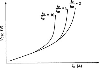
To prevent the Darlington coming out of saturation under overload current conditions, it is necessary to overdrive the base as illustrated in Figures 17.18 and 17.19 and, although the device gain fails, the saturation voltage VCED can be maintained at an acceptable level:
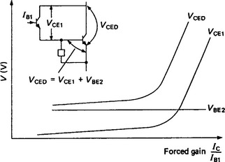
At turnoff however the input transistor T1 displays a storage time tS1 after which IC1 drops resulting in a decrease in IB2. The output from T2 is quasi-saturated with a storage time ts2, and from Figure 17.20 it can be seen that

As IB1 increases with IC held constant, forced gain decreases and tSD increases (Figure 17.21). Since the output transistor is in quasi-saturation, its storage time tS2 is independent of forced gain. Therefore, overdriving the Darlington (Figure 17.17) only influences the storage time of the driver transistor tS1. This can be reduced if a negative base current is withdrawn from T1. However, if the ratio of negative to the positive base current is increased, the effect on tSD diminishes, as shown in Figure 17.22. Any further reduction in tSD can only be brought about by reducing tS2 that can be achieved by fitting a speed-up diode D1, as shown in Figure 17.23. When D1 is fitted the emitter-base junction of T1 is by-passed. A negative base current will then flow into T2 if a negative bias −VBB is applied to R1, which reduces TS2, but only after the emitter-base diode of T1 begins to become reverse biased. Current flowing in D1 then reverse biases the emitter-base junction of T1. However, the reverse-bias voltage may be insufficient to allow efficient turn-off of T1. Therefore, several diodes may be connected in series to increase the reverse bias on T1.
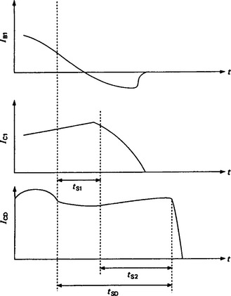
Figure 17.21 The relationship between base current (IB1) the driver transistor collector current (IC1) and storage time (tS1), Darlington current (ICD) and the Darlington storage time (tSD)


Figure 17.23 The reduction of tS2 by means of an anti-parallel diode connected across the emitter-base junction of a driver transistor
The Darlington turn-off sequence is complete after the fall time tfD. This is dependent only on T2 (T1 having been previously turned off). The requirement for optimum turn-off of T2 is dependent on simultaneous cut-off of its emitter-base and collector-base junctions that can be achieved by carefully controlling the value of dIB2/dt.
17.3 Thyristors
The basic thyristor structure is shown as a two transistor analogue model in Figure 17.24(a)). As can be seen from this figure, the thyristor is a four-layer junction silicon device that performs as a controllable rectifier. Functionally, it can be described in terms of two internally connected complementary transistors, with current gains, αnpn and αpnp operative within a positive feedback loop. When the sum of their gains is raised to unity, the forward-biased thyristor switches from a high- to a low-impedance state. In normal operation, current injection through the third terminal or gate initiates this regenerative action. Two-terminal breakover also occurs, as shown in Figure 17.24(b)) by carrier multiplication when the forward bias is increased to a critical value defined as the breakover voltage VBO.
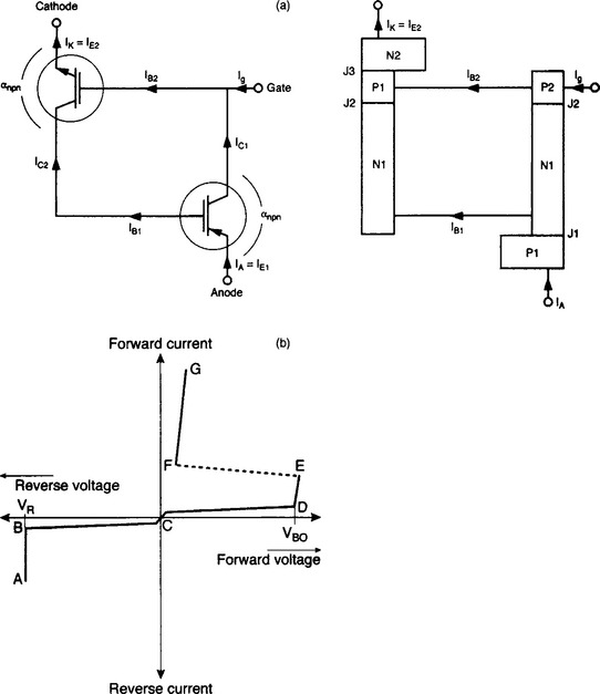
Figure 17.24 (a) Two transistor model of the thyristor; (b) Thyristor current-voltage characteristics
The vertical doping concentrations and the four semiconductor layers of the thyristor are shown in Figure 17.25. Forward- and reverse-blocking voltages are supported across the charge-depletion layers that develop around junctions J2 and J3 of the thyristor shown in Figure 17.25. The vertical layers of the p–n–p–n structure must be designed, therefore, in terms of widths and impurity concentrations to accommodate the depletion regions: this is achieved by the correct specification of the high-resistivity n-type starting material and of the detailed sequential diffusion and fabrication processes used to form the active structure. Under reverse bias, the anode is negative with respect to the cathode and both junctions J1 and J3 are reverse biased. Because the p and n regions at J1 are heavily doped this junction avalanches at a low voltage, and so the device behaves in essentially the same manner as a p–n junction diode, with a low leakage current being maintained up to a critical breakdown voltage.

Figure 17.25 Doping concentration across section of a thyristor. Junction positions J1, J2, J3 are shown
Today, production thyristors are available with voltage ratings up to about 6000 V. Even higher voltages are feasible, but only at the expense of severe de-rating on other important parameters, including current rating and switching speed.
The limit to reverse blocking is set by avalanche multiplication of carriers traversing the high electric field in the space charge region of J3 that occurs at a critical value of maximum field. A wide depletion layer is thus necessary to support a high blocking voltage, and this in turn implies the use of high resistivity, or lowly doped n-type starting material. Although complicated to some extent by the loop-gain, similar considerations apply in setting the level of forward-blocking voltage.
This simple picture is true within the bulk of the thyristor structure, but neglects a factor of crucial importance: this is the termination of the p–n junctions at the silicon surface. Unless corrective steps are taken, electric-field enhancement can occur locally at the surface with a lowering of the breakdown voltage and destructive channelling of the avalanche current. The solution of this problem is by ensuring adequate field relief at the surface. Figure 17.26 shows one approach that can be used, that remains the basis for many of today’s high-voltage ‘alloyed’ thyristors. The edge of the silicon pellet has a compound bevel, with a surface at angle θ1 to the junction plane to control reverse blocking, and a surface at θ2 to control forward blocking. These sections are frequently termed ‘positive’ and ‘negative’ bevels, respectively. The exact measure of the field relief afforded depends on both the diffused concentration gradients and the surface conditions, including the density of surface charge and the dielectric properties of the surrounding ambient. The positive bevel acts by spreading the equipotentials in the high-resistivity n-base region, and a fourfold reduction in peak field is obtained with a bevel angle of about 20°. Likewise, the negative bevel acts by equipotential spreading in the diffused p-region. Its effect is less pronounced and more dependent on the dopant concentration gradient close to the junction. Low-angle bevels, typically 2–4°, are necessary.
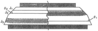
Figure 17.26 Section of a thyristor compound edge bevel. The depletion layer is shown around J3 under reverse bias on the left-hand side, and around J2 under forward bias on the right-hand side
Other types of edge termination are also used on higher power higher voltage thyristors: these include double negative bevels and double positive bevels. These techniques are generally applied to the so-called ‘fully floating’ thyristors. In the ‘alloyed’ device the anode contact is provided by a permanently ‘alloyed’ molybdenum disc, with the cathode contact using being a direct pressure contacted disc. In the free floating type both the anode and the cathode surfaces are contacted using a pressure plate. From the user perspective the alloyed type can offer a better transient thermal response, but it presents difficult manufacturing problems, particularly at high current ratings owing to the large diameter of the alloyed joint. In broad terms devices below 75 mm silicon diameter are more usually alloyed, those of larger size more generally fully floating.
The thyristor conducting area is clearly one key factor in determining the on-state voltage, mean and surge current ratings of a thyristor. Also, when the thyristor is in the on-state, all three junctions are forward biased and the anode-to-cathode voltage drop approaches 1V at low current densities. As the current is increased, additional non-linear voltage drops arise within the base regions, so that the on-state voltage drop becomes particularly dependent on their widths, and the injected carrier lifetime within them. (For a brief description of p–n junctions and carrier injection see Section 17.1.) Both high-voltage or wide-base, and fast-switching or low-lifetime design requirements imply an increase in on-state voltage drop, and hence reduction in current density rating.
The electrical performance of the thyristor is also dependent on the mechanical design and the thermal performance of the housing in which the silicon pellet is encapsulated. Typically high power thyristors are assembled in press pack housings such as that shown in Figure 17.2(a)). But smaller devices use standard stud based or plastic packages. Moving outwards from the silicon pellet, low-resistance non-rectifying contacts must be made to the three electrode regions. As well as carrying the load current without a significant voltage drop, these contacts provide the path for heat flow away from its source within the silicon to an external heat sink or cooling system. This cooling is vital, since all the thyristor characteristics are to some degree temperature sensitive, and the maximum operating temperature of the silicon must be limited to about 125°C. Power ratings depend, therefore, on the thermal resistance between the silicon and the external heat sink, which is cooled by either natural convection or forced-fluid methods. Thermal resistance from junction to mounting base achieved by these techniques ranges from about 3°C/W for a low-power stud-mounted thyristor to below 0.02°C/W for a high-power double-side-cooled encapsulation.
Long-term operational reliability is also a vital feature of all thyristor designs. The packages are hermetically sealed by techniques including electric resistance, projection welding, argon arc welding and cold pressure welding, after thorough vacuum out gassing of all components and filling with a dry nitrogen ambient. The materials used in the packaging are arranged so that the device can withstand many temperature excursions and as a result thyristors can be extremely reliable and survive under extreme conditions for several decades.
It is also possible to deposit a special passivation on the silicon surface, which allows highly reliable thyristor construction in moulded plastic packages similar in external appearance to those used for high power IGBTs (Figure 17.2(b))). An important application of these protected silicon pellets is in assemblies that provide most cost-effective arrangement for many medium and low-power control applications.
The switching behaviour of the thyristor is explained with reference to Figure 17.27 where it is defined in terms of the turn-on and turn-off times, together with the associated dI/dt and dV/dt ratings. The dI/dt rating is the maximum permissible rate of increase of load current, and the dV/dt rating is the maximum rate of rise of off-state voltage that will not initiate conduction.
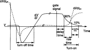
Figure 17.27 The anode-to-cathode and voltage waveforms during thyristor turn-on and circuit-commutated turn-off
The three phases of turn-on are shown in Figure 17.27. The delay time is associated with establishment of transistor, and hence regenerative, action in response to the gate current. Its duration is set by the level of gate drive and by the minority carrier transit times across the transistor bases. A high gate drive reduces the delay time, and wide base regions, or high blocking-voltage rating, increase it. Following the delay time the voltage across the thyristor collapses. Regeneration is well established during the rise time, with charge modulation of the base regions aiding carrier transport so that the rate of current build-up is more rapid. Again, longer rise times are to be expected in high-voltage thyristors with wide base regions, particularly when it is remembered that the collapse of the centre-junction depletion layer during turn-on widens the effective base widths. Finally, there is the spreading time. A fundamental feature of thyristor turn-on is its three-dimensional nature. Because of the finite transverse or sheet resistance of the p-base region, the initiating gate current influences only those regions of the cathode nearest to the gate contact. The gate contact is most usually in the centre of the thyristor. Regenerative switching action is restricted to the turned on regions close to the gate thus formed a narrow conducting plasma. The establishment of the equilibrium current flow over the cathode area follows by outward spreading from this conducting plasma by field-aided diffusion. Plasma spreading is a relatively slow process, with a typical ‘velocity’ of 0.1 mm/μs. When the area of conduction is small the anode/cathode voltage is considerable, leading to high turn on power densities and excessive local heating may result if the current is allowed to increase too rapidly (di/dt).
This turn on spreading phenomenon is affected not only by geometrical factors but also by base widths and such other factors as the recombination rate of carriers within them. The spreading velocity is decreased in both high-voltage and fast turn-off structures.
Where higher di/dt performance is required the amplifying gate structure shown in Figure 17.28(a)) is employed. It may be viewed as the integration of two radially disposed thyristors with a common anode contact. The initiating gate pulse turns on the inner small area, or auxiliary thyristor, this draws current from the external load and provision is made to feed this current back into the silicon via an overlapping metal contact. This amplified current provides the gating current for the main power thyristor. Once the latter is switched, the auxiliary structure is extinguished due to lateral self-biasing voltages. In this way, the repetitive dI/dt rating can easily be increased to about 500 A/μs or greater and switching losses are reduced.

An extension to the amplifying-gate principle is to increase further the area of initial conduction by extending the edge length of the auxiliary thyristor coupling contact and ultimately incorporating an interdigitated gate structure on the silicon surface, as shown in Figure 17.28(b)). The technique is applicable to the highest power large area thyristors. During the on-state all three junctions of the thyristor are forward biased, and both base regions contain excess minority and majority charge. In switching off the thyristor and reverting to the blocking state, charge must either be swept out by an electric field, or decay through regenerative processes within the silicon.
Practical circuits use anode commutation, or bias reversal, to turn off a thyristor, and this is represented by the waveforms as shown in Figure 17.27. When the reverse voltage is applied it forces the current to fall to zero at a rate defined as dI/dt. Once it reaches zero, current flow reverses since the minority carrier concentration at the junctions can support this current as they are extracted before depletion-layer build-up. The peak value of reverse current is reached when the excess hole concentration at the anode junction has fallen to zero. At this time the voltage across the thyristor reverses, with development of the anode depletion layer, and the current decays in a near-exponential manner as a result of charge recombination within the n-base region. It must fall to, at most, the holding current if the thyristor is to block when forward voltage is reapplied. How long this takes is critically dependent on the mean lifetime of injected carriers in the n-base region, and on any extraction of stored charge (in the n-base region) into the load circuit or out from the gate connections.
Special steps are taken to reduce the n-base minority-carrier lifetime in thyristors designed for use in high-frequency applications. Gold, diffused through the structure, or radiation damage is used to provide a controlled concentration of impurity centres or traps through which the injected carriers recombine. Any method used to reduce minority-carrier lifetime leads inevitably to some increase in the on-state voltage drop, principally through a reduction in conductivity modulation of the n-base region. As the recombination centre concentration is raised to reduce the turn-off time, this effect assumes increasing significance, particularly in the case of wide-base, high-voltage devices. The form of the relationship between on-state voltage and turn-off time is illustrated in Figure 17.29.

Figure 17.29 The relationship between on-state voltage (VT) and circuit commutated turn-off time (tq) for fast switching and gold doped thyristors of different n-base width (Wn) and hence different voltage rating
Under normal operation the forward-blocking voltage will be re-applied to the thyristor at a specified rate, or dV/dt as shown in Figure 17.27, and this gives rise to a uniform charge-displacement current as the depletion layer develops around the centre junction. Its magnitude is simply the product of the voltage-dependent junction capacitance, and the value of dV/dt. If no steps are taken to counteract this, the cathode junction will become forward biased by the flow of this displacement current, and this will lead to thyristor switching action.
The so-called ‘shorted-emitter’ technique shown in Figure 17.30 is effective in preventing this two-terminal switching up to high values of dV/dt. It is a method for controlling carrier injection by structural design via a regular array of small-area electrical short circuits in the n emitter to the underlying p region. These ‘shorts’ are usually in the form of an array of distributed dots over the cathode emitter. All high power thyristors use this technique. The displacement current flows laterally to these points and bypasses the emitter regions, this minimises the forward bias developed at the cathode junction. The limit on dV/dt is set by the ohmic voltage drop caused by transverse displacement-current flow in the p-base region. When any part of the cathode emitter is biased above about 0.6 V, it starts to inject and the thyristor may switch on. By correct selection of shorting dot diameters, spacing and array symmetry, dV/dt ratings exceeding 1000 V/μs can be realised without sacrificing much gate-triggering sensitivity. However, some loss in gate sensitivity is inevitable since a fraction of the gate signal will always flow to shorts near to the cathode edge and play no part in the turn-on process. With correct design this can be minimised and the threshold gate current to fire the device kept below a reasonable value of 100–150 mA. There will also be some degradation to the on-state voltage as the emitter shorts give an effective reduction in the cathode emitter efficiency.

Figure 17.30 Distributed shorting of the thyristor–cathode junction to permit high rates of application of forward-blocking voltage or dV/dt rating
From overall design considerations an array of closely spaced minimum area shorts is preferred for a given dV/dt rating. They then occupy the smallest fraction of the cathode area and have the least effect during on-state conduction, and provide the minimum impedance to conduction spreading during turn-on.
The turn-off performance of thyristors can also be improved through the use of increased n-emitter shorting. When the shorting density is in excess of that needed to meet the required dV/dt withstand, forward anode voltage can be re-applied earlier in the charge-decay period, and the residual charge extracted safely from the n base. This is because during turn off the emitter shorts give direct access to the base regions of the thyristor which assists charge extraction and reduces any emitter injection during the turn off period. In this way it is possible to realise high-power fast-switching thyristors for use at frequencies in excess of 10 kHz. A more complete description of thyristors is given in the references 1, 3 and 4 at the end of this chapter.
17.3.2 The converter thyristor
The converter thyristor is designed and optimised primarily for operation at 50 or 60 Hz (mains frequency) and is available up to 5000 V and 3500 A average current rating. The basic design of the converter thyristor is the same as the basic thyristor described above. The introduction of gold or electron irradiation recombination centres is not normally necessary in this type of device, where the main objective of the design is to achieve the lowest on-state voltage possible for the voltage rating required. However many high power applications interconnect several thyristors in series where both static and dynamic voltage sharing is essential between the thyristor levels. In this case it is necessary to achieve an accurate control of the recovered charge during turn off: this control is usually achieved by gold diffusion or radiation damage in a similar manner to that used for fast recovery diodes. As with the fast diode this results in a compromise between low on state voltage, recovered charge, and leakage current.
17.3.3 The fast thyristor
Fast thyristors are designed and optimised for operation frequencies above 400 Hz and up to above 20 kHz. The basic design principles of fast thyristors are the same as those for general thyristors as described above. Their maximum operating frequency is dependent on the switching losses during turn on and turn off, and the turn-off time. The latter is influenced by the intensity of the cathode emitter shorting, the concentration of the recombination centres introduced in the same n-base region, i.e. the minority carrier lifetime, and also by the base width as shown in Figure 17.29. The turn on performance is improved by the use of interdigitated amplifying gates (Figure 17.28), and the use of narrow high gain base regions. As these devices are used under high frequency conditions their safe operation is determined by the impact of switching losses, and the designer requires detailed rating data as shown in Figure 17.31. The frequency-rating curves ((a) and (b)) give the limiting case for operation under a particular forward-conduction duty, to which must be added the reverse recovery losses derived from stored-charge curves (c). From this total average power loss, together with the steady-state thermal impedance, the maximum thyristor case temperature can be determined to retain the junction temperature within its defined rating. Data on the energy dissipation per pulse as a function of pulse base width are also needed to specify the allowable pulse width for a particular duty and an example of such curves is given in Figure 17.31(d).

Figure 17.31 Examples of thyristor square-wave rating data. For ratings tests the gate-source impedance is 10 Ω, with a gate-pulse rise time to 1A of 0.5 μs. The thyristor is switched from 600 V and a resistive capacitive (RC) snubber network of 10 Ω, 0.25 μF is connected
Fast thyristors are available with voltage ratings of 600–3000 V, average current ratings upto 2000 A, turn-off times down to 5 μs and dI/dt ratings over 1000 A/μs.
17.3.4 The asymmetric thyristor
The basic principle of the design of the p–i–n structure which is incorporated in the construction of asymmetric thyristors is similar to the p–i–n diode and is explained in Section 17.1.5. The other features of the basic thyristor structure are retained as shown in the section through an asymmetric thyristor shown in Figure 17.32. In this device, the n-base width is minimised for a particular forward-blocking voltage rating by making use of the limited base-width approach of p–i–n rectifiers and an additional heavily doped n layer is included within the n-base region of the device. As junction J3 is now a p+n+ junction it cannot support a high reverse voltage. By sacrificing this reverse blocking capability which is not required in many applications a significant advantage can be obtained in an improved combination of forward blocking characteristic, on-state voltage and turn-off time. Asymmetric thyristors are available with voltage ratings up to 3000 V, or average current ratings over 500 A and turn-off times down to 2 us.

Asymmetric thyristors may be found in two types, fast turn on and fast turn off. The fast turn on asymmetric thyristor is used in power conversion applications, such as a resonant converter, where the device doesn’t require forced commutation, or turn off. In this case the device can operate at high frequencies, in the 20 kHz and above range, at high power, and most efficiently. A further useful application of such a device is as a pulse power component. The fast turn off device is an extension of the fast turn off thyristor described in the previous section, this type has the advantage of even faster turn off, at the expense of no reverse voltage, and increased manufacturing complexity and cost.
17.3.5 Triacs
The triac, or bidirectional thyristor, was evolved specifically for low to medium current a.c. load control as, for example, in lamp-dimming circuits. Its construction (shown in Figure 17.33) comprises two thyristors in inverse parallel within a five-layer n–p–n–p–n structure. A compound gate region is also included with balanced trigger sensitivities in both the so called first and third electrical quadrants with either a positive or a negative polarity gate bias. The main design problem with a triac is two fold; firstly the two thyristors interact and this will severely limit the turn off and dv/dt capability of the component, and secondly the gates are placed on the same surface, resulting in difficulties in triggering one of the two thyristors. Yet although the triac poses its own set of design compromises, it can be made by conventional all-diffused thyristor processes. In general, triac ratings were limited to about 50 A r.m.s., 800–1000V and of only real use in main frequency applications due to their dv/dt and switching loss limitations but they provide the lowest-cost solution in some a.c. control circuits. For higher power applications, thermal and other considerations make an inverse pair of individual thyristors a more satisfactory proposition.
17.3.6 Light fired thyristors
Light fired or triggering of power thyristors offers the advantage of eliminating the normal gate-firing circuit and overcomes the problems of high-voltage isolation normally associated with gate-firing circuits. Light firing also offers advantages in applications in environments where electrical noise is likely to cause problems by interfering with gate signals.
In the optical-triggering process, the light pulse generates electron and hole pairs. These pairs induce a current pulse that is amplified in turn via an amplifying gate region of the thyristor. This provides sufficient gate current to turn-on the thyristor.
Various light sources can be used such as the light emitting diode (LED) or laser. The light from these sources is pulsed at the appropriate moment into an optical fibre that delivers the light directly to the silicon surface to trigger the thyristor. One of the main problems is the reliability of the light source that is often not as good as the high-power thyristor. Special high-reliability LEDs have been developed for this application. However, although in principle this type of thyristor offers many advantages, it has not been widely used. This is partly because of the limited number of manufacturers who produce this type of device but also because the inclusion of the light-sensitive region on the thyristor adds to the cost and complexity of the device. A more complete explanation of light-fired thyristors is given in reference 3. The main application area for light triggered thyristors was for ultra high voltage electric utility equipment such as HVDC converter stations.
17.3.7 HVDC thyristors
The HVDC thyristor is a special type which although based on the standard converter thyristor structure has several demanding specification requirements. These include high fault current capability, high di/dt, very low on state voltage, a low turn off time, and accurately controlled stored charge. Because generally each HVDC system built is very large, each system design tends to have a specially tailored HVDC thyristor produced for it, using 75–150 mm diameter silicon. The special features that might be incorporated into this type of device are, for example, self-protection in voltage breakover, excess dV/dt, low voltage triggering and light firing. However these features and the highly demanding specification add significantly to the thyristor cost. Therefore such thyristors tend to be too expensive for general industrial applications but are used in other similar applications such as static valve active reactance (VAR) compensation. They are available with up to the highest voltages, e.g. 8000 V blocking voltage and 3000 A average current rating with carefully tailored characteristics.
17.3.8 The gate turn-off thyristor
The gate turn-off (GTO) thyristor has a unique advantage over the conventional thyristor in its ability to be turned off by the application of a negative gate current. Therefore, in applying the GTO thyristor to thyristor inverter or chopper circuits, the forced commutation components are not needed. This offers the advantages of a simpler power-circuit configuration with an associated reduction in cost, volume and weight, less electrical and audible noise, and improved power-conversion efficiency. The GTO revolutionised high power AC motor drives when they became available and were the device of choice for this application prior to the advent of high power IGBT modules.
The GTO is a four-layer p–n–p–n semiconductor device similar in construction to a thyristor but with several design features which allow it to be turned on like a conventional thyristor and off by reversing the polarity of the gate signal. The turn-on action shown in Figure 17.34 is similar to a conventional thyristor. Injection of hole current from the gate forward biases the cathode p-base junction causing electron injection from the cathode, these electrons flow to the anode and induce hole injection by the anode emitter. Injection of holes and electrons into the base regions continues until charge multiplication effects bring the GTO into conduction. As with a conventional thyristor only the area of cathode adjacent to the gate electrode is turned on initially, and the remaining area is brought into conduction by plasma spreading. However, unlike the thyristor, the GTO consists of many narrow cathode elements, such as the device shown in Figure 17.35. This shows the heavily interdigitated cathode and gate region. Therefore the initial turned on area is very large and the time that is required for plasma spreading is small. The GTO, therefore, is brought into conduction very rapidly and can withstand a high turn-on di/dt. This excellent turn on capability also makes the GTO attractive as a fast turn on thyristor for low frequency pulse duty applications.

Figure 17.34 A GTO thyristor during turn-on. Turn-on is initially along the edge of the n+ emitter, the remainder of the emitter is brought into conduction by plasma spreading

In order to turn-off a GTO, the gate is reverse biased and holes are extracted from the p base, as shown in Figure 17.36. Hole extraction continues until the excess carrier concentration is low enough for carrier multiplication to cease and the device reverts to the forward-blocking condition. During turn-off the conducting area is squeezed down to an area remote from the gate electrode and an anode emitter short located in this area to assist turn-off. A lifetime control technique, such as gold or radiation damage is also used to reduce the device p–n–p current gain, thereby improving the turn-off power loss. The switching waveforms that can be observed in the GTO circuit shown in Figure 17.37 are shown in Figure 17.38. Note, the active snubber network consisting of DS Cs and Rs in Figure 17.37 which restricts the dVD/dt that appears across the GTO at switch-off. The meaning of the common terms in the switching waveform are also as shown in Figure 17.38 (td, tr, etc.). The turn-on delay time (td), the rise time (tr), and the turn-on energy (EON) are all strong functions of the magnitude of the gate pulse (IFG) as shown in Figure 17.39. To minimise the turn-on times and energy losses the value of IFG should be as large as possible, consistent with considerations of the drive power loss and cost.
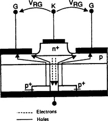
Figure 17.36 A GTO thyristor during turn-off. The gate is negatively biased and holes are extracted by the gate from the p base. The conducting region is squeezed to an area remote from the gate until sufficient charge is extracted to turn the device off


The turn-off of a GTO proceeds in three stages: storage time, fall time and tail time. During the storage time (tgs) the conducting area is reduced due to a squeezing action of the gate drive, and the negative gate current increases to a peak value IGQM. The duration of the storage time depends on how rapidly the excess charge (QGQ) is removed by the gate and is therefore a strong function of the rate of rise of reverse gate current dIGQ/dt. At the end of storage time the anode current falls rapidly, and the reverse gate current begins to decay as the gate junction is forced into avalanche, V(RG)BR. The avalanche condition is not damaging to the GTO thyristor and assists in the removal of stored charge from the device. During this period the blocking junction of the GTO recovers and the anode voltage rises. Unless a snubber circuit (as shown in Figure 17.37) is connected across the GTO the anode voltage could rise at a rate in excess of the device dVD/dt capability and destroy the GTO.
After the fall time tgf, the anode current has fallen to a low value Itail, which decays away more slowly. This tail period is an important factor for the switching losses since the anode voltage is high at this time. In order to reduce these losses GTO thyristors use anode shorting and minority carrier lifetime control to give low values of Itail.
The storage time, fall time, gate turn-off charge (QGQ) and switch-off energy are all functions of the applied negative gate current as shown in Figure 17.40.

In the on state the GTO operates in a similar manner to the thyristor. If the anode current remains above the holding current level then positive gate drive may be reduced to zero and the GTO will remain in conduction. However, as a result of the turn-off ability of the GTO it does possess a higher holding current level than the normal thyristor and, in addition, the cathode of the GTO thyristor is subdivided into small finger elements to assist turn-off. Thus, if the GTO thyristor anode current transiently dips below the holding current level, localised regions of the device may turn off. Forcing a high anode current back into the GTO at a high rate of rise of anode current, after this partial turn-off, could be potentially destructive. Therefore it is usually recommended that the positive gate drive is not removed during conduction but is held at a value IG(on) that is greater than the maximum critical trigger current (IGT) over the expected operating temperature range of the GTO thyristor.
Unlike the standard thyristor, the GTO thyristor does not include cathode emitter shorts to prevent non-gated turn-on effects due to dV/dt forward-biased leakage current. In the off-state of the GTO thyristor, therefore, steps should be taken to prevent such potentially dangerous triggering. This can be accomplished by either connecting the recommended value of resistance between gate and cathode (RGK) or by maintaining a small reverse bias on the gate contact. This will prevent the cathode emitter becoming forward biased and, therefore, sustain the GTO thyristor in the off-state.
Gate turn-off thyristors, or GTOs, are available with repetitive controllable current ratings up to 4000 A and 4500 V forward-blocking voltages. A more complete description of the GTO is given in references 1 and 3.
17.4 Schottky barrier diodes
A Schottky barrier diode, shown for example in Figure 17.41, is based on the formation of a potential barrier by the so called Schottky effect at the interface between a metal such as molybdenum, platinum, chromium or tungsten, and a semiconductor surface such as silicon that is in intimate contact with it. This phenomenon results in the non-linear current transport across the metal semiconductor interface. Forward conduction results from the electrons passing over the potential barrier from the n-type silicon into the metal, reverse conduction is impeded by the formation of a space charge layer. Therefore in conduction very little minority carrier charge is accumulated in the silicon and such conduction is predominantly by the majority carrier electron. The Schottky barrier diode is therefore a unipolar device that operates without the effect of injected carrier modulation. During reverse recovery it behaves almost like a perfect diode switching very rapidly from forward conduction to reverse blocking. This makes the Schottky diode an ideal device for use as a rectifying diode in very high frequency, and fast switching, applications.

In forward conduction the Schottky on-state voltage depends on the contact potential (barrier height) formed between the metal and the semiconductor and, in series with this, the resistance of the semiconducting layers (drift and substrate regions). Because there is no minority carrier injection the on-state voltage is much greater for thicker, and therefore higher reverse blocking, devices. Nevertheless for thin drift and substrate regions the on-state voltage is very low, (for example 0.3 to 0.5 V in silicon) and is therefore significantly better than the p–n diode.
The reverse off-state voltage of the Schottky diode is identical to that of an abrupt p–n junction diode, and is determined by the thickness and resistivity of the drift region. As the reverse voltage rating increases so does the silicon thickness needed to support the space charge region. Unfortunately, the reverse leakage current is also strongly dependent on the Schottky barrier height, and increases as the barrier decreases. This results in the type of characteristics shown in Figure 17.42.

Diffused guard ring structures are usually employed to improve reverse-blocking characteristics by reducing the electric field at the edge of the metal contact area. When combined with an optimised n-type epitaxial layer (Figure 17.41 but guard ring not shown) the best Schottky diode performance is achieved.
Schottky barrier diodes are commercially available with reverse voltages up to 150 V and forward currents of up to 300 A. Higher reverse voltages are prevented in silicon by the high leakage current and consequential operating temperature limitations.
Silicon is not the only semiconductor material that can be used for Schottky barrier diodes, although it is the only material in commercial use at the time of writing. However there is interest in the use of silicon carbide, owing to the high breakdown field and high Schottky barrier height of this type. With further development this will lead to the availability of much higher voltage and higher current Schottky barrier diodes in the future with the potential of higher temperature operation than silicon.
17.5 MOSFET
In the power Metal Oxide Silicon Field Effect Transistor (MOSFET) majority carriers move across an induced channel to carry forward an on-state current. This is better understood by reference to the basic MOS structure shown in Figure 17.43. In this structure the active MOS gate area of the device is on the silicon surface and the MOS gate is made up of three layers: the conductive layer (labelled M which could be a metal), the isolating layer (labelled O for oxide), and the semiconductor layer (labelled S for semiconductor). Layer M is the control electrode or gate. Layer O prevents any d.c. current flow from the gate electrode to the other two electrodes, but does allow the electric field imposed by the gate electrode to influence the surface of the semiconductor. This is how the term ‘MOS’ in MOSFET was originally derived. The MOS device switches on or off depending on the electric field imposed on the p-type semiconductor surface between the two n regions which act as the transistor source and drain regions. If the gate electrode is made positively biased it can induce an inversion layer on the p-zone surface and open a conductive n channel between the two n-type zones. In the on-state the residual resistance in the induced channel determines the level of on-state conduction in the device just below the silicon surface. In the off-state a depleting region is formed at one of the two p–n junctions when a bias is applied between them and the resistivity and width of the p region determines the device voltage rating. This type of structure is limited practically to a few amperes and 50–100V although high voltage types are available for special applications. In more practicable high-power MOSFET structures the semiconductor is exploited both vertically as well as horizontally. One of the two n-doped regions (the drain region) shown in Figure 17.43 is extended to the bottom face of the semiconductor which in effect connects all the elementary structures together forming the drain of the device as shown in Figure 17.44. The p–n junction formed between the channel region and the drain also provides reverse-blocking performance with the depletion region penetrating predominantly into the lowly doped n region. At the same time, because this junction is positioned vertically, it also avoids the waste of horizontal space compared to the structure shown in Figure 17.43 and enables the conductive channel to become very short. To obtain the performance necessary in practicable power MOSFETs this channel is normally designed to be of the order of 1–2 μm. The resulting power MOSFET device therefore consists of multiple-MOS basic cells, with all the n+ type source zones connected in parallel on the top side of the semiconductor chip, together with the gate cells as shown in Figure 17.48. As mentioned above, the substrate of the chip then forms the common drain for the entire multiple source cells on the other side of the chip.


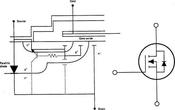
This vertical double diffused DMOSFET silicon gate device described above has evolved to become the design that offers the best combination of characteristics and represents a culmination of the development of the power MOSFET. Because the power MOSFET has evolved and is continuing to develop through various stages of design, it is possible to find several different types in use, illustrated in Figure 17.46 and 17.47.

All these structures have a common feature in that the current flows through a vertical path like conventional high power bipolar devices and, as a consequence, all the devices have two electrodes on the top which are the gate and source, and one on the bottom which is connected to the drain. Another common feature for all these n-channel devices is that the n-region largely supports the applied drain potential because its doping level is much lower than that of the p body region. However, it can be seen that the position of the p channel in the VMOSFET and the UMOSFET differs from its position in the DMOSFET. Although the DMOSFET silicon gate structure needs a more sophisticated technology very similar to that needed to produce CMOS integrated circuits, it is generally possible to produce a far superior device using this process and, therefore, the other three power MOSFET structures are less widely utilised. This is because it can be manufactured using a self-aligned process that makes it far easier to produce. In this process the MOS channel regions are obtained by a difference in lateral diffusion of the two impurity distributions and the use of this double-diffusion technique achieves very short channel lengths of less than 1.5 μm. This increases the potential source/gate packing density that directly reduces the cost and improves the performance of the device. At the same time the use of a polycrystalline gate also reduces the possibility of sodium ion contamination in the gate oxide, and results in a higher stable threshold voltage VGS(th).


However the UMOSFET structure has recently been given increased attention as fabrication techniques have improved to a degree that it could be practically realised. This type of MOSFET device is also referred to as a Trench MOSFET, and correspondingly the DMOSFET is called a planar MOSFET. The advantage of the Trench MOSFET is the capability to achieve far greater cell packing densities, but at the expense of increased manufacturing difficulty.
As mentioned previously, the n-MOSFET structure is switched on by applying a voltage between the drain and the source and positively biasing the gate with respect to the source. This bias creates an electric field in the channel region that reverses the polarity of the charge carriers in the body region to create a majority carrier path from the source to the drain. Electron current flows from the source metal to the source contact, laterally through the channel and then vertically through the n− and n+ drain regions to the drain contact as shown in Figure 17.44. This structure also contains an internal parasitic diode, formed by the source short-p body contact, and a bipolar n–p–n transistor as shown in Figure 17.48.
The diode conducts when the drain is negatively biased with respect to the source and usually can conduct forward current at the same level as the MOSFET part of the device. Under these conditions charge is injected into the n-region and the parasitic diode behaves almost like the epitaxial fast-recovery p–n junction power. It does, however, suffer from the disadvantage that it cannot be made a very fast-recovery type, as normally required for high frequency MOSFET applications, without affecting the other characteristics of the MOSFET. Therefore, although it can be used in certain lower frequency applications as an internal inverse parallel diode, this is often avoided by inserting an external reverse blocking diode in series with the MOSFET and providing another inverse parallel to carry reverse current. Where the internal diode is used an allowance must be made for the additional power losses dissipated in the MOSFET structure and the parasitic diode’s reverse recovery characteristics resulting in a reduced power rating and/or a lower permissible switching frequency. The advantage in using the internal diode is of course the elimination of the two external components. Where it is essential to use the external diodes they should be of the very fast-recovery type such as a Schottky barrier diode, or a fast switching p–n diode, to keep switching losses in the MOSFET to a minimum.
If the current flow in the diffused base resistance in the p+ region of the parasitic transistor shown in Figure 17.48 (which may be very high under MOSFET current conditions) is sufficiently large, the p+−n+ emitter junction of the parasitic transistor will become forward biased. This injects current that will be conducted by the parasitic n–p–n transistor. Usually only a few of the MOSFET cells reach this condition first wherein a very high current is focused that destroys the device. This is one of the basic failure mechanisms of the MOSFET that is avoided by preventing the load current of the MOSFET exceeding a critical value. The critical value of current also decreases with increasing temperature but is usually well beyond the manufacturer’s rating specification. However it is a mechanism which should be borne in mind together with the fact that a MOSFET does not have the capability of passing an unlimited amount of current for a very short time.
To minimise on-state power losses in a MOSFET the device on-resistance (RDS(on)) needs to be the minimum compatible with desired breakdown voltages. To achieve the maximum possible (RDS(on)) it is necessary to optimise the power MOS channel perimeters to achieve the highest packing density per unit area possible. As a result, planar DMOS low-voltage devices have a packing density of 1000–10000 cells or more per square millimetre This has resulted in the development of advanced ‘Trench’ MOSFET structures which can reach even higher cell densities up to 20 000 cells per square millimeter. For high-voltage devices the epitaxial layer resistance has a greater effect on the overall resistance and to optimise (RDS(on)) it is necessary to minimise the bulk resistance by choosing a lower packing density which increases the area of the epitaxial drift region. High-voltage devices therefore often have a packing density of about 500 cells per square millimetre. Many novel techniques have been considered for reducing the epitaxial drift region resistance, with such proprietary names as ‘CoolMOS’.
The maximum breakdown voltage rating of the DMOSFET (BVDSS) would be limited by junction edge breakdown effects below the bulk avalanche breakdown due to the curvature of the diffused junctions and surface electrical field crowding, unless an edge structure such as that shown in Figure 17.49 is used. The field plate allows higher breakdown voltages by spreading the field laterally along the surface of the device.

The gate threshold voltage (VGS(th)) is another important parameter. This is the voltage at which strong inversion begins to occur in the MOS gate and sets the minimum applied gate voltage for conduction in the channel. The threshold voltage is related to the thickness of the gate oxide and to NA, the maximum peak impurity concentration in the region between the source and the drain. Channel punch-through can occur as the result of insufficient impurity charge in the channel, under strong reverse bias and to avoid punch-through a trade off between VGS(th) and length must be made. Due to the negative temperature coefficient of VGS(th) its value cannot be allowed to become too low otherwise the gate becomes too sensitive at high temperature. Also, if it becomes too high, the MOSFET cannot be directly driven by low-voltage logic circuits or requires too much gate power and, therefore, the value of VGS(th) is normally designed to be in the range 2–4 V for power devices, although lower values of 1–2 V are found for logic-compatible devices
Power MOSFETs require a certain amount of gate charge driven into their gates or extracted during the charging and the discharge phases of the input capacitance and behave quite differently from bipolar devices. In particular the switching performance of the device is influenced by the time it takes for the voltage to change across the device capacitance. Figure 17.50 show a power MOSFET driven by a gate source with an internal resistance R1 and an open-circuit voltage V1 where RL is the load in the main switching circuit.

The gate input capacitance CGi = CGS + CGD is nonlinear during the switching cycle. The capacitance between the gate electrode and the drain CGD is a function of the depleted drain layer thickness which in turn is dependent on VDS (drain source voltage). As VDS increases the depleted layer thickness increases and the static input capacitance CGD decreases.
There is also a displacement charge which has to be supplied when VDS decreases from VDD to VDS(on) and CGD behaves as a higher equivalent capacitance than during the drain ‘on’ transitions. CGD is called the Miller Capacitance and it causes the total input capacitance to exceed the sum of the static capacitance during the dynamic turn on phase.
During the turn on period the voltage across the gate increases until it reaches the threshold voltage (VGS(th)), at this point drain current begins to flow and CGS becomes charged. When the gate source capacitance is fully charged, the drain voltage begins to fall while the drain current is almost constant charging the Miller Capacitance CGD. During this phase the VGS is also constant, as it cannot increase until the input capacitance is fully charged. This is the so-called Miller effect. Following this VGS increases again until it reaches the gate supply voltage Vi.
The minimum charge that must be delivered by the gate drive to ensure turn-on is therefore given by the charge required to fully charge the input capacitance, however in practice gate drive design will require the use of greater capacity so that the gate voltage reaches the gate supply voltage, i.e. time t4 in Figure 17.51.

At turn-off, the behaviour of the input capacitance is exactly opposite, and the phenomena described above occur in reverse order.
Power MOSFETs are available with current ratings up to 200 A and voltage ratings to 1000 V and are capable of switching at frequencies up to 10 MHz. The high switching speed, wide SOA, high peak current capability and ease of control has made the power MOSFET the favoured device for the majority of power electronic applications. Unfortunately it is the unipolar operation of the device, that delivers the above benefits that also leads to highly temperature and blocking voltage dependent conduction characteristics, and therefore restrict the useful application area to the lower power regime. A more complete description of the MOSFET is given in reference 2.
17.6 The insulated gate bipolar transistor (IGBT)
In searching for the ideal power device, designers have considered many potential design concepts that combine the voltage control of the MOSFET gate with the superior conduction characteristics of the bipolar device. Of the many candidates there is only one that has become widely commercially available, the insulated gate bipolar transistor (IGBT). There is much research and development work in hand to implement improved versions of the IGBT, for example incorporating Trench Gates and making use of accumulation layer emitter effects, however this falls outside the scope of this chapter where we will focus on the commercially available DMOS IGBT. The IGBT employs injected-charge modulation in the base region and, due to the need for this charge to be extracted or extinguished at turn-off, has higher switching losses compared to the MOSFET. But as it can be realised at much higher power ratings it has become the power device of choice for a wide range of medium to high power electronic applications. The main advantages of the IGBT are the simplicity with which it can be driven (which is comparable to a power MOSFET), its lower on-state conduction losses and the capability of switching high voltages. These characteristics, together with the ability of IGBT to survive a wide reverse bias safe operating area (RBSOA) make it superior to the power MOSFET in high-voltage applications. Typically, IGBTs are used for switching circuits requiring high voltage (up to 3300 V) and high current (up to 3000 A), with a switching frequency of the order of 1–40 kHz.
17.6.1 Device physics
Figure 17.52(a) shows a cross section through a single cell of the multi-cell structure of an IGBT and Figure 17.52(b) shows the power MOSFET for comparison. The drain region of the IGBT which contains a p+ doped layer represents the major difference in structure to that of power MOSFETS. The presence of the p+−n junction drastically reduces the on resistance of the IGBT during conduction because holes are injected from the p region, which results in the n− region becoming conductivity modulated. In a power MOSFET significant proportions of the conduction losses occur in the n− region, for devices above 500 V this can amount to more than 70% of the total.

As is also shown in Figure 17.52 the Source of the MOSFET becomes the Emitter of the IGBT, and the MOSFET drain has become the Collector. This change in terminology correctly demonstrates that the IGBT is a bipolar device and that the effective ‘Drain’ of the MOSFET section is not directed connected to the external circuit.
A circuit model of the IGBT, shown in Figure 17.53(a), illustrates the internal arrangement. The MOS section provides a gate drive to the base of a p–n–p transistor (formed by the p+n+n−p+ layers in Figure 17.52(a)) where in this p–n–p transistor its emitter is directly connected to the IGBT collector and the p–n–p collector feeds into the base of a second n–p–n transistor (formed by the n−p+n+ layers). Thus it can be seen that the IGBT resembles a four layer n–p–n–p thyristor structure, see the two transistor analogue of the thyristor in Figure 17.24. In this thyristor analogy the gate drive to the thyristor derives from the MOSFET gate. As with the thyristor, should the sum of the n–p–n and p–n–p gains (αnpn + αpnp) exceed unity then the IGBT will latch on, as a thyristor, with consequential loss of gate control and potentially destruction of the device. In order to prevent latch up IGBTs are designed to achieve control over the gains αnpn and αpnp. This gain control is usually achieved by three approaches. Firstly the resistance RB is minimised (this is analogous to efficient cathode emitter shorting in the thyristor, see Section 17.3.1 and Figure 17.30). Secondly the injection efficiency of the p+ layer (at the collector) is reduced by various techniques, for example the structure in Figure 17.52(d) uses an n+ layer. Finally, the p–n–p gain may be reduced by minority lifetime control.

With the above mentioned techniques to de-sensitize the ‘thyristor’ action of the IGBT, the NPN transistor may be ignored and the equivalent model is simplified to that shown in Figure 17.53(b). In both models Rmod represents the effective resistance of the n− region in the ‘drain’ region of the device (i.e. the MOSFET region drain). Referring to Figure 17.53(a) or (b) the drain region of the IGBT is the region in the centre below the gate, in this region the n-base region is surrounded by p-base regions. In the forward biased condition, and when the IGBT is conducting the p–n junction between the p- and n-base is reverse biased. Thus this reverse biasing effect may increase the effective resistance Rmod. As a result many IGBT designs take particular care to maximise the conductance in this region of the device by increasing the n-type doping in this region for example. In some equivalent circuit models this is shown as a JFET (a Junction Field Effect Transistor) because the p+ base regions surrounding this n− drain act as the junction of a JFET structure. For an explanation of the JFET see reference 5.
There are two major types of IGBT manufactured, either Punch-Through (PT) or Non-Punch-Through (NPT). The IGBT structure shown in Figure 17.52(a) is a PT IGBT and this has the similar structure to the Power MOSFET with the addition of the p+ layer (Collector) to the drain side of the MOSFET. In this structure the off-state voltage is supported by the formation of a space charge region across the wide n-region, but this space charge region punches through to the n+ buffer region before the junction breaks down. In this respect it is similar to the p–i–n junction (Section 17.1.5) in that it achieves a thinner device structure, and therefore minimum on-state voltage and improved dynamic characteristics, for the same blocking voltage.
In an NPT IGBT structure the n+ buffer layer is omitted, and so the thickness and the doping levels in the n− region are chosen such that the junction breaks down before the space charge region reaches through to the p+ collector region.
The choice between NPT and PT types is based on a number of factors surrounding the manufacturing process cost and yield and the IGBT characteristics. In the earlier IGBT types PT has been restricted to IGBTs at voltages less than 1200 V owing to the economics of growing the very thick epitaxial layers needed for higher voltages, but many manufacturers have developed both PT and NPT types across the full voltage range.
As with the Power MOSFET the IGBT is available in both DMOS and UMOS (or more usually ‘Trench Gate’) construction. The Trench gate is generally used in the high power IGBT to improve the effective conduction area of the IGBT and reduce the VCE(on), although it can also be used to increase the cell packing density to improve the switching speed for lower voltage designs. At the time of writing the trench IGBT was just becoming commercially available at 1200 V levels with higher voltage designs in development, whereas the DMOS device is available up to 6500 V.
17.6.2 Packaging and thermal considerations
Although IGBT are available in discrete packages, i.e. packages that contain one IGBT die, the majority of IGBTs are supplied in module configurations. A module is a package that contains more than one IGBT die, and may more usually contain a combination of IGBT and fast recovery diode die. An example of a high power IGBT module, with one half of the lid cut away to illustrate the internal construction, is shown in Figure 17.56.

Typically the module has a conductive base plate of copper or alternatively a metal matrix material (such as AlSiC), the IGBT and diode die are soldered onto a DCB and one or more DCBs are soldered to the base plate. The DCB (Direct Copper Bonded substrate) consists of an insulating material, such as Aluminium Nitride or Alumina, with a copper layer bonded to both sides, and with the side to which the die are attached patterned to produce the necessary interconnections between the die. The DCBs may be further interconnected within the module and the main terminal electrodes (cathode, anode and gate) are connected to the DCBs. Clearly the detailed design and construction of the module is extremely complex and requires consideration of the electrical, thermal (for high transfer) and mechanical requirements. Of prime importance is the reliability of the package, and manufacturers go to great lengths to optimise the life expectancy of the module.
The IGBT module will contain fast recovery diodes connected across the IGBTs, in anti-parallel. The inclusion of the diodes results in ease of assembly and low parasitic inductance to optimise the switching and operating area of the module. The diodes used in the modules are of the fast-recovery type but are specially designed to have soft-recovery. The use of soft-recovery diodes is essential in order to prevent the snappy recovery of the diode applying excess voltage stress on the IGBT at turn on.
In the assembly of equipment using IGBT modules the user usually connects to the power terminals by parallel busbar rails and the layout of the power terminals facilitates the use of extremely low inductance rails. The base of the module is connected directly to a heaksink surface and because the base plate is electrically isolated from the IGBT die several modules may be mounted side by side on the same heatsink. Thus the IGBT module lends itself to ease of assembly and extremely compact equipment designs.
17.6.3 On state characteristics and conduction losses
Current flow in the IGBT during conduction is shown in Figure 17.54. The total current IDS is the sum of the two currents IC(h) and Ib(h), where Ic(h) is the current due to holes injected from the substrate p+ layer, which are collected on the surface of the source region, and Ib(h) is the current due to holes that combine with electron current flowing through the MOS channel in the base region of the p–n–p bipolar junction transistor. The IGBT, therefore, behaves like a bipolar junction transistor whose base current is provided by a MOSFET, and the drain current of the IGBT is thus the sum of the bipolar base and collector currents.

From this it can be seen why the IGBT has a higher current carrying capability and lower RDS(on) than a power MOSFET of equal chip size. However, the presence of the p+−n junction in the drain produces an initial offset in the output characteristics of 0.6–0.8 V, and also limits the reverse breakdown voltage of the IGBT to 30–70 V. However for most applications (e.g. voltage source inverters) the lack of reverse blocking capability is not a problem.
17.6.4 Turn on and turn off
When the gate-source voltage (VGS) is greater than the threshold voltage (VTH), the MOSFET section of the structure turns on. The MOS drain current is then the base current of the parasitic p–n–p transistor and it turns on the p–n–p transistor in less than 100 ns. The IGBT turn-on time is therefore, a function of the impedance of the gate driver circuit and the voltage applied to the gate. During this turn-on time the falling voltage and rising current can result in high instantaneous power levels, leading to a total energy loss during this phase, called the turn-on switching loss.
Turn-off in the IGBT has typical features of both a power MOSFET and a bipolar junction transistor turn-off due to the use of conductivity modulation for increased current density. Figure 17.55 shows how the turn-off can be divided into four regions, during the first phase (I) the gate voltage decreases to a point where the Miller effect begins and VDS begins to rise. In the second phase (II) the gate voltage is constant due to the Miller effect. During this period the gate capacitance decreases as VDS increases. The gate voltage polarity is reversed with respect to the drain voltage, as VDS rises above the gate potential and VDS rises to its maximum value at a rate controlled by the driver circuit. These two phases (I and II) are dependent on the MOSFET behaviour as the base-collector junction of the p–n–p transistor becomes reverse biased. Regions III and IV define tfall. In region III the turn-off process is MOS controlled which is very fast. In region IV the MOS channel is closed and the p-n-p transistor has an open base. During this period the current falls at a rate determined by recombination of excess carriers in the n− region. The fall time can therefore be controlled by the gate drive-circuit, in region III, but in region IV is only dependent on the -p-n-p transistor lifetime and gain. Figure 17.57(a) shows how tfall varies with VDS. It can be seen that, as VDS increases, so the gain of the p-n-p transistor increases due to the reduction in the base thickness. This is caused by the depletion region increasing with increasing VDS. The dependence of tfall on temperature is shown in Figure 17.57(b) and confirms the correlation between tfall and the p–n–p transistor gain. The lifetime of the minority carriers in the n− region versus tfall is shown in Figure 17.57(c).
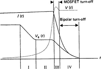

17.6.5 Safe operating area
Protecting the IGBT against over-current or over-voltage effects that can be potentially destructive is a most important part of the design for the majority of applications. These can be specified by the ability of the device to withstand a short circuit load, the short circuit safe operating area (SCSOA) and to survive during switch off, the turn-off switching safe operating area (SOA).
The SOA is illustrated by considering the switching of an IGBT in a half bridge circuit shown in Figure 17.58. The switching waveforms are shown in Figure 17.59. The SOA curve is derived from the locus of maximum permissible current and voltage during the turn off phase, for example Figure 17.60. The failure mechanism is typically due to the rapid extraction of charge from the bipolar section of the IGBT, this charge may flow laterally in the base regions and can lead to latch up of the equivalent thyristor section of the device.


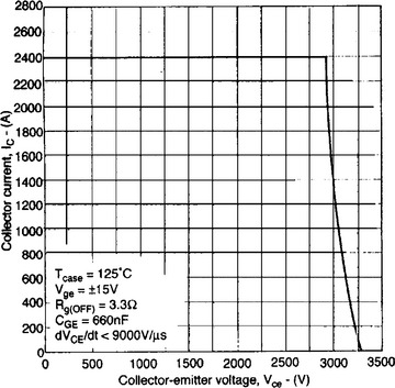
In many applications it is important that the IGBT can withstand a short circuit event in the system, for example in the motor. The are two situations that may occur. Firstly where the IGBT is turned on into a short circuit Figure 17.61(a). In this case the IGBT is initially off and supporting the supply voltage Vcc, the IGBT is turned on into a short circuit where the only load is the stray circuit inductance Ls and the IGBT voltage then drops due to the discharge of the stray inductance and then rises rapidly back to the supply level. This rapid dv/dt is picked up by the gate due to the internal capacitance of the IGBT, and this rise in gate voltage results in a further increase in the collector current. In this condition the IGBT must be turned off within a defined time of the order of 10 μs, and the peak over-current should be limited or the device will fail.

Figure 17.61 IGBT switching waveforms under short circuit conditions: (a) IGBT turned on into a short circuit; (b) load short circuited while IGBT is conducting
The second condition for SCSOA is where the device is already in conduction when the load is made short circuit. Figure 17.61(b). The short circuit forces the IGBT into de-saturation, the collector voltage rises rapidly towards the supply voltage Vcc, as in the previous example this dv/dt forward biases the gate strongly leading to higher values of collector current. Again the peak collector current and the duration of the short circuit must be limited to avoid device failure. Most manufacturers will define the conditions to limit SCSOA in their data sheets.
IGBTs are available covering a broader spectrum of power than almost any other power device, with the exception of the thyristor. IGBTs are available from a few amps and 300 V up to 3000 A and 6500 V. These devices are used over a broad frequency range from a few hundred Hz up to and exceeding 100 kHz. At the time of writing no suitable alternative has been released that might challenge the dominance of the IGBT, but there is no doubt that as this device technology becomes mature the device designers will turn their attention beyond the IGBT. For further reading a more complete description of IGBTs is given in reference 2.
Acknowledgements
Much of this text is derived from the first edition prepared by Dr Roger Bassett when he was Marketing Manager for what was to become the power business of Dynex Semiconductor Ltd in Lincoln England, but was at the time owned by GEC Plessey Semiconductors. The recent revisions and additional material are included with the kind permission of Dynex Semiconductor Ltd.
1. Ghandi, S.K. Semiconductor Power Devices. Wiley; 1977.
2. Williams, B.W. Power Electronics, Devices, Drivers and Applications. New York: MacMillans Education; 1987.
3. Taylor, P.D. Thyristor Design and Realisation. New York: Wiley; 1987.
4. Benda, V., Gowar, J., Grant, D. Power Semiconductor Devices Theory and Application. New York: Wiley; 1999.
5. Baliga, B.J. Modern Power Devices. New York: Wiley; 1987.