Semiconductor, Thick and Thin-Film Microcircuits
W Eccleston, MSc, PhD, CEng, FIEE, University of Liverpool (Section 6.1)
D Grieve, BSc, Welwyn Components, Bedlington (Section 6.2)
6.1 Silicon, silicon dioxide, thick- and thin-film technology
Silicon is unrivalled as a semiconductor material for active devices such as rectifiers, metal oxide semiconductor field effect transistors (MOSFETS), bipolar transistors, thyristors and a wide variety of other structures particularly designed for power applications. Few of the properties of silicon are ideal but none are so far from ideal as to exclude its use in all but a small fraction of current devices. Perhaps the most important application where it is excluded is in the generation of electromagnetic radiation, optical infra-red or microwave. Such emitters usually require a material where electrons can lose energy directly with emission of light rather than by interaction with the lattice of semiconductor atoms. For this application a variety of compound semiconductor materials are available such as gallium arsenide and gallium phosphide. Much research is, and has been, focused on producing optically emitting alloys of silicon with other elements such as germanium which can be integrated on a silicon substrate using the existing highly developed technology.
6.1.1 Materials for integration
Quite fundamental to silicon technology is the existence of a natural oxide which can be produced thermally in oxygen or steam and which is hard, uniform in thickness, has an acceptable value of relative permittivity (3.9) and high electrical breakdown field strength (2 × 10⁷ Vcm−1). Many semiconductor devices have at the surface electron densities of between 1011 and 1012 cm−2. It is important that these carriers remain mobile, rather than being trapped at spare or dangling bonds at the interface between the single-crystal silicon and the amorphous oxide with its much more randomly oriented atoms. Less than 1% of the silicon atoms should have such a bond if an acceptable number of electrons is to remain mobile. This can be achieved through hydrogen treatment at temperatures below 650°C. Too high a level of trapping leads to devices of low gain and high electrical leakage.
Silicon dioxide is near ideal for carrying thin-film conductors from and to adjacent regions of active devices. When it contacts silicon, however, to make an ohmic contact it will take it into solid solution, essentially etching the silicon. Spikes of aluminium, with dissolved silicon, occur which may short out the device. For this reason aluminium already doped to the level of solid solubility with silicon is used for the starting material. Contact to the package is made with aluminium wire which is ultrasonically welded to thick aluminium pads on the silicon dioxide. The bond-wire is also doped with silicon. Polycrystalline silicon also serves as a current carrier on integrated circuits. Impurities such as phosphorus and arsenic are used to dope the polysilicon and this renders it much more conducting. Its conductivity can also be improved by converting it to one of the silicides of metals such as platinum, cobalt or tungsten. Silicon dioxide must be etched to allow the conductors on its surface to reach the underlying active regions. These holes in the silicon dioxide are required to be as small as possible, of ‘minimum feature size’, and methods of etching it employing either gaseous or aqueous fluorides have been developed.
There is considerable advantage in having an insulating layer buried beneath the transistors. Device capacitance is reduced as is a wide range of spurious transistor latch phenomena which can destroy the transistors. Silicon dioxide is used in the form of a thin film, often implanted into the silicon. This kind of implantation requires very high current densities, followed by annealing at temperatures of 1350°C, when there is a condensation of the oxygen ions to produce a layer of not very dense silicon dioxide. Wafer bonding is also used for this application. Two oxidised wafers are bonded together by heating the two oxidised surfaces in contact. One of the slices is then etched back to produce a thin film suitable for devices. An intriguing technology is that of porous silicon. The slice is anodised in hydrofluoric acid, when the selected regions acquire a large number of microscopic holes which are later oxidised to produce silicon dioxide. Porous silicon also has possible applications for light-emitting devices. The presence of pores substantially modifies the electronic properties of silicon, the confined electrons being able to fall through large energy differences without interaction with the lattice of silicon atoms. A particular problem of this type of technology is the very poor thermal conductivity of the oxide. Power dissipated in the silicon islands containing the devices produces temperature rises of the order of 150°C. An earlier form of ‘silicon on insulator’ employed sapphire as substrate, partly because of its crystalline structure but also because of its high thermal conductivity.
6.1.2 Silicon and impurities
The devices produced in silicon depend for their properties on the addition of very low concentrations of impurities coming from group 3 or 5 of the periodic table. The silicon atom belongs to group 4 and it bonds in the single crystal in a tetrahedral configuration with each atom having four nearest neighbours. This configuration gives the material its brittleness which can be a problem when it is being handled. The lattice constant is 5.4 A which is the length of the side of the cubic unit cell. Group 5 elements such as phosphorus and arsenic have five outer electrons available for bonding, leaving one electron unused and in orbit. The application of Bohr theory to such an orbiting electron is justified as long as the effect of the crystal is taken into account via the use of the effective mass of the electron and the relative permittivity (12) of the silicon. The calculated radius of orbit is very much larger than the lattice constant and the electron is only very weakly held. Thermal vibrations of the lattice can easily shake the electron loose at room temperature and it can then contribute to the conductivity. Suppose 1016 cm−3 of phophorus atoms is added to an otherwise pure crystal (an impurity level of 1 ppm). The electron concentration is increased from 1.5 × 10¹⁰ to 1016 cm and the conductivity is increased by approximately 106. This remarkable change is the basis of the usefulness of impurities in producing semiconductor devices.
In order to consider the effects of substituting group 3 atoms for silicon it is necessary to understand the nature of electrical conductivity in single-crystal solids. Bohr theory describes the properties of the isolated atoms in terms of electrons in orbit around a positive nucleus. When isolated atoms condense to produce a solid we must also apply the Pauli exclusion principle which states that the electrons must each have a different orbit. Instead of a single energy level of the Bohr model we have bands of levels each containing the same number of energy levels as the number of atoms. The free or conduction electrons fit a similar model. When an applied field acts on an electron it will increase its kinetic energy and move it to a higher level, but it must still obey the exclusion principle. A consequence is that no conductivity can take place in a full band. In a semiconductor the highest filled band at 0 K is called the valence band; the first unfilled band is the conduction band. At higher temperatures some of the electrons in the valence band will be able to jump across the energy gap leaving behind a few vacancies in the valence band and giving some free electrons in the conduction band. At 300 K the number of such electrons in the silicon is the intrinsic carrier concentration. The presence of vacant energy levels in the valence band provides an additional form of conductivity since the sea of electrons in this band can experience an overall gain in energy and, because the band has an electron deficiency, it can be ascribed a positive charge. The total conductivity of all the electrons is equivalent to that of a single positively charged particle. We term this a hole. The intrinsic hole concentration is therefore equal to the concentration of electrons in the conduction band since, as expected, the material remains electrically neutral.
When a group 3 atom substitutes for silicon it is short of an electron to complete all the bonds to the four nearest neighbour silicon atoms. This electron is gained from the valence band, leaving a vacancy and the remaining electrons can contribute to the conduction. A hole is therefore created.
Two types of material can therefore be created by the addition of impurities. Group 5 elements become positively charged fixed centres which release electrons making the material n type. Group 3 elements take up an electron from the valence band leaving behind a mobile positive hole and the material is then said to be p type. The intersection of a p-type material with an n-type one gives rise to a p-n junction which is a rectifier but is also the building block of almost all other semiconductor devices.
Impurities can be added to the melt during the growth of the single-crystal material. This process involves pulling a seed of the crystal from the melt whilst also rotating it. A long single crystal is so produced up to 8 in. diameter. This is sawn many times along the same well-defined crystal plane and each resulting slice is ground and polished on one of its two faces. The doping level and, therefore, the resistivity can be controlled to within a few per cent of the desired value. In most cases later doping during device fabrication will overdope this background level. Such impurity atoms can be introduced from a solid or gaseous source in a furnace at temperatures in the region of 1000°C. Patterning silicon dioxide guarantees that the surface of the slice will only be doped in the areas required. This stage is termed the predeposition stage. In order to get the atoms on the desired silicon sites it is necessary to heat the silicon for a prolonged period in the absence of the dopant. This is termed the drive-in stage and must be carried out in an oxidising atmosphere in order to produce a layer of silicon dioxide on the surface of the silicon, sealing in some of the impurity. Even with this precaution a large amount of impurity is lost. The final depth of the p-n junction will be much deeper than that after the predeposition. A major difficulty with this technology is that the spread in the resistance can be as high as 20%, which is unacceptable for the more advanced processes. Better control is achieved by ion implantation. Here a beam of suitably charged ions delivers a closely monitored number of ions to the surface. The ions are energetic and much surface damage is caused. The ions sit interstitially in the silicon and must be activated by prolonged annealing. Control is greatly improved but the cost of a commercial implanter is high. The process is essentially serial and, therefore, time consuming, in contrast to diffusion where many slices of silicon can be loaded into a furnace for simultaneous predeposition. Control of the temperature-time cycle is difficult with simple furnace processing and a ramped temperature cyle is increasingly used. This factor is of great importance in very low dimensional structures since any unnecessary heating during the warm-up period produces an unwanted lateral spread of the impurities and loss of dimensional control. For this reason a well-controlled temperature cycle is employed giving precise control of geometry. This is a single-slice process and is often termed limited reaction processing. Batch processing is less popular since it can, on equipment failure, lead to the loss of expensive part-processed wafers.
In a small but significant number of cases it is necessary to produce a layer which is less heavily doped than the background of the crystal. This is done using epitaxy. Silicon tetrachloride, dichlorosilane or silane is decomposed at high temperature (1200°C down to 900°C). The resulting silicon atoms which have high mobility on the silicon surface are able to migrate to appropriate crystal sites, reproducing the orientation of the underlying silicon. Gaseous dopant is added to the gas stream and can be varied in type and concentration during the growth. The high temperatures required in the reactor guarantee high atom mobility and good crystal quality; however, they do lead to short growth times and relatively poor thickness and doping control, particularly across a slice. The reactor consists of a cold-wall vessel which prevents unwanted deposition of material, and heating either with radiofrequency in small-scale systems or lamps in large commercial apparatus.
6.1.3 Mobility and the materials limitations of device size
Throughout the history of silicon circuit development there has been a particular emphasis on making devices, and hence circuits, smaller. This need is associated with the statistics of defect creation, both in single-crystal silicon and in the associated silicon dioxide and conductors. The fraction of working circuits increases in an exponential fashion with decreasing area of silicon and the cheapness of producing the finished chip follows, therefore, a similar very sharp function.
Producing the windows for selective addition of impurities is a critical process which utilises a photosensitive liquid spun on the surface, and after heat treatment is exposed through a photomask to produce the desired pattern. The silicon dioxide can then be etched to leave windows of exposed silicon. Alternatively, a material can be applied to the surface which is chemically sensitive to electron beams. A scanning electron beam can be used to define features in this ‘resist’ layer, which masks the surface in selected areas during a subsequent manufacturing process. As the physical dimensions of transistors are reduced, the electric-field strength in the silicon and the silicon dioxode becomes very high. At low field, the drift velocity of the electrons, or holes, depends linearly on the applied field. The rate of change of velocity with field is the mobility. Reducing the chip supply voltage in proportion to the device dimension should be possible without degradation of speed of operation. Unfortunately, as the intensity of the fields becomes higher the velocities of the electrons become field independent, mobility falls and circuit designers are forced to drive the circuits harder by maintaining a high supply voltage, typically 5 V. The silicon shows carrier multiplication through hot electrons or holes exciting other electrons and holes, by collision, across the energy gap. Modern circuits are often so complex that adjacent n and p regions form unwanted four-layer thyristors which can switch into a state where very high currents can pass. The same carrier multiplication can generate white light. Long-term degradation of silicon dioxide is known to be associated with the generation of very energetic carriers in very small transistors where the electric field strengths are very high.
6.1.4 Materials for large-area circuits
The prime limitation on the production of large-area circuits is the very strong relationship between the fraction of working circuits and the defect density. Attempts at wafer-scale integration (WSI) have been made. This is an attractive possibility in that it reduces packaging costs and the overall size and weight of equipment. Clearly, to overcome the problems of the relationship between yield and area it is necessary to build in large amounts of redundancy through the duplication of power lines and circuits. There is little materials technology which is specific to this kind of circuit.
Although single-crystal silicon slices have increased in area and have fallen in cost over the years, they are still impractical for some applications. In some cases it is possible to get satisfactory performance from devices made in silicon on glass or other cheap flat substrates. Silicon deposited at room temperature is usually amorphous. It has randomly oriented atoms and thus a large number of dangling bonds which can be taken up by treating the film with hydrogen. Dopants can be introduced during growth and relatively poor p-n junctions are obtained. The energy difference between conduction and valence bands is larger than for single-crystal silicon and this reduces leakage currents. A major course of such leakage is the excitation of electrons from the valence band to the conduction band which becomes less probable with a larger energy gap. Amorphous silicon can be very photosensitive and the availability of large areas on panes of glass make it a major contender for solar cells. A second application is in liquid-crystal displays for television monitors. These are termed active matrix displays and they use a primitive form of the MOSFET. Each small element of the picture (or pixel) is independently accessed by a thin-film device which supplies, when required, a suitable voltage to the cell. Each row and column is accessed via a shift register which is ideally produced on the plate of glass in order to reduce cost. The electrons in amorphous material are insuffiently mobile and polycrystal-line material is preferred for this application. A reactor, similar to that used for silane epitaxy, is employed. A capacity for operating at low pressures is important if the grain size and hence mobility are to be sufficiently high. An interesting, if more costly, method is to laser anneal amorphous silicon to produce polysilicon in those regions where higher performance circuitry is required. This large-area technology is also ideal for very big circuits where the speed limitations of the individual devices can be overcome by parallel, or neural, processing.
6.2 Thick- and thin-film microcircuits
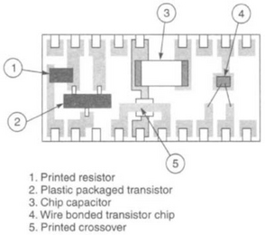
Hybrid microcircuits use patterns of thick and thin conducting films on an inert substrate to replace individual resistors, and to connect components such as capacitors, transistors and ICs into a complete circuit, thus saving both space and weight compared with PCBs. The first application of microcircuit techniques was for the wartime production of proximity fuses, using printed carbon composition resistors on ceramic substrates. The basic methods are recognisable 60 years later, even though modem materials have greatly improved performance.
Hybrid technology is always extending in new directions, as new components are being developed, which need novel packaging and interconnection techniques, for example;
For any electronics application, an appropriate construction can be selected which will meet the specification on performance, size and price.
Thick-film hybrids are most suitable for volume replication of relatively simple circuits, for example, the duplicated circuits in telephone exchanges. Screen printing is used to deposit patterns of conducting pastes on ceramic substrates, often at rates of thousands per machine per day. High-temperature firing fuses the pastes to the substrates, forming circuit elements of less than one-thousandth of an inch in thickness. Even so, these are still ‘thick’ films, compared with the film thickness of ‘thin’ film circuits. The process here is completely different, using photolithography and selective etching on purely metallic films to generate the circuits.
Microcircuits are discussed here in terms of materials and processes, and how they are applied to a range of circuit applications.
6.2.1 Thick-film materials
The materials used for hybrids are being continually up-graded and extended, to improve the final product. The basic properties of the materials are as follows.
The substrate material must be insulating, flat, non-reactive and thermally stable to the firing temperature (about 850°). The most widely used material is high purity (96%) alumina, used in plates from 50 × 50 mm (2 × 2 in.) to 175 × 125 mm (7 × 5 in.), and usually 0.63 mm (0.025 in.) in thickness, although any thickness between 0.25 and 2.5 mm (0.010-0.100 in.) can be obtained.


Exotic materials such as beryllia and aluminium nitride are occasionally used because of their better thermal conductivity in high power dissipation situations. Stainless steel, suitably insulated with glaze, is also used in power applications.
For any particular application, a conductor is chosen which will give adequate performance in terms of adhesion, solderability, etc., at an economic cost. The air-firing conductors are based on the precious metals silver, gold, palladium and platinum. The industry standard has been 3:1 Silver/Palladium, but demand for palladium for automobile catalytic converters has increased the cost greatly. Manufacturers now use conductors with ratios as low as 30:1, as well as replacing part of the palladium with platinum in a ternary alloy.
Copper and nickel systems have been developed because of the lower cost of the metal, but these conductors must be fired in a non-oxidising atmosphere (nitrogen, with oxygen < 20 ppm).
Modern resistor pastes are based upon ruthenium, either as the dioxide or as bismuth ruthenate. Resistivities between 1 Ω/sq and 10 MΩ/sq can be obtained, and intermediate values can be made by blending. The temperature coefficient of resistance (TCR) is ± 100 ppm or better, and load stability is good. Fired resistors are often overglazed with low-temperature glaze (550-600° C) which contributes to the mechanical and environmental protection of the resistors.
The circuit need not be limited to a single level on the substrate. Crossovers, using areas of dielectric glaze, enable conductors to cross one another, and if this is extended to cover the majority of the substrate, these circuits are known as ‘multilayers’. Multilayer hybrids are built up from layers of conductor tracks, separated by layers of dielectric glaze and interconnecting through windows (called vias) in the glaze. The glaze must tolerate multiple re-fires as each layer is added, and have a low dielectric constant, to minimise stray capacitance between tracks which cross. Resistors can be fired on top of glazes loaded with ceramic, giving results similar to resistors on alumina substrates.
Screen-printable protections are printed over trimmed resistors and cured at 200°C or less. Complete circuits can be dip-coated in liquid resin suspensions, powder coated, moulded or potted. The usual resin types which are used are silicones, epoxides or phenolics. Resins can be cured very quickly by U.V. lamps.
The components which can be attached to hybrids are of all shapes and sizes. The name ‘hybrid circuit’ is derived from the ability of this technology to mix all kinds of component to achieve the desired circuit characteristics.
Hybrids with only resistive, capacitive or inductive elements are called ‘passive’ hybrids. If semiconductor elements are included, they become ‘active’ hybrids. Miniature plastic-packaged semiconductor components are designed to be attached with solder, to pads on the hybrid. In this technique, known as ‘Surface Mount’, solder cream is printed over conductor pads on the substrate, into which the component feet are placed, prior to reflow. The solder cream consists of small solder balls, flux and solvent, and it is printed through a metal-foil stencil screen to give a suitable thickness of deposit.
Semiconductor chips are used in many packaging styles. Bare chips without any protective coating are wire bonded into circuits, and chips with moulded plastic protection are soldered. Complex chips are packaged in chip carriers, which are small hermetic packages, and permit the electrical parameters to be fully tested before soldering into a circuit.
The availability of active components for surface mounting led to the development of chip resistors which could be attached in the same way. Resistors are printed in a matrix on large ceramic substrates, which are divided into individual resistors. Solderable terminations at the ends are added by sputtering and plating. The immense market for mobile phones and the pressure to make them smaller has led to resistor chips as small as 0.5 × 0.25 mm (0.020 × 0.010 in.) which can be robotically placed. These tiny sizes are also popular because they use less ceramic and materials, hence they are more economical.
Chip capacitors consist of alternate layers of dielectric and conductor, sintered into a solid block, and with metallised terminations. The sizes range from 0.5 × 0.25 mm to 6 × 5.5mm (0.020 × 0.010 in. to 0.240 × 0.220 in.) and in value from 1 pF to 1 μF. High-value capacitors are miniaturised tantalum capacitors with metal end caps, or moulded with metal tabs.
Small wire-wound components such as inductors and transformers have also become available for hybrid use. A fibre-optic cable can be fed through the side wall of a hybrid package, for conversion of light information into an electrical output.
6.2.1.1 Thick-film processes
There are many stages between the customer’s original drawing and the final circuit.
The circuit elements are laid out using computer-aided design (CAD), from which photopositives are made with a photoplotter for each different ink to be printed on the substrate. The CAD will also prepare all the necessary drawings and instructions for production personnel. Typical conductor line width is 0.25-0.75 mm (0.010-0.030 in.) and resistors are usually not less than 1.25 mm (0.050 in.) square.
The photopositive is exposed and developed on a screen coated with U.V. sensitive emulsion. The screen mesh is stainless steel or synthetic fabric, with between 2.4 and 16 meshes/mm (60-400 meshes/in.). A thick film paste placed on the screen is printed onto the substrate by a moving flexible squeegee blade.
Printing machines can be loaded by hand, or fitted with mechanical feed systems, which take substrates from magazines, and transfer printed substrates to belt driers. The dried pastes are fired in multizone belt furnaces through a controlled temperature-time profile. A typical profile for conductors/resistors is 60 min through-time, with 10 min at a peak temperature of 850°C.
Resistors are trimmed by laser energy, which has the advantages of speed, precision and cleanliness. Substrates, printed with multiple circuits, are scribed using a more powerful laser, so the individual circuits can be snapped out.
Components attached by solder joints are placed on printed solder cream pads. To achieve the volume of work necessary, this is usually done by computer-controlled pick-and-place machines, which take each component from a separate reel, and place them in the correct position. There are several methods used to reflow the solder cream, which use heated belts, tunnel furnaces under nitrogen, and IR lamps, for example.
After soldering processes involving fluxes, the units may be cleaned, but many solder systems now are ‘non-clean’, because the flux is not a hazard to the operation of the circuit.
It is planned to cease using solders containing lead in electronics, for environmental reasons. There are several systems that could be used as alternatives, using tin alloyed with a variety of other metals. The greatest change affecting their use in hybrids is that the melting point is usually 30-40° C higher than the tin/lead eutectic, and the components have to withstand being heated to a higher temperature during assembly.
Semiconductor chips are usually glued into position with epoxy. This can be made conductive with silver or gold powder. Conductive epoxy is also used to attach capacitors to gold conductors, because solder dissolves gold very quickly. Bare chips are bonded with aluminium or gold wires of about 0.025 mm (0.001 in.) diameter. Aluminium wire is not used with pure gold conductors, because the bond strength deteriorates rapidly.
Hybrids may be mounted on their own terminals, or mounted inside a metal or ceramic package, which has its own terminals. The terminals are supplied on reels with perhaps 50 000 on a continuous strip. Insertion machines crop unwanted terminals and insert substrates into the strip, reeling up the strip afterwards. The strip is then fed through a continuous wave-soldering machine, then the soldered strip may be processed by a finishing machine, which crops each unit from the strip, tests it and packs it.
Metal packages are closed by soldering or welding a lid or cover to the header on which the substrate is mounted. A dry nitrogen atmosphere is maintained inside the package, to preserve the circuit from corrosion. The packages themselves are protected by plated films of tin, solder, nickel or gold.
6.2.2 Thin-film materials
The preferred substrate materials are glass or 99.6% alumina, because the surface finish has to be very smooth to allow the deposition of a uniform metal film. The film itself has a sheet resistivity between 50 and 500 Ω/sq with TCR ± 10 ppm, and many materials are in use, such as nichrome or tantalum nitride. The resistive film is overlaid by a conductive metal film. Conductors for wire bonding use gold, whereas if solderable conductors are required, nickel covered with a gold flash is used. To optimise conductor properties, there is a complex layered structure, with titanium and palladium layers under the gold to minimise diffusion effects, especially of chromium to the surface of the conductor.
Substrates can be metallised in-house, or bought-in with a film of known resistivity from an outside supplier. The add-on components are the same as for thick film.
6.2.2.1 Thin-film processes
Typically, the smallest resistor line width is 10 μm and conductor lines can be 50 μm. Designs can avoid cross-overs by wire-bonding over several lines, using the fine-line capability to crowd the conductor tracks. Designs cannot be photoplotted at this line width, so must be produced at a magnified scale, and reduced photographically. The photopositives are produced on glass because of the dimensional stability required.
A thin film of liquid photoresist is spun onto the surface of a substrate, and dried. The pattern is exposed and developed. Selective etchants remove the metal layers as required to produce the circuits.
Thin-film circuits produced in a matrix on glass substrates are separated by dicing with a diamond cutting wheel. Thereafter, individual circuits are assembled using the same methods as for thick film, although generally they are used in hermetic packages, which protect the glass substrates.
Thin film is less widely used than thick film for a number of reasons. The low resistor film resistivity means high value resistors take up too much area, the photomechanical process is not amenable to volume production, and the final package cost is high.
6.2.3 Types of hybrids, and their applications
With the wide range of materials and components available, the hybrid process can be used to produce any kind of circuit, from simple resistor networks to complex multilayers which can cost 1000 times the price of the simple unit. The following examples illustrate the capability of hybrids to produce circuits of increasing complexity.
6.2.3.1 Resistor networks
These networks are usually fabricated on ceramic substrates using thick film techniques, where the wide range of paste resistivities can be used to achieve any mix of resistor values. The package may be terminated by a single row of terminals along one edge (single-in-line SIL) or with two rows of terminals along 2 edges (dual-in-line DIL) with the substrate horizontal against the PCB. With a substrate thickness of 0.063 mm (0.025 in.), SIL circuits can be easily fitted to printed circuit boards on 2.5 mm (0.1 in.) pitches, and the height above the board can be between 3.75 mm (0.150 in.) and the maximum the customer will allow.
Design of a hybrid is very flexible, both in the size and shape of the substrate, and in the number and position of the terminals (the ‘pin-out’). Both sides of the substrate may be printed with resistors, provided the total dissipation does not exceed the substrate capability. If the network has to withstand power pulses from lightning surges, a thicker substrate may be used, which is stronger, and withstands the sudden heating effect. Many millions of these simple resistor networks are used in Telecoms, for example, as line feed resistors.
Divider networks made with the same resistor paste have good tracking performance, but to obtain the ultimate performance in this application, thin film is best.
6.2.3.2 Units with surface-mounted devices
It is a small step to convert a passive resistor network into an active circuit by incorporating semiconductor devices and capacitors. Every kind of component is available suitable for surface mounting. The components are assembled using pick-and-place machines, and reflow-soldered to the hybrid. The circuit may be protected by printed or dipped organic resin, or the circuit may be left in its overglazed state, since the add-on components have their own protection.
This is the most widely used type of circuit. It is used in Automotive applications for engine management systems and vehicle safety systems, and for general industrial applications.
6.2.3.3 Networks with wire-bonded chips
A substantial improvement in packing density can be realised by using bare chips, but the wire bonds must be protected, inside hermetic packages, or inside a globule of hard resin (‘globtop’)- Thick or thin film can be used, depending on the resistor values and tolerances required. The semiconductor dice are attached by conductive epoxy or eutectic bonding, then they are wire-bonded to the conductor pads. Manually, this can be a relatively slow operation, but automatic bonders are available with pattern recognition cameras, which can identify the bonding pads and make the bonds.
These circuits are used for military and aerospace applications-for radio and radar, sonar, ordinance fuses, electronic gauges for Head-up-displays. Other applications have been for proximity detectors, and control circuits for laser displays.
6.2.3.4 Power microcircuits
The hybrid process has been adapted to make motor drive circuits. These need very low conductor resistance, and the ability to bond 250 μm (0.010 in.) Al wire to the circuit and the power devices. These circuits use Direct-bonded Copper (DBC) substrates. Copper foil 300 μm (0.012 in.) in thickness is bonded directly to the alumina substrate, and the pattern is etched. The copper is given a nickel flash plate, then the components are attached and wire-bonded. The ceramic is then bonded to a heatsink, to prevent the semiconductors overheating.
6.2.3.5 Multilayers and multichip modules
The interconnect density of a hybrid can be multiplied several times by using multilayered conductors. It is possible to fit into a 30-pin package 40 × 25 mm (1.6 × 1 in.) about 15-20 integrated circuit (IC) chips, which would normally need a PCB at least 400 mm (4 in.) square. A high-conductivity conductor is used, which may be gold or silver.
A circuit can often be assembled from standard ‘building blocks’, which are already available as separate chips. Much time and expense may be saved, by making a hybrid to interconnect the separate chips, rather than designing a custom IC, with the necessary design and mask costs. This type of hybrid is known as a multichip module. One example made this way was an aircraft fuel status indicator.
6.2.3.6 LTCC modules (low temperature co-fired ceramic)
This is a multilayer, without the ceramic substrate. Dielectric is produced as a 250 μm (0.010 in.) ‘green tape’*TM, which is punched with vias, and printed with conductors. Circuit levels are made on separate sheets, which are stacked like a book, and fired at 850°C. The stack sinters into a solid block, containing all the interconnections, with excellent robustness and repeatable electrical characteristics. This technique is only viable for very large volume applications which can justify the tooling costs for punching the ceramic tape.
This manufacturing technique has been used in the ‘Bluetooth’ project. This is a system to allow any kind of computer-controlled device to link up with any other.
6.2.3.7 Microwave circuits
These circuits are made chiefly in thin film, because of the better control of line sizes and edge definition with this process, and the substrate material can be varied to exploit different dielectric constants.
6.2.3.8 Metal substrates
Although ceramic has admirable properties as a substrate, it is brittle, and the thermal conductivity is not as good as metals. Applications have arisen for heater elements, for example, in domestic kettles, which have been met by printing conductive elements on an insulating layer on a steel substrate. By careful matching of expansion coefficients, the element can withstand the thermal cycling, and in the case of the kettle elements, the rate of heat transfer is excellent.
The process is versatile; elements have been printed on tubes for electric showers, and on panels to prevent condensation in mobile phone base-stations, for example.
6.2.3.9 Standards
The appropriate UK Standard for hybrids is BS 9450, but this is now being replaced by a European standard in the form of EN 165000, which covers Capability and Qualification Approval. This incorporates best practice from UK, European and US standards. An additional standard EN 265000 is being produced for Technology Approval. The EN 165000 has been submitted for approval for conversion to an IEC standard.
Thick- and thin-film microcircuits
Colclaser, R.A. Microelectronics Processing and Device Design. Nottingham: Wiley; 1980.
Kittel, C. Introduction to Solid State Physics, 5th edition. New York: Wiley; 1986.
, Electronic Engineers Reference Book. Mazda, F., eds., 6th edition. New York: Butterworths, 1989. Chaps 28 to 31
Mckelvey, J.P. Solid State and Semiconductor Physics. London: Harper & Row; 1966.
Morgan, D.V., Board, K. Introduction to Semiconductor Microtechnology. New York: Wiley; 1983.
*TMDuPont trademark.