Voltage-Indicator/Monitor Circuits
The sources of the following circuits are contained in the Sources section, which begins on page 217. The figure number in the box of each circuit correlates to the source entry in the Sources section.
VOLTAGE-LEVEL INDICATOR

A tricolor LED, acts as the visual indicator of the voltage level. The voltage to be measured is connected to the two comparators in parallel. The first 20-kΩ trimmer defines a voltage between ± 5 V and this becomes the full-scale value of the reference voltage. The second trimmer is a fine adjustment to give any reference voltage between 0 V and the full-scale voltage. Thus, it is possible to select both positive and negative reference voltages. During the initialization procedure, a voltage, equal to the reference voltage of each comparator, is connected to the input terminal, and the offset-balance potentiometer is adjusted to give a reading between the high and low output voltage levels. The inverter following comp A ensures that, whatever the input voltage, at least one diode is lit. The two inverters following comp B leave the voltage largely unchanged, but provide the current necessary to illuminate the diode. The value of the resistance should be chosen so that the current through any single diode does not exceed the specified limit, usually 30 mA. The LED contains a red and a green diode with a common cathode. When both diodes are lit, a third color, orange, is emitted. With VrefA greater than VrefB, the output states given in the diagram apply.

FULL-SCALE FOUR-DECADE 3½-DIGIT DVM

This DVM circuit uses a National ADD3501 DVM chip and an LM336 reference IC to create a simple DVM with relatively few components. When making a single-range panel meter, the range-switching components can be left out, as required.
OVER/UNDER VOLTAGE MONITOR

Any potential from 1 to 15 V can be monitored with this circuit. Two lamps alert any undesirable variation. The voltage differential from lamp turn-on to turn-off is about 0.2 V at any setting. High and low set points are independent of each other. The SCRs used in the circuit should be the sensitive gate type. R3 must be experimentally determined for the particular series of SCRs used. This is done by adjusting R3 to the point where the undervoltage lamp turns on when no signal is present at the SCR2 gate. Any 15-V segment can be monitored by putting the zener diode, D1, in series with the positive input lead. The low set-point voltage will then be the zener voltage plus 0.8 V.
HIGH-INPUT RESISTANCE dc VOLTMETER
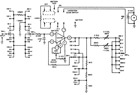
This voltmeter exploits a number of the CA3160 BiMOS op amp’s useful characteristics. The available voltage ranges from 10 mV to 300 V. Powered by a single 8.4-V mercury battery, this circuit, with zero input, consumes approximately 500 μA. Thus, at full-scale input, the total supply current will increase by 1000 μA.
dc VOLTMETER
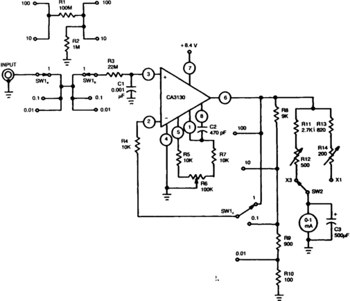
Fig. 21-6 Reprinted with permission of Radio-Electronics Magazine, November 1982. GE/RCA
This dc voltmeter, with high input resistance, uses a CA3130 BiMOS op amp and measures voltages from 10 mV to 300 V. Resistors R12 and R14 are used individually to calibrate the meter for full-scale deflection. Potentiometer R6 is used to null the op amp and meter on the 10-mV range by shorting the input terminals, then adjusting R6 for the first indication of upscale meter deflection.
VOLTAGE FREEZER
This circuit reads and stores voltages, thus freezing the meter reading even after the probes are removed. The op amp is configured as a unity-gain voltage follower, with C1 situated at the input to store the voltage. For better performance, use an LF13741 or a TL081 op amp in place of the 741. These two are JFET devices and offer a much higher input impedance than the 741.

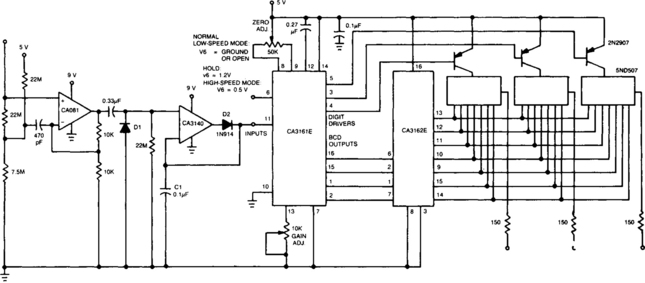
MULTIPLEXED COMMON-CATHODE LED-DISPLAY ADC

Here, a Teledyne TSC7135 DVM chip is used to drive a multiplexed 5-digit display. A CD4513BE CMOS IC, for common cathode drive, is used as a segment driver selected by pins 17 to 20 of the DVM chip. The transistors can be any suitable npn type, such as 2N3904, etc.
ac VOLTMETER
CA081 and CA3140 BiMOS op amp offer minimal loading on the circuits being measured. The wide bandwidth and high slew rate of the CA081 allow the meter to operate up to 0.5 MHz.
FET VOLTMETER I

A 2N3819 FET provides a solid-state VOM. The 2N3819 acts as a cathode follower in a VOM. The bias offset (meter null) obtained with R14 and R12 sets full-scale calibration. R2 through R9 should total about 10 MΩ. R10 is a protective resistor, and C2 provides ac bypassing to limit RF and noise pickup.
SENSITIVE RF VOLTMETER

This schematic shows a peak-reading diode voltmeter driven by two stages of amplification. A 100-μF capacitor provides a fairly large time constant, which results in satisfactory meter damping. The limited differential output voltage coupled with an overdamped meter prevents most needle pinning when you select an incorrect range position, or make other errors. An SPST toggle switch selects additional series resistance. This X2 function gives some more overlap of the sensitivity ranges. The resistance values shown are correct for use with a 100-μA meter with 1500-Ω internal resistance.
VOLTAGE MONITOR

If the battery voltage exceeds about 11 V, current flows through R1, D1, and R2. The voltage produced as a result of current flow through R2 is sufficient to bias transistor Q1 into conduction. That places the collector voltage of Q1 virtually at ground. Therefore, Q2, driven from the collector of Q1, is cut off, LED1 and current-limiting resistor R4 are connected in the collector circuit of Q2. With Q2 in the cut-off state, the LED does not light. Should Q1’s base voltage drop below approximately 0.6 V, Q1 turns off, biasing Q2 on, and illuminating LED1 to indicate that the battery voltage has fallen below the 11-V threshold level.
AUDIO MILLIVOLTMETER I

Capacitor C4 couples the output of U1 to a simple attenuator, which is used to provide a loss of 0 dB, 20 dB, or 40 dB, depending on the setting of range switch S1. The circuit’s sensitivity is 10-V rms for full-scale deflection, so the attenuator gives additional ranges of 100 mV and 1 V rms. The attenuator output is connected through capacitor C5 to common-emitter amplifier Q1, which has a high-voltage gain of 40 dB.
To get linear scaling on the meter, we have to use an active-rectifier circuit built around U2. That IC is connected so that its noninverting input is biased to the 0-V bus via R7. Capacitor C6 couples the output of Q1 to the noninverting input of U2; C7 is the compensation capacitor for U2.
The voltage gain of U2 is set by the difference in resistance between the output and the inverting input, and between the inverting input and the ground bus. One resistance is made up of the diode-bridge rectifier D1 through D4, the other by resistor R8. This circuit has a nearly flat frequency response to about 200 kHz.
AUDIO MILLIVOLTMETER II

This circuit has a flat response from 8 Hz to 50 kHz at −3 dB on the 10-mV range. The upper limit remains the same on the less sensitive ranges, but the lower frequency limit covers under 1 Hz.
LOW-VOLTAGE INDICATOR
Input terminal VIN is connected to the + V line of the circuit that the indicator is to monitor, and the grounds of both circuits are connected together. The position of potentiometer R1’s wiper determines Q1’s base voltage. As long as the transistor gets enough bias voltage to remain on, the low voltage at the collector will keep the SCR from firing. As the battery voltage starts to fall, the transistor’s base voltage will fall as well. When Q1 turns off (VINdrops), the collector voltage increases. That voltage provides enough gate drive to turn on the SCR, which turns on the LED. The LED could also be a buzzer or almost any other type of warning device.
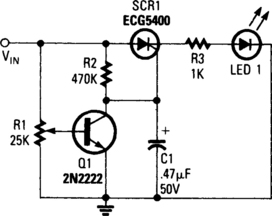
Fig. 21-15 Reprinted with permission of Radio-Electronics Magazine, January 1986. Copyright Gernsback Publications, Inc., 1986.
FET VOLTMETER II
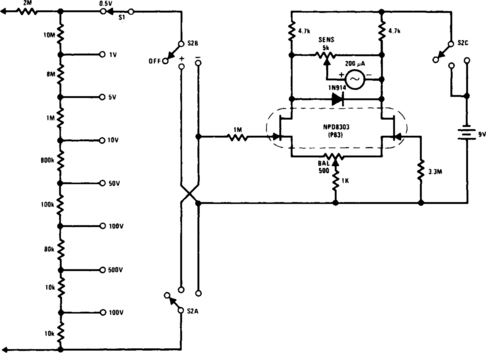
This FETVM replaces the function of the VTVM and rids the instrument of the usual line cord. In addition, FET drift rates are far superior to vacuum-tube circuits, allowing a 0.5-V full-scale range, which is impractical with most vacuum tubes. The low-leakage, low-noise NPD8303 is ideal for this application.
SIMPLIFIED VOLTAGE-LEVEL SENSOR
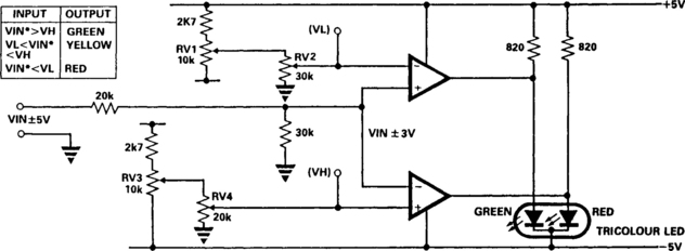
This circuit uses only one IC, either 1, LM393 dual comparator or ½, LM339 quad comparator. RV1 and RV3 set the full-scale reference voltage, and RV2 and RV4 set the switching thresholds to a value between 0 V and the full-scale reference. The change in input voltage needed to fully switch the output state is less than 0.05 mV (typical).
| INPUT | OUTPUT |
| VIN, VH | red |
| VH, VIN, VL | yellow |
| VIN, VL | green |
PEAK PROGRAM DETECTOR

This circuit will allow a multimeter to display the positive or negative peaks of an incoming signal. A 741, IC1, is used in the noninverting mode with R1 defining the input impedance. D1 or D2 will conduct on a positive or negative peak, charging C2 until the inverting input is at the same dc level as the incoming peak. This level will maintain the voltage until a higher peak is detected, then this will be stored by C2. Another 741, IC2, prevents loading by the multimeter. Connected in the noninverting mode as a unity-gain buffer, output impedance is less than 1 Ω. This circuit has a useful frequency response from 10 Hz to 100 kHz at ± 1 dB. High linearity is ensured by placing the diodes in the feedback loop of IC1, effectively compensating for the 0.6 V bias that these components require.
WIDE-RANGE ac VOLTMETER
In this circuit, a diode bridge is used as a meter rectifier. The offset voltage is compensated for by the op amp because the bridge is in the feedback network.

BIPOLAR REFERENCE SOURCE
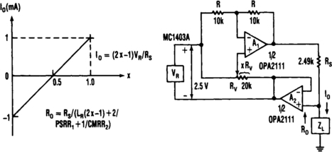
This current source has continuous control of the magnitude and polarity of its amplifier gain and needs only one voltage reference. The circuit includes reference VR, voltage-amplifier circuit A1 with gain-setting resistor RS, and bootstrap-follower amplifier A2. The bootstrapping converts the circuit to a current source and allows the load to be grounded. Any voltage developed across load ZL feeds back to the reference and voltage amplifier, making their functions immune to that voltage. Then, the current-source circuitry floats, instead of the load.
The voltage reference is connected to both the inverting and noninverting inputs of A1; this provides a balanced combination of positive and negative gain. The inverting connection has equal feedback resistors, R, for a gain of −1, and the noninverting connection varies according to the fractional setting, X, of potentiometer RV. X controls the noninverting gain and adjusting it counters the effect of some of the inverting gain. The value of X is the portion of RV’s resistance from the noninverting input of A1 to the temporarily grounded output of A2. Between potentiometer extremes, the current varies with X ±1 mA.
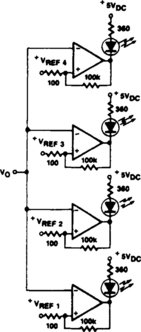
EXPANDED-SCALE ANALOG METER

The circuit consists of 0- to 1-mA meter M1, 6.2-V zener diode D1, and 12-kΩ, 1% resistor R1. R2 is included in the circuit as a load resistor for the zener diode. The value of R2 isn’t critical; use a value of 1000 to 1500 Ω. The meter reads from 6 to 18 V, which is perfect for checking a car’s charging system.