Current-Measuring Circuits
The sources of the following circuits are contained in the Sources section, which begins on page 217. The figure number in the box of each circuit correlates to the source entry in the Sources section.

This current meter ranges from 100 pA to 3 mA full scale. Voltage across input is 100 μV at lower ranges rising to 3 mV at 3 mA. The buffers on the op amp are to remove ambiguity with high-current overload. The output can also drive a DVM or a DPM.
ELECTROMETER AMPLIFIER WITH OVERLOAD PROTECTION

The preamplifier is protected from excessive input signals of either polarity by the 2N5909 junction field-effect transistor. A nulling circuit makes it possible to set the preamplifier output voltage to zero at a fixed low level (up to ± 10−8A) of the input current. This level is called the standing current and corresponds to the zero-signal level of the instrumentation. The opposing (offset) current is generated in the 109 feedback resistor to buck the standing current. Different current ranges are reached by feeding the preamplifier output to low-gain and high-gain amplifier chains. To reduce noise, each chain includes a 1.5-Hz corner active filter.
PICOAMMETER CIRCUIT
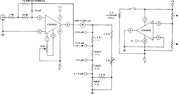
The circuit uses the exceptionally low input current (0.1 pA) of the CA3420 BiMOS op amp. With only a single 10-MΩ resistor, the circuit covers the range from ± 50 pA maximum to a full-scale sensitivity of ± 1.5 pA. Using an additional CA3420, a low-resistance center tap is obtained from a single 3-V lithium battery.
NANOAMPERE SENSING CIRCUIT WITH 100-MΩ INPUT IMPEDANCE

The circuit can be used as a sensitive current detector or as a voltage detector having high input impedance. R1 is set so that the voltage at point A is 0.5 to 0.75 V below the level that fires the 2N494C. A small input current (IIN) of only 40 nA will charge C2 and raise the voltage at the emitter to the firing level. When the 2N494C fires, both capacitors, C1 and C2, are discharged through the 27-Ω resistor, which generates a positive pulse with sufficient amplitude to trigger a controlled rectifier (SCR), or other pulse sensitive circuitry.
CURRENT MONITOR
R1 senses current flow of a power supply. The JFET is used as a buffer because ID = IS; therefore the output monitor voltage accurately reflects the power supply current flow.

GUARDED-INPUT PICOAMMETER CIRCUIT
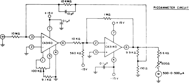
The circuit utilizes CA3160 and CA3140 BiMOS op amps to provide a full-scale meter deflection of ± 3 pA. The CA3140 serves as an X100 gain stage to provide the required plus and minus output swing for the meter and feedback network. Terminals 2 and 4 of the CA3160 are at ground potential, thus its input is operated in the “guarded mode.”
AMMETER WITH SIX-DECADE RANGE I

The ammeter measures currents from 100 pA to 100 μA without the use of expensive high-value resistors. Accuracy at 100 μA is limited by the offset voltage between Q1 and Q2 and, at 100 pA, by the inverting bias current of the LT1008.
AMMETER WITH SIX-DECADE RANGE II

The ammeter measures currents from 100 pA to 100 μA without the use of expensive high-value resistors. Accuracy at 100 μA is limited by the offset voltage between Q1 and Q2 and, at 100 pA, by the inverting bias current of the LT1008.
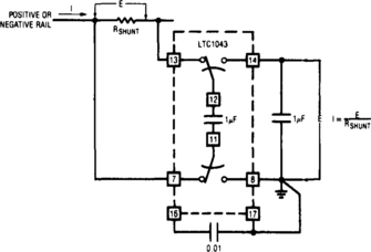
SUPPLY RAIL CURRENT SENSOR
The LTC1043 can sense current through a shunt in either of its supply rails. This capability has wide application in battery and solar-powered systems. If the ground-referred voltage output is unloaded by an amplifier, the shunt can operate with very little voltage drop across it, minimizing losses.
PICOAMMETER
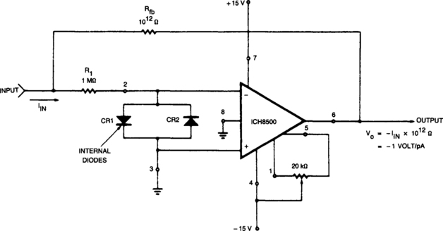
Care must be taken to eliminate any stray currents from flowing into the current summing node. This can be accomplished by forcing all points surrounding the input to the same potential as the input. In this case the potential of the input is at virtual ground, or 0 V. Therefore, the case of the device is grounded to intercept any stray leakage currents that may otherwise exist between the ±15-V input terminals and the inverting input summing junctions. Feedback capacitance should be kept to a minimum in order to maximize the response time of the circuit to step-function input currents. The time constant of the circuit is approximately the product of the feedback capacitance times the feedback resistor Rfb. For instance, the time constant of the circuit is 1 s if Cfb = 1 pF. Thus, it takes approximately 5 s (5 time constants) for the circuit to stabilize to within 1% of its final output voltage after a step function of input current has been applied. Cfb of less than 0.2 to 0.3 pF can be achieved with proper circuit layout.

