Probe Circuits
The sources of the following circuits are contained in the Sources section, which begins on page 217. The figure number in the box of each circuit correlates to the source entry in the Sources section.
DIGITAL LOGIC PROBE

The probe relies on the power supply of the CUT (circuit under test). The input to the probe, at probe tip, is fed along two paths. One path flows to the clock inputs of U2a and U2b. The other path feeds both the inverting input of U1c, which is set up as an inverting-mode integrator, and the noninverting input of U1b, which is configured as a noninverting unity-gain amplifier, in a logic-low state.
That low, below the reference set at pin 10, causes U1b’s output at pin 7 to become high. With Ub1 outputting low and U1c outputting high, LED1 is forward-biased, and lights. LED2, reverse-biased, remains dark. Suppose that the logic level on the same pin becomes high. That high is applied to pin 5 of U1b, causing its output to be high. LED2 is now forward-biased and lights, while LED1 is reverse-biased and becomes dark.
Assume that a clock frequency is sensed at the probe input; LED1 and LED2 alternately light, and depending on the frequency of the signal, can appear constantly lit. That frequency, which is also applied to the clock input of both flip-flops, causes the Q outputs of U2a and U2b to simultaneously alternate between high and low. Each time that the Q outputs of the two flip-flops decrease, the output of U1d increases, lighting LED3, indicating that a pulse stream has been detected.
650-MHz AMPLIFYING PRESCALER PROBE


The 650-MHz prescaler probe’s input is terminated by resistor R1 and is fed through C1 to the diode limiter (composed of D1 through D4). Those diodes are forward-biased by the +5-V supply for small-input signals and, in turn, they feed the signal to U1. However, for larger input signals, diodes D1 through D4 will start to turn off, passing less of the signal, and thus, attenuating it. But even in a full off state, the FH1100-type diodes will always pass a small part of the input to U1 because of capacitive leakage within the diodes. Integrated circuit U1, a Plessey SL952 bipolar amplifier, capable of 1-GHz operation, provides 20 to 30 dB of gain. The input signal is supplied to pin 10, U1 with the other input (pin 11) is bypassed to ground. The output signal is taken at pin 3 and pin 4, with pin 3 loaded by R4 and pin 4 by R5.
Integrated circuit 11C90, U2, is a high-speed prescaler that is capable of 650-MHz operation, configured for a divide-by-10 format. A reference voltage (internally generated) appears at pin 15 and is tied to pin 16, the clock input. This centers the capacitive-coupled input voltage from U1 around the switching threshold-voltage level. An ECL-to-TTL converter in U1 provides level conversion to drive TTL input counters by typing pin 13 low. Therefore, no external ECL-to-TTL converter is required at the pin 11 output. On the other hand, ECL outputs are available at U2, pin 8 (Q4) and at pin 9 (Q4), if desired. In that circuit configuration, pin 13 is left open, and U2 will use less power.
BATTERY-POWERED GROUND-NOISE PROBE

Oscilloscope measurements of ground noise can be unreliable because noise can enter your circuit via the scope’s three-pronged power plug. You can avoid this problem by using this ground-noise tester. Powered by two 9-V batteries, the circuit dissipates power only while push-to-test switch S1 is depressed. Noise pulses that reach IC2A’s switching threshold of about 1.5 to 1.8 V create a logic transition that triggers the monostable multivibrator (IC3), which stretches the pulse to produce a visible blink from LED D1. You set the noise reference level by adjusting threshold-adjust potentiometer R1, which lets the circuit respond to minimum pulse amplitudes ranging from about 0 to 1 V. For convenience, you can use a one-turn potentiometer for R1 and calibrate the dial by applying an adjustable dc voltage, monitored by an accurate voltmeter.
INJECTOR/TRACER
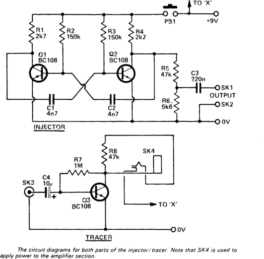
The unit has a separate amplifier and oscillator section, which allows them to be used separately, if need be. The injector is a multivibrator running at 1 kHz, with R5 and R6 dividing down the output to a suitable level (≈1 V). The tracer is a single-stage amplifier that drives the high-impedance earpiece. C4 decouples the input.
LOW-INPUT CAPACITANCE BUFFER
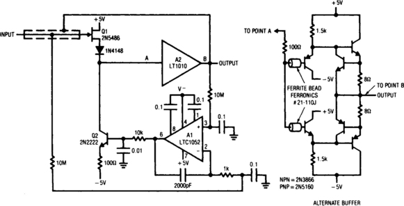
Q1 and Q2 constitute a simple, high-speed FET input buffer. Q1 functions as a source follower, with the Q2 current-source load setting the drain-source channel current. The LT1010 buffer provides output-drive capability for cables or for whatever load is required. The LTC1052 stabilizes the circuit by comparing the filtered circuit output to a similarly filtered version of the input signal. The amplified difference between these signals is used to set Q2’s bias, and hence Q1’s channel current. This forces Q1’s VGS to whatever voltage is required to match the circuit’s input and output potentials. The diode in Q1’s source line ensures that the gate never forward biases and the 2000-pF capacitor at A1 provides stable loop compensation. The RC network in A1’s output prevents it from seeing high-speed edges coupled through Q2’s collector-base junction. A2’s output is also fed back to the shield around Q1’s gate lead, bootstrapping the circuit’s effective input capacitance to less than 1 pF.
RF PROBE I

This RF probe is coupled with a fiber-optic cable to the test equipment. It utilizes inexpensive components to improve the probe performance at UHF frequencies. The receiving antenna in this probe feeds an envelope-detector diode. After amplification by the LF356 op amp, the low-frequency output modulates the LED, which in turn feeds the optical fiber. The design facilitates the use of a single battery for the op amp, with voltage splitting by means of the 1-kΩ potentiometer and the miniature 47-µF tantalum capacitors to provide decoupling. The gain control is easily adjusted to give the best dynamic range for a specific LED.
CMOS UNIVERSAL LOGIC PROBE

Only the CD4009AE hex buffer, two resistors, and two LEDs are required for a logic probe. CMOS logic probe features 1012Ω input impedance and covers the 3- to 15-V range. While LEDs are visible at all voltages, a 1-kΩ pot in place of R2 will allow the user to increase brightness at lower voltages.
4- TO 220-V TEST PROBE

Using inexpensive components, you can fit a simple probe circuit into a pencil-sized enclosure. When both LEDs are on, the probe indicates the presence of an ac voltage; either LED alone indicates the presence and polarity of a dc voltage. The diode-bridge arrangement allows one-way current source R1, R2, Q1, and Q2 to light either LED (or both) when the probe is activated by a test voltage. Diodes provide the necessary peak-inverse voltage rating; R3 and C1 provide a spike-suppression network to protect the current-source transistors.
FET PROBE
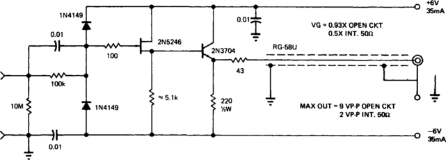
This FET probe has an input impedance of 10 MΩ shunted by 8 pF. Eliminating the protective diodes reduces the capacitance to about 4 pF. The frequency response of the probe extends from dc to 20 MHz (–1 dB), although higher frequency operation is possible through optimized construction and use of a UHF-type transistor. Zero dc offset at the output is achieved by selecting a combination of a 2N5246 and a source resistor, which yields a gate-source bias equal to the VBE of the 2N3704 at approximately 0 V. At medium frequencies, the probe can be used unterminated for near-unity gain; for optimum impedance converter probe high-frequency response, the cable must be terminated into 50 Ω. The voltage gain, when properly terminated, is precisely 0.5 X.
pH PROBE AND DETECTOR

The greatest sensitivity is achieved if R1 is approximately equal to the probe resistance. The circuit can be zeroed with R2, while the full-scale voltage is controlled by R5. The correlation between pH and output voltage might not be linear, which would necessitate a shaping circuit. A calibration scheme, using solutions of known pH, might be adequate and more reliable over a period of time because of probe variance.
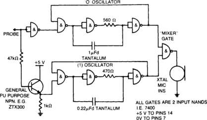
SIGNAL INJECTOR/TRACER

The injector is a CMOS oscillator with period approximately equal to 1.4 ×C1× R2 seconds. The values are given for 1-kHz operation. Resistors R3 and R4 divide the output to 1 V. Whereas the oscillator employs the gates in their digital mode, the tracer used them in a linear fashion by applying negative feedback from output to input. They are used in much the same way as op amps. The circuit uses positive ground. It offers an advantage at the earphone output because one side of the earphone must be connected to ground via the case. Use of a positive ground allows the phone to be driven by the two n-channel transistors inside the CD4001, which are arranged in parallel and are thus able to handle more current for better volume.
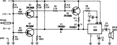
LOGIC PROBE
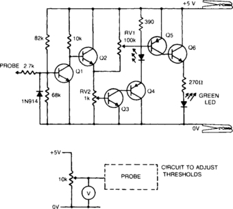
Transistors Q1 and Q2 form a buffer, providing the probe with a reasonable input impedance. Q3 and Q4 form a level detecting circuit. As the voltage across the base-emitter junction of the Q3 rises above 0.6 V, the transistor turns on, thus turning on Q4, and lighting the red (high) LED. Q5 and Q6 perform the same function, but for the green (low) LED. Q1, Q4, Q5 are all pnp general-purpose silicon transistors (BC178 etc). Q2, Q3, Q6 are all pnp general purpose silicon transistors (BC 108 etc.) The threshold low is ≤ 0.8 V, and the threshold high is ≤ 2.4 V.
LOGIC TEST PROBE WITH MEMORY
There are two switches: a memory disable switch and a pulse polarity switch. Memory disable is a pushbutton that resets the memory to the low state when it is depressed. Pulse polarity is a toggle switch that selects whether the probe responds to a high-level or pulse (+ 5 V) or a low-level or pulse (ground). Use IC logic of the same type as is being tested.

CLAMP-ON CURRENT-PROBE COMPENSATOR

A clamp-on “current probe,” such as the Tektronix P6021, is a useful means of displaying current waveforms on an oscilloscope. Unfortunately, the low-frequency response is somewhat limited, as shown in the table.
The more sensitive range on the P6021 is 2 mA/mV, but it has a roll-off of 6 dB per octave below 450 Hz. The compensator counteracts the low-frequency attenuation, and this is achieved by means of C3 and R4 + P1 in the feedback around op amp N1. The latter is a low-noise type, such as the LM725 shown; even so, it is necessary at some point to limit the increasing gain with decreasing frequency. Otherwise, amplifier noise and drift will overcome the signal. The values shown for C3R3 give a lower limit below 1 Hz. A test square wave of ± 10 mA is fed to the current probe so that P1 can be adjusted for minimum droop or overshoot in the output waveform. At high frequencies, the response begins to fall off at 100 kHz.
MICROVOLT PROBE

The current tracer helps locate a defective IC that is loading down the power supply. The tracer amplifies the small voltage drop caused by current flow along a fraction of an inch of PC wiring and drives an ordinary microammeter. Needle-point test probes are used to contact the edge of a PC trace and to follow the current to determine which branch the current takes. One-half of a dual 741 op amp forms a dc amplifier with ac feedback to prevent oscillations and hum-pickup problems. It drives a 50- to 100-μA meter. The other op amp provides a center tap for the 9-V battery supply and zero adjustment with R4. Two diodes protect the meter. Resistor R1 eliminates the necessity for shorting the probes when the meter is zeroed. The value of 1 Ω is large when compared with the resistance of the meter leads, plus the bridged portion of PC wiring.
CMOS LOGIC PROBE
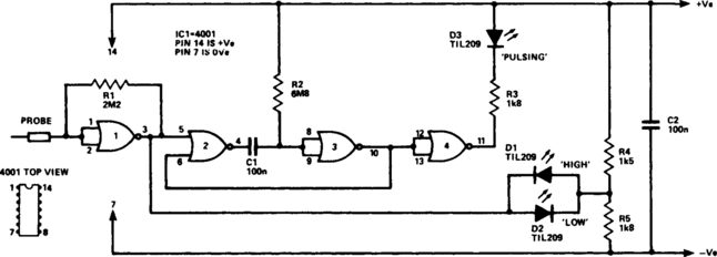
The logic probe can indicate four input states, as follows: floating input—all LEDs off; logic 0 input—D2 switched on (D3 will briefly flash on); logic 1 input—D1 switched on; pulsing input—D3 switched on, or pulsing in the case of a low-frequency input signal (one or both of the other indicators will switch on and show if one input state predominates).
RF PROBE FOR VOM

This probe makes possible relative measurements of RF voltages to 200 MHz on a 20,000 ohmsper-volt multimeter. RF voltage must not exceed the breakdown rating of the 1N4149 (approximately 100 V).
LOGIC PROBE
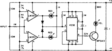
The probe indicates a high or low at 70% and 30% of V+ (5 to 12 V). One section of the voltage comparator (LM393) senses V in over 70% of supply and the second section senses V in under 30%. These two sections direct-drive the appropriate LEDs. The pulse detector is a CMOS one shot (MC14538), triggered on the rising edge of the LM393 outputs through 1N4148 diodes. With the RC values shown, it triggered reliably at greater than 30 kHz on both sine and square waves.
SIMPLE LOGIC PROBE

If the probe is connected to logic 0, Q1 will be turned on and light D1. At logic 1, Q2 will be turned on and light D2. For Q1 and Q2, any npn or pnp transistors will do. Also, D1 and D2 can be any LED.
AUDIO/RF SIGNAL-TRACER PROBE
This economical signal tracer is useful for servicing and aligning receivers and low-power transmitters. When switched to RF, the modulation on any signal is detected by the diode and amplified by the FET. Use twin-core shielded lead to connect the probe to an amplifier and to feed 6 V to it.

TTL LOGIC TESTER
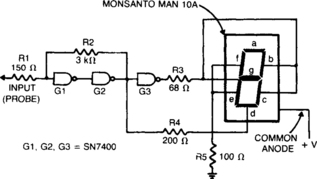
Gates G1 and G2 together with resistors R1 and R2 form a simple voltage monitor that has a trip point of 1.4 V. Gate G3 is simply an inverter. The display section of the tester consists of a common anode alphanumeric LED and current-limiting resistors. It indicates whether the input voltage is above or below 1.4 V, and displays an H or an L (for high or low logic-level) respectively.
1,000-MΩ dc PROBE
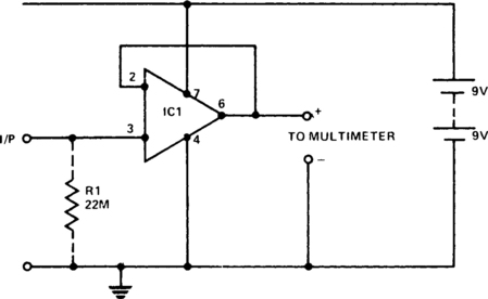
A 741 op amp is used with 100% ac and dc feedback to provide a typical input impedance of 1011 Ω and unity gain. To avoid hum and RF pickup, the input leads should be kept as short as possible and the circuit should be mounted in a small grounded case. Output leads can be long because the output impedance of the circuit is a fraction of an ohm. With no input the output level is indeterminate. Including R1 in the circuit though lowers the input impedance to 22 MΩ.
AUDIBLE TTL PROBE
When the probe is in contact with a TTL low (0) the probe emits a low note. With a TTL high (1), a high note is emitted. Power is supplied by the circuit under test.
LOGIC PROBE WITH THREE DISCRETE STATES

The circuit uses a dual LED. When power is applied to the probe through the power leads, and the input is touched to a low level or ground, Q1 is cut off. This will cause Q2 to conduct because the base is positive, with respect to the emitter. With Q1 cut off and Q2 conducting, the green diode of the dual LED will be forward biased, yielding a green output. Touching the probe tip to a high level will cause Q1 and Q2 to complement, and the red diode will be forward biased, yielding a red output from the LED. An alternating signal will cause alternating conduction of the red and green diodes and will yield an indication approximately amber. Thus, both static and dynamic signals can be traced with the logic probe.
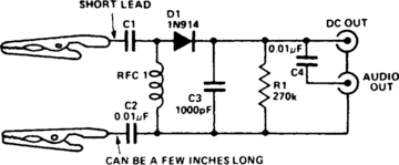
SINGLE INJECTOR-TRACER

This circuit will provide a nominal square-wave output in the audio range in the “Inject” mode; the harmonics of which should be heard at several MHz. In the “Trace” mode, the nonlinear operation of the amplifier will detect modulated RF signals, which will be filtered by the 0.001-µF capacitor and heard in the headphones.
GENERAL-PURPOSE RF DETECTOR
This circuit provides a dc output to a meter and an audio output (if necessary) for checking transmitters or modulated signals. It can be used also as a field-strength meter or transmitter monitor.
TONE PROBE (FOR TESTING DIGITAL ICs)
The tone probe uses sound to tell the status of the signal being probed. The probe’s input circuit senses the condition of the signal and produces either a low-pitched tone for low-level signals (less than 0.8 V) or a high-pitched tone for high-level signals (greater than 2 V).
RF PROBE II
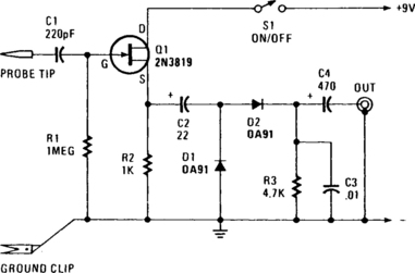
Transistor Q1, configured as a source-follower buffer stage, offering a bit under unity voltage gain, gives the unit a high-impedance input of about 1 MΩ shunted by about 10 pF, which puts only minimal loading on the equipment being tested. C1 serves as input dc blocking capacitor. The Q1 output is coupled by C2 to a simple AM detector circuit made up of D1, D2, R3 and C3. Capacitor C4 provides output dc blocking. Total current consumption should be somewhere around 1 mA. The circuit responds to frequencies from 100 kHz to well over 50 MHz.