Bridge Circuits
The sources of the following circuits are contained in the Sources section, which begins on page 217. The figure number in the box of each circuit correlates to the source entry in the Sources section.
BRIDGE CIRCUIT

The transistor is connected as an audio oscillator, using an audio transformer in the collector. The secondary goes to a linear pot. The ratio between the two parts of the pot from the slider is proportional to the values of Z1 and Z2 when no signal is heard in the phones.
TYPICAL TWO OP-AMP BRIDGE-TYPE DIFFERENTIAL AMPLIFIER

Using a CA3493 BiMOS op amp to provide high input impedance and good common-mode rejection ratio (depends primarily on matching of resistor networks).
BRIDGE TRANSDUCER AMPLIFIER
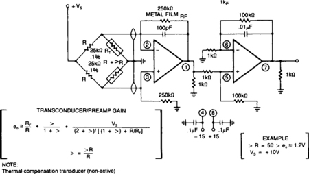
In applications involving strain gauges, accelerometers, and thermal sensors, a bridge transducer is often used. Frequently, the sensor elements are high resistance units requiring equally high bridge resistance for good sensitivity. This type of circuit then demands an amplifier with high input impedance, low bias current and low drift. The circuit shown represents a possible solution to these general requirements.
STRAIN GAUGE SIGNAL CONDITIONER WITH BRIDGE EXCITATION

The LT1007 is capable of providing excitation current directly to bias the 350-Ω bridge at 5 V. With only 5 V across the bridge, as opposed to the usual 10 V, total power dissipation and bridge warm-up drift is reduced. The bridge output signal is halved, but the LT1007 can amplify the reduced signal accurately.
BRIDGE BALANCE INDICATOR

The indicator provides an accurate comparison of two voltages by indicating their degree of balance (or imbalance). Detecting small variations near the null point is difficult with the basic Wheatstone bridge alone. Amplifying voltage differences near the null point will improve circuit accuracy and ease of use.
The 1N914 diodes in the feedback loop result in high sensitivity near the point of balance (R1/R2 = R3/R4). When the bridge is unbalanced the amplifier’s closed-loop gain is approximately RF/r, where r is the parallel equivalent of R1 and R3. The resulting gain equation is G = RF(1/R1 + 1/R3). During an unbalanced condition the voltage at point A is different from that at point B. This difference voltage (VAB), amplified by the gain factor G, appears as an output voltage, as the bridge approaches a balanced condition (R1/R2 = R3/R4), VAB approaches zero. As VAB approaches zero the 1N914 diodes in the feedback loop lose their forward bias and their resistance increases, causing the total feedback resistance to increase. This increases circuit gain and accuracy in detecting a balanced condition. The figure shows the effect of approaching balance on circuit gain. The visual indicator used at the output of the OP-07 could be a sensitive voltmeter or oscilloscope.
LOW-POWER COMMON-SOURCE AMPLIFIER

A circuit that will operate in the 10-to-20 μA range at a 12-V supply voltage. The diode protection is available in this configuration. The circuit voltage gain will be between 10 and 20, with extremely low power consumption (approximately 250 μW). This is very desirable for remote or battery operation, where minimum maintenance is important.

AUTO-ZEROING SCALE
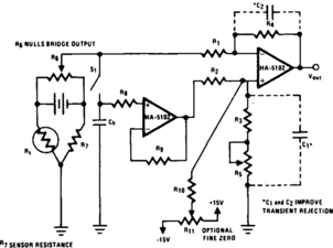
Electronic scales have come into wide use and the HA-510X, as a very low noise device, can improve such designs. This circuit uses a strain-gauge sensing element as part of a resistive Wienbridge. An auto-zero circuit is also used in this design by including a sample-and-hold-network.
The bridge signal drives the inverting input of a differentially configured HA-5102. The noninverting input is driven by the other half of the HA-5102 used as a buffer for the holding capacitor, CH. This second amplifier and its capacitor CH form the sampling circuit used for automatic output zeroing. The 20-kΩ resistor between the holding capacitor CH and the input terminal, reduces the drain from the bias currents. A second resistor RG is used in the feedback loop to balance the effect of R8. If R7 is approximately equal to the resistance of the strain gauge, the input signal from the bridge can be roughly nulled with R6. With very close matching of the ratio R4/ R1 to R3/R2, the output offset can be nulled by closing S1. This will charge CH and provide a 0-V difference to the inputs of the second amplifier, which results in a 0-V output. In this manner, the output of the strain gauge can be indirectly zeroed. R10 and potentiometer R11 provide an additional mechanism for fine tuning VOUT, but they can also increase offset voltage away from the zero point.
ACCURATE-NULL/VARIABLE-GAIN CIRCUIT
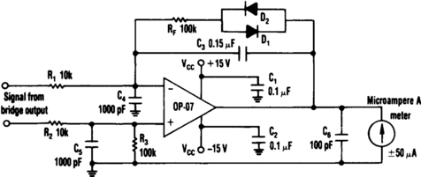
The circuit can use any general-purpose, low offset, low-drift op amp, such as the OP-07. The differential signal from the bridge feeds an amplifier that drives an ordinary, rugged ±50-μA meter. Near the null point, however, the drastically reduced signal level from the bridge requires very high gain to acheive a high null resolution. To provide the variable-gain feature, the op amp’s feedback path needs a dynamic resistance that increases as the input signal drops. Two common signal diodes, D1 and D2, in an antiparallel configuration in the feedback path supply function for all positive and negative inputs. To stabilize the op amp circuit at high gain, capacitors C3, C5, and C6 reduce response to high frequencies; capacitors C1 and C2 bypass the amplifier’s power supplies.
ac BRIDGE

The circuit provides a simple and cost-effective solution to matching resistors and capacitors. Impedances ZR and ZX form a half-bridge, while OSC and ![]() excite the bridge differentially. The external op amp is a FET input amplifier (LF356) with very low input bias current on the order of 30 pA (typical). C1 allows ac coupling by blocking the dc common-mode voltage from the bridge, while R1 biases the output of LF356 to 0 V at dc. Use of FET input op amp ensures that dc offset as a result of bias current through R1 is negligible. Ac output of the demodulator is filtered via the uncommitted amp to provide dc voltage for the meter. The 10-kΩ potentiometer, R5, limits the current into the meter to a safe level. Calibration begins by placing equal impedances at ZR and ZX, and the system offset is nulled by the offset adjust circuit so that Pin 1 is at 0 V. Next, known values are placed at ZX and the meter deviations are calibrated. The bridge is now ready to measure an unknown impedance at ZX with ±0.05% accuracy or better.
excite the bridge differentially. The external op amp is a FET input amplifier (LF356) with very low input bias current on the order of 30 pA (typical). C1 allows ac coupling by blocking the dc common-mode voltage from the bridge, while R1 biases the output of LF356 to 0 V at dc. Use of FET input op amp ensures that dc offset as a result of bias current through R1 is negligible. Ac output of the demodulator is filtered via the uncommitted amp to provide dc voltage for the meter. The 10-kΩ potentiometer, R5, limits the current into the meter to a safe level. Calibration begins by placing equal impedances at ZR and ZX, and the system offset is nulled by the offset adjust circuit so that Pin 1 is at 0 V. Next, known values are placed at ZX and the meter deviations are calibrated. The bridge is now ready to measure an unknown impedance at ZX with ±0.05% accuracy or better.
