
APPENDIX C
PROBLEM SOLUTIONS
Answers to all the odd-numbered problems are provided in this appendix.
Chapter 1
1. 25 = 32, 26 = 64, so 6 bits
3. 120 = 0x78 = 0b0111 1000
5. 0xF4 = 0b1111 0100
7. 0b1011 0111 = 0xB7 = 11*16 + 7 = 183
9. 0xB2 - 0x9F = 0x13. ~0x9F = ~(0b1001 1111) = 0b0110 0000 = 0x60. So 0xB2 - 0x9F = 0xB2 + ~0x9F + 0x01 = 0xB2 + 0x60 + 0x01 = 0x13
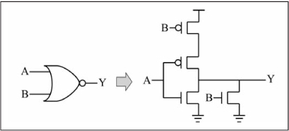
11. See Figure C.1.
15. 0.3 * period = 20 μs; so period = 20 μs/0.3 = 66.7 μs. Frequency = 1/(66.7 μs) = 15 kHz
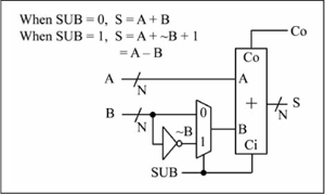
17. See Figure C.2.
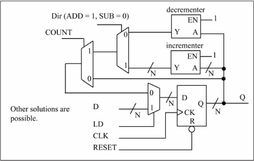
19. See Figure C.3.
Chapter 2
1. See Table C.1.
Table C.1: Problem 2.1 Solution
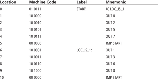
3. See Table C.2.
Table C.2: Problem 2.3 Solution

START: JC LOCAL
        OUT 1
        OUT X1
        OUT X2
        OUT X3
LOCAL: OUT Y1
       OUT Y2
       OUT Y3
       OUT Z1
       OUT Z2
       OUT Z3
       OUT Z4
       JMP START
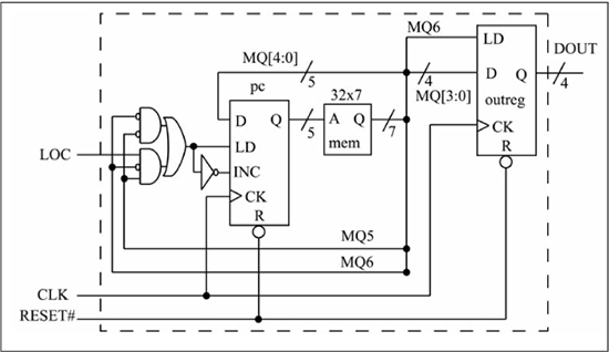
7. The first change is to increase the number of memory locations from 16 to 32. This causes the memory address bus to increase from 4 bits (24 = 16) to 5 bits (25 = 32). This means the Program Counter has to increase from 4 bits to 5 bits. Finally, the instruction size has to increase by one bit because the JC/JMP instruction data field specifies a location, which now requires 5 bits. So the new memory size is 32 × 7. See Figure C.4.
9. The opcode field must be increased from 2 bits to 3 bits; this changes the memory from a 16 × 6 memory to a 16 × 7 memory (each location now contains 7 bits).
Chapter 3
1. 0xBF900A
3. mov.w W8,W2
5. The immediate constant in this form of the add instruction is restricted to 5 bits (the range is 0 to 31). The immediate constant #35 does not fit in 5 bits.
7. W4
9. sub.w W3,W5,W6
11. 100 ns
13. One solution:
 mov  #32, W1            ; W1 = 32     this can be a word operation
 mov.b u8_j, WREG; WREG.LSB = u8_j
 mov.b W0, W2            ; W2.LSB =u8_j
 mov.b u8_i, WREG; W0.LSB =u8_i
 sub.b W0, W2, W0        ; W0.LSB = W0.LSB    W2.LSB = u8_i     u8_j
 sub.b W0, W1, W0        ; W0.LSB = W0.LSB    W1.LSB = (u8_i-u8_j) - 32
 mov.b WREG, u8_k; u8_k = W0.LSB = (u8_i    u8_j)    32
Another solution:
 mov.b u8_j, WREG; W0.LSB = u8_j
 sub.b u8_i, WREG; WREG.LSB = u8_i    WREG.LSB = u8_i    u8_j
 sub.b #32, W0           ; W0.LSB = W0.LSB    32 = (u8_i    u8_j) - 32
 mov.b WREG, u8_k; u8_k = W0.LSB = (u8_i    u8_j)    32
15. 12,500,000 (Instruction cycle frequency is 12.5 MHz)
17. W0=0x1038 (byte operation, only LSB of W0 changed)
19. Memory location 0x1004 = 0x2A19 (0x1005 = 0x2A, byte operation)
21. W3 = 0x1020
23. W0 = 0x4D18
25. WREG (LSB) = 0x2A + 0x06 = 0x30, so WREG = 0x1030
27. LSB of Memory location 0x1006 = 0x05 – 0x0A = 0xFB; so Memory Location 0x1006 = 0xE7FB
29. Memory location 0x1008 = 0xFFFE
31. Memory location 0x1008 = 0x0100 (0x1009 = 0x01)
Chapter 4
1. W0 = 0x0800, Z = 1, C = 1
3. W2 = 0x0002, Z = 0, C = 1
5. W1 = 0x0804, Z = 0, C = 1
7. W0 = 0xF8A6, Z = 0, C = 1
9. W4 = 0xFF5D, Z = 0, C = 1
11. W4 = 0x0000, Z = 0, C = 1 (status is not affected!)
13. W1 = 0xFFFF, Z = 0, C = 1
15. Location 0x1000 = 0x782A, Z = 0, C = 1
17. Location 0x1004 = 0x00FF, Z = 0, C = 1
19. Location 0x1004 = 0x7B0B, Z = 0, C = 1
21. Location 0x1002 = 0x0480, Z = 0, C = 1
23. W3 = 0x00F0, Z = 0, C = 1
25. W0 = 0x2000, Z = 0, C = 1
27. Location 0x1000 = 0x3854, Z = 0, C = 1
29. Location 0x1002 = 0xF701, Z = 0, C = 1
31. Location 0x1000 = 0x1C15, Z = 0, C = 1
33. Location 0x1002 = 0xFBC0, Z = 0, C = 0
35.
sl u16_j,WREG
        mov #0x30,W1
        sub W0,W1,W0
        add u16_i,WREG
        mov WREG,u16_k
37.
mov.b u8_p,WREG
ze W0,W1          ;W1 = (uint16) u8_p
sl u16_j,WREG     ;W0 = u16_j << 1
add W0,W1,W0      ;W0 = (uint16) u8_p +  ((uint16) u8_p)
mov #0x30,W1
sub W0,W1,W0      ;W0 = (uint16) u8_p +  ((uint16) u8_p) - 0x30
mov WREG,u16_k
       mov #0x400,W0
       cp  u16_k
       bra GEU, p39_if_body
       cp0.b u8_r
       bra NZ, p39_else_body
p39_if_body:
       nop    ;;if body
       bra    p39_end_if
p39_else_body:
       nop    ;; else body
p39_end_if:
41.
       mov #0x400,W0
       cp u16_k
       bra Z, p41_else_body
       mov.b u8_p,WREG
       cp.b  u8_r
       bra LEU,p41_else_body
p41_if_body:
       nop    ;;if body
       bra    p41_end_if
p41_else_body:
       nop    ;; else body
p41_end_if:
43.
p43_loop_top:
       mov u16_k,WREG
       cp u16_i
       bra Z,p43_loop_end
       nop   ;;loop body
       bra   p43_loop_top
p43_loop_end:
45.
p45_loop_top:
       nop    ;;loop_body
       cp0.b u8_r
       bra  NZ, p45_loop_top
       mov.b u8_q,WREG
       cp.b  u8_p
       bra LTU, p45_loop_top
p47:
     ;; Use W0 for u8_i
     clr.b u8_k       ;u8_k = 0
     clr.b W0       ;u8_i = 0
p47_loop_top:
     cp.b W0,#8      ;u8_i != 8
     bra  Z, p47_loop_exit
     btst.b u8_j, #0   ; test LSB of u8_j
     bra  Z, p47_skip
     inc.b u8_k       ;u8_k++
p47_skip:
     lsr.b  u8_j       ;u8_j = u8_j >> 1
     inc.b W0,W0       ;u8_i++;
p47_loop_exit:
Chapter 5
1.
p1_loop_top:
    mov u32_k,W0
    sub u32_i
    mov u32_k+2,W0
    subb u32_i+2       ;u32_i = u32_i    u32_k;
    mov u32_j,W0
    add u32_k,WREG
    mov W0,W2
    mov u32_j+2,W0
    addc u32_k+2,WREG
    mov W0,W3       ;W3:W2 = u32_j + u32_k
    mov u32_i,W0
    mov u32_i+2,W1  ;W1:W0 = u32_i
    cp W0,W2
    cpb W1,W3       ; u32_i < (u32_j + u32_k)
    bra LTU, p1_loop_top
3.
mov  u32_j,W0
ior  u32_i,WREG
mov  W0,u32_k
mov  u32_j+2,W0
ior  u32_i+2, WREG
mov  W0,u32_k+2
p5_loop_top:
     mov u64_k,W0
     sub u64_i
     mov u64_k+2,W0
     subb u64_i+2
     mov u64_k+4,W0
     subb u64_i+4
     mov u64_k+6,W0
     subb u64_i+6        ;u64_i = u64_i    u64_k;
     mov u64_j,W0
     add u64_k,WREG
     mov W0,W4
     mov u64_j+2,W0
     addc u64_k+2,WREG
     mov W0,W5
     mov u64_j+4,W0
     addc u64_k+4,WREG
     mov W0,W6
     mov u64_j+6,W0
     addc u64_k+6,WREG
     mov W0,W7           ;W7:W4 = u64_j + u64_k
     mov u64_i,W0
     mov u64_i+2,W1
     mov u64_i+4,W2
     mov u64_i+6,W3      ;W3:W0 = u64_i
     cp W0,W4
     cpb W1,W5
     cpb W2,W6
     cpb W3,W7           ; u64_i < (u64_j + u64_k)
     bra LTU, p5_loop_top
7.
p7:
     mov  u64_j,W0
     ior  u64_i,WREG
     mov  W0,u64_k
     mov  u64_j+2,W0
     ior  u64_i+2,WREG
     mov  W0,u64_k+2
     mov  u64_j+4,W0
     ior  u64_i+4,WREG

     mov  W0,u64_k+4
     mov  u64_j+6,W0
     ior  u64_i+6,WREG
     mov  W0,u64_k+6
     mov  W0,u64_k+4
     mov  u64_j+6,W0
     ior  u64_i+6,W0
     mov  W0,u64_k+6
9. 0xD6
11. –1117
13. 0xFF85
15. 0x90 – 0x8A = 0x06, Z = 0, N = 0, V = 0, C = 1
17. 0x2A – 0x81 = 0xA9, Z = 0, N = 1, V = 1, C = 0
19. These are signed numbers—i8_i = –96 and i8_j = +112—so comparison is false, assigning 8_k a value of 0.
21. 0xA0 >> 2 = 0xE8, assuming the sign bit is preserved.
23.
    mov i16_j, W0
    cp i16_k
    bra LT, p23_end_if      ; signed branch
    asr i16_i               ; preserve sign
    asr i16_i
p23_end_if:
25.
    mov.b i8_q, WREG
    se W0, W1            ; W1 = (int16_t) i8_q (sign extend)
    mov i16_k, W0        ; W0 = i16_k
    add W0, W1, W0       ; W0 = (i16_k + (int16_t) i8_q)
    asr W0, #2, W0       ; W0 = (i16_k + (int16_t) i8_q) >> 2
    mov #0xA34D, W1
    and W0, W1, W0       ; W0 = ((i16_k + (int8_t) i8_q) >> 2) & 0xA34D;
    mov WREG, i16_i
27. Code fragment:
    mov.b i8_q, WREG
    se    W0, W0         ; W0 = (int16_t) i8_q
    clr   W1
    btsc W0, #15
    setm W1              ; W1:W0 = (int32_t) i8_q
    asr  W1, W1
    rrc  W0, W0          ; W1:W0 = (int32_t) i8_q >> 1

    asr  W1, W1
    rrc  W0, W0          ; W1:W0 = (int32_t) i8_q >> 2
    mov.d W0, W2         ; W3:W2 = (int32_t) i8_q >> 2
    mov i32_s, W0
    mov i32_s + 2, W1    ; W1 = i32_s
    sub W0, W2, W0
    subb W1, W3, W1      ; W1:W0 = i32_s - (int32_t) i8_q >> 2
    mov #0x807F, W2
    mov #0x38DB, W3      ; W3:W2 = 0x38DB807F
    ior W0, W2, W0
    ior W1, W3, W1       ; W1:W0 = (i32_s - (int32_t) i8_q >> 2) | 0x38DB807F
    mov W0,i32_r
    mov W1,i32_r+2
29. 0x34FFDF
Chapter 6
1. See Table C.4.
3. W0 = 0x80FF, W1 = 0x0804
5. W0 = 0x0880, W1 = 0x0805
7. W0 = 0x0806, Memory Location 0x0804 = 0x8301
9. W0 = 0x0805, Memory Location 0x0804 = 0x8001
11. W2 = 0xCE46
13. W0 = 0x0806, Memory Location 0x804 = 0x7B03
15. W1=0x087B
17. Memory Location 0x0806 = 0x0603
19. W15 = 0x0806, Memory Location 0x0804 = 0x0806
21. W15 = 0x0802, W3 = 0xFB80
23. W15 = 0x080C, W14 = 0x0806, Memory Location 0x0804 = 0x0802
25. Return address = 0x020A + 4 = 0x020E
27.
; W0 = psz_1, W1 = psz_2, W2 used for u8_char
str_swap:
   cp0.b [W0]             ; *psz_1 != 0
   bra Z, str_swap_exit
   mov.b [W0], W2         ; u8_char = *psz_1

   mov.b [W1],[W0]        ; *psz_1 = *psz_2
   mov.b W2, [W1++]       ; *psz_2 = u8_char, psz_2++
   inc   W0, W0           ; psz_1++
   bra  str_swap
str_swap_exit:
   return
29.
; W0 = pi16_a, W1 = u8_cnt, W2 = i16_k
find_max:
    mov #0x8000, W2        ; i16_k = -32768
find_max_loop_top:
    cp0.b W1
    bra Z, find_max_exit
    cp W2, [W0]               ; i16_k < *pi16_a
    bra GE, find_max_skip  ;signed compare
    mov [W0], W2              ; i16_k = *pi16_a
find_max_skip:
    inc2 W0, W0               ; pi16_a++
    dec.b W1, W1              ; u8_cnt
    bra find_max_loop_top
find_max_exit:
    mov W2, W0                ; set up return value
    return ; W0 has pi16_a, W1 has u8_cnt, used W2 for i16_k
31.
putch:
    nop     ; dummy
    return
; W0 = psz_in
putstr:
    cp0.b [W0]
    bra Z, putstr_exit
    push W0             ; save W0 for subroutine call
    mov [W0], W0        ; get parameter for subroutine call
    call putch
    pop W0
    inc W0, W0          ; psz_in++
    bra putstr
putstr_exit:
    return
pu16_x            ; FP - 12
u8_i              ; FP - 10
u8_j              ; FP - 8
Rtn Addr (LSW)    ; FP - 6
Rtn Addr (MSW)    ; FP - 4
old FP            ; FP - 2
i16_k     ; <- New FP (+0)
free      ; <- New SP
35.
; use W0 = pu16_x, W1 = u8_i, W2 = u8_j
; W3 used for pu16_x + u8_i, W4 used for pu16_x + u8_j
; W5 used as offset registers
; local space used for i16_k
p35_u16_swap:
   lnk #2             ; allocate 2 words of space of i16_k
   mov #-12, W0
   mov [W14 + W5], W0       ; W0 = pu16_x
   mov #-10, W5
   mov.b [W14 + W5], W1     ; W1 = u8_i
   mov #-8, W5
   mov.b [W14 + W5], W2     ; W2 = u8_j
   ze W1, W1
   ze W2, W2                ; zero extend to 16 bits
   sl W1, W1
   sl W2, W2
   add W0, W1, W3    ; pu16_x+u8_i
   add W0, W2, W4    ; pu16_x+u8_j
   mov [W3], [W14]   ; u16_k = pu16_x[u8_i]
   mov [W4], [W3]    ; pu16_x[u8_i] = pu16_x[u8_j]
   mov [W4], [W3]    ; pu16_x[u8_j] = u16_k;
   ulnk
   return
37.
  .bss                     ;uninitialized data section
; These start at location 0x1000 because 0-0x0FFF reserved for SFRs
au16_values: .space 2*6    ; data memory space
.text
   mov #__SP_init, W15     ;Initialize the stack pointer
   mov #__SPLIM_init, W0
   mov W0, SPLIM           ;Initialize the stack limit register

   call p37_init_variables
   call p37_main
   reset

ui16_swap:
   nop
   return

p37_main:

   mov #au16_values, W0
   mov #3, W1
   mov #4, W2
   call ui16_swap
p37_done: bra p37_done


au16_values_const:  .word 489, 45, 1000, 238, 30000, 10134

p37_init_variables:
    mov #psvpage(au16_values_const), DSRPAG    ; enable PSV
; copy au16_values_const to au16_values
    mov  #psvoffset(au16_values_const), W2
    mov  #au16_values, W3                      ;destination address in data memory
    mov  #((6*2)-1), W4                        ;(number of bytes)-1 to copy
    call p37_byte_copy
    return

p37_byte_copy:
    repeat W4
    mov.b [W2++], [W3++]
    return
Chapter 7
1. W9:W8 = 0x0009 FF88
3. W9:W8 = 0x0009 FF88
5. W9:W8 = 0xFFFF F448
7. W9:W8 = 0x000B F448
9. W0 = 0x1015, W1 = 0x0003
11. W0 = 0x3329, W1 = 0x0003
13. W0 = 0x00AB, W1 = 0x0010, overflow
15. W0 = 0xFFF2, W1 = 0x00FF
17. W0 = 0x3F01, W1 = 0x0000
19. 0xC4 = 196, 196/256 = 0.765625
21. 0xC4 = –60, –60/128 = –0.46875
23. 23.33 × 8 = 186.64, 186 = 0xBA
25. –0.2325 × 128 = –29.76, –29 = 0xE3
27. 0x7F (+127)
29. 0xFF (255)
31. –0.15625 = 0xBE200000
33. 0x42F18000 = 120.75
35. Comparing a and b, where a and b are single precision floating-point numbers. Return 1 if
a > b, –1 a <b, and 0 if a == b.
if (sign(a) != (sign(b)) {
    if (sign(a)) return   1;
    else return 1
}
// signs are equal, check exponent fields
if (exponent(a) != (exponent(b)) {
    if (exponent(a) < exponent(b)) return   1;
    else return 1
}
// signs and exponents are equal
if (significand(a) != (significand(a)) {
    if (significand(a) < significand(b)) return   1;
    else return 1
}
return 0;   // the numbers are equal.
37. 99 – 58 + 1 = 42
Chapter 8
1. _TRISB5 = 1 (input), _CNPUB5 = 0 (pull-up disabled), and _ODCB5 = 0 (open-drain disabled). This is a digital-only pin.
3. _TRISB2 = 1 (input), _ANSB2 = 1 (analog disabled), _CNPUB2 = 1 (pull-up enabled), and _ODCB2 = 0 (open-drain disabled). This is an analog/digital pin.
5. CONFIG_RB5_AS_DIG_INPUT(); // Pull-ups and open drain disabled by default.
7. Current (Doze/4) = (42.3 – 17.6)/4 + 17.6 = 23.8 mA
9. The string “Howdy Y’all!” is printed, and the WDT is enabled by _SWDTEN = 1. The code enters the infinite wait while (1) loop; the WDT expires causing the processor to reset. After reset, main() is re-entered and the process is repeated.
11. The string “Howdy Y’all!” is printed and then the CPU enters sleep mode (asm(“pwrsav #0”)) and stays there; nothing else appears on the screen.
13. Uses the same ASM chart as Figure 8.28, except “Toggle LED1” on exit of WAIT_FOR_RELEASE is replaced by “Toggle u8_blinkFlag”, where u8_blinkFlag is a variable in the while (1) loop that controls blinking of the LED.
int main(void) {
  STATE e_mystate;
  uint8_t u8_blinkFlag;
  configBasic(HELLO_MSG);
  CONFIG_SW1(); CONFIG_LED1();
  e_mystate = STATE_WAIT_FOR_PRESS;
  u8_blinkFlag = 1;
  LED1 = 0;
  while (1) {
    if (u8_blinkFlag) {
      LED1 = !LED1;
      DELAY_MS(100);   //blink
    }
    switch (e_mystate) {
      case STATE_WAIT_FOR_PRESS :
         if (SW1_PRESSED()) e_mystate = STATE_WAIT_FOR_RELEASE;
        break;
      case STATE_WAIT_FOR_RELEASE :
        if (SW1_RELEASED()) {
           e_mystate = STATE_WAIT_FOR_PRESS;
           u8_blinkFlag = !u8_blinkFlag;  // toggle blink flag
        }
        break;
     default:
        e_mystate = STATE_WAIT_FOR_PRESS;
    }//end switch(e_mystate)
    DELAY_MS(DEBOUNCE_DLY);      // Debounce
    doHeartbeat();     // Show that we are alive
    }//end while
}//end main
15. Uses the same ASM state transition as Figure 8.28. On exit from each state, there is a function call to changeLEDs() that changes the LED states.
void changeLEDs(void) {
  if (!LED1 && !LED2) {
     LED2 = 1;
     return;
  }
  if (!LED1 && LED2) {
     LED1 = 1; LED2 = 0;
     return;
  }
  if (LED1 && !LED2) {
     LED2 = 1;
     return;
  }
  if (LED1 && LED2) {
     LED1 = 0; LED2 = 0;
     return;
  }
}

int main(void) {
  STATE e_mystate;
  configBasic(HELLO_MSG);
  CONFIG_SW1(); CONFIG_LED1(); CONFIG_LED2();
  e_mystate = STATE_WAIT_FOR_PRESS;
  LED1 = 0; LED2 = 0; // LEDs are off.
  while (1) {
    switch (e_mystate) {
      case STATE_WAIT_FOR_PRESS :
         if (SW1_PRESSED()) {
            e_mystate = STATE_WAIT_FOR_RELEASE;
            changeLEDs();  // change the LED states
         }
        break;
      case STATE_WAIT_FOR_RELEASE :
        if (SW1_RELEASED()) {
           e_mystate = STATE_WAIT_FOR_PRESS;
           changeLEDs();  // Change the LED states
        }
        break;
     default:

        e_mystate = STATE_WAIT_FOR_PRESS;
    }//end switch(e_mystate)
    DELAY_MS(DEBOUNCE_DLY);    // Debounce
    doHeartbeat();      // Show that we are alive
  }//end while
}//end main
17.
//written in a simple style
uint8_t testDFFAsync(uint8_t u8_op) {
  DFF_R = 1; DFF_S = 1;  // negate
  DELAY_US(1);
  if (u8_op) {
   //reset
   DFF_R = 0;  // assert
   DELAY_US(1);
   DFF_R = 1;   // negate
   DELAY_US(1);
   if (DFF_Q) return 0;  // incorrect output
   else return 1; // correct output
  } else {
     // set
   DFF_S = 0;  // assert
   DELAY_US(1);
   DFF_S =1;   // negate
   DELAY_US(1);
   if (DFF_Q) return 1;  // correct output
   else return 0; // incorrect output
  }
}
19.
//written in a simple style
uint8_t testGate(void) {
  GATE_A = 0; GATE_B = 0;
  DELAY_US(1);
  if (!GATE_Y) return 0;
  GATE_A = 0; GATE_B = 1;
  DELAY_US(1);
  if (!GATE_Y) return 0;
  GATE_A = 1; GATE_B = 0;
  DELAY_US(1);

  if (!GATE_Y) return 0;
  GATE_A = 1; GATE_B = 1;
  DELAY_US(1);
  if (GATE_Y) return 0;
  return 1;
}
Chapter 9
1.
int main(void) {
  volatile uint16_t u16_val;
  uint8_t* pu8_1;
  uint16_t* pu16_1;

  configBasic(HELLO_MSG);
  /** start **/
  pu8_1 = (uint8_t *) &u16_val; // will be an even address
  pu8_1++;                  // advance to odd address
  pu16_1 = (uint16_t *) pu8_1;  // assign to integer pointer
  while (1) {
    outString(“Hit a key to start address error trap...”);
    inChar();
    outString(“OK. Generating the address error trap (Vector number = 2).
”
               “The trap is not handled, so
”
               “the _DefaultInterrupt handler should be
”
               “called, causing the chip to reset.

”);
    u16_val = *pu16_1;  //generates the trap, word access to odd address
    doHeartbeat();
  }// end while (1)
}
3. What happens is not obvious. You may think in looking at Figure 9.10 that the RB2 low pulse width is reduced after the NOPs are removed. However, what actually happens is that the low pulse width is increased. This is because the CNIF flag is cleared before the change in RB2 status has propagated through the change notification logic, and the CNIF flag is set during the two cycles of the ISR return. This means the main() code is not executed. When the CNIF flag is cleared on the second execution of the ISR, it remains cleared and the main() code is re-entered.
5. _CNIEA2
_CNIEA4 = 1;     // RA4 CN, or use ENABLE_RA4_CN_INTERRUPT()
_CNIEB12 = 1;    // RB12 CN, or use ENABLE_RB12_CN_INTERRUPT()
_CNIF = 0;       // clear the flag
_CNIE = 1;       // enable the interrupt
_CNIP = 1;       // choose a priority higher than 0
9. One time; on press the CNIF flag is set and the _CNInterrupt() ISR is executed, disabling the CN interrupt on RB12 and clearing the CNIF flag. On release the CNIF flag is set, but the interrupt is not recognized since it is disabled.
11. The _CNInterrupt() ISR is not executed because the change notification priority is 0; it must be greater than 0 for the ISR to be executed.
13. A, B, C, and D. Both interrupts are enabled, with negative edge, and both have the same priority. The INT0 ISR is executed first on the simultaneous interrupt on the press because it comes first in the vector table of Figure 9.3 (it has a higher natural priority).
15. C, D, A, and B. Both interrupts are enabled. Both have the same priority. INT0 is positive edge triggered and INT1 is negative edge triggered. INT1 ISR is executed first on the press, and then INT0 on the release.
17. A and B. Only INT0 interrupt is enabled (the INT1 interrupt enable bit is 0, which disables this interrupt).
19. A, B, C, C, C, ... (infinite loop). Both interrupts are enabled, with negative edge, and both have the same priority. The INT0 ISR is executed first on the simultaneous interrupt on the press because it comes first in the vector table of Figure 9.3 (it has a higher natural priority). The changes mean that the INT1 interrupt remains enabled, and the interrupt flag is not cleared, so the INT1 ISR becomes stuck in an infinite loop.
21. Ticks = Time × FCY/Pre = 1.2 ms × 30 MHz/8 = 4,500. To generate a periodic interrupt with this period, a value of 4,500 – 1 = 4,499 would be written to the timer period register.
23. Time = Ticks × Pre/FCY = 65,536 × 8/10 MHz = 0.05243 s = 52 ms. Note that the largest value that can be written to PR2 is 0xFFFF = 65,535 and the timeout period is PR2 + 1, so 65,535 + 1 = 65,536 = 216.
25. Uses the same ASM state transition as Figure 8.28. On exit from each state, there is a function call to changeLEDs(), which changes the LED states. A periodic interrupt is used to sample the switch inputs. The configTimer3() function is the same as used in Figure 9.20. The following code lists functions and variables changed in chap09ledsw_ch_revised.c. The remainder of the file is unchanged but necessary for the program to run.
typedef enum  {
  STATE_PRESSED,
  STATE_RELEASED,
} state_t;

const char* apsz_state_names[] = {
  “STATE_PRESSED”,
  “STATE_RELEASED”,
};

void changeLEDs() {
  if (!LED1 && !LED2) {
     LED2 = 1;
     return;
  }
  if (!LED1 && LED2) {
     LED1 = 1; LED2 = 0;
     return;
  }
  if (LED1 && !LED2) {
     LED2 = 1;
     return;
  }
  if (LED1 && LED2) {
     LED1 = 0; LED2 = 0;
     return;
  }
}

void update_state(void) {
  static state_t e_state = STATE_RELEASED;

  switch (e_state) {
    case STATE_RELEASED:
      if (PB_PRESSED()) {
        e_state = STATE_PRESSED;
        changeLEDs();
      }
      break;

    case STATE_PRESSED:
      if (PB_RELEASED()) {
        changeLEDs();
      }
      break;

    default:
      ASSERT(0);
  }

  print_state(e_state);
}
27. Uses the same ASM state transition as Figure 8.23. The following code lists functions and variables changed in chap09ledsw_ch_revised.c. The remainder of the file is unchanged but necessary for the program to run. typedef enum {
typedef enum  {
  STATE_PRESSED,
  STATE_RELEASED,
} state_t;

const char* apsz_state_names[] = {
  “STATE_PRESSED”,
  “STATE_RELEASED”,
};

void update_state(void) {
  static state_t e_state = STATE_RELEASED;
  static uint16_t u16_isBlinking = 0;

  switch (e_state) {
    case STATE_RELEASED:
      // Blink the LED by scheduling the timer to call this again.
      // Only do this if we aren’t interrupted by a pushbutton press, during
      // which _CNIE = 0.
if (_CNIE) {
        timer3_arm(250);
        LED1 = !LED1;
      }
      if (PB_PRESSED()) {
        e_state = STATE_PRESSED;
      }
      break;

    case STATE_PRESSED:
      if (PB_RELEASED()) {
        isBlinking = !isBlinking; // Toggle blinking
      }
      break;

    default:
      ASSERT(0);
  }
  print_state(e_state);
}
Chapter 10
1. 32 wires transfer 4 bytes; a data transfer every second rising clock edge with an 8 MHz clock gives 4 million transfers per second, so 16 million bytes per second (16 MB/s).
3. 1/19,200 = 52.1 μs
5. Transfer time for one byte is 1 byte × (8 data + 1 start + 1 stop) × 1/115,200 = 10 / 115,200 = 1/11,520 s. Bytes transferred in one second: 1 s / (1/11,520 s) = 11,520 bytes. Bandwidth in bytes/sec is then 11,520 B/s.
7. See Figure C.5.

9. 0x38 = 0b0111000 has an odd number of ones, so parity bit = 1 to make an even number of 1 bits for even parity.
11. The UART receiver can hold 4 bytes in the FIFO and 1 byte in the shift register for a total of 5 bytes. Time before overrun is then 5 bytes × (8 data + 1 start + 1 stop) × 1/38,400 = 0.001302 s. The time for one instruction is 1/40 MHz = 25 ns. The number of instructions is then 0.001302 s/25 ns = 52,080.
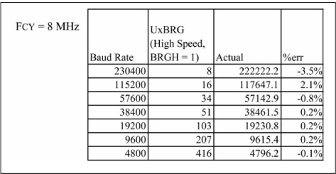
13. From Figure C.6 only baud rate 230,400 is not supported.
15. The primary difference is that the RS-232 standard uses single-ended signaling while RS-422 uses differential signaling, which allows it to reject common-mode noise.
19. CKP = 0, CKE = 1
21. Writing the value 0xC0 returns wiper W0A contents, while writing the value 0xC2 returns wiper W1A contents.
23. The minimum period is 100 ns, so 10 MHz.
25. CKP = 0, CKE = 1
27. 64 bytes
29. 256 taps
31. When the ADD_SEL pin is low, this sets the slave address as 0xA2.
//using primitive functions from 10.44(a)
startI2C1();
putI2C1(0xA2);
putI2C1(0x03);               // select resistor 1
rstartI2C1();                // repeated start
putI2C1(0xA3);               // address byte, read operation
u8_potVal = getI2C1(1);      // read the wiper register
stopI2C1();

//using transaction functions from 10.44(b)
write1I2C1(0xA2, 0x02);
read1I2C1(0xA2, &u8_potVal);   //read function sets LSb of address
33. The total capacity is 8,192 bits organized as 1024 x 8.
35. 8 bytes
37. 31.5 ms
39. To determine write time, first do a page write. Then set a PIO pin high and start polling for the end of write. Once the write is finished, set the PIO pin low. The measured pulse width is the write time. Experimental results for the 24LC515 at 3.3 V give typical write times of 3.1 ms; this time is not dependent on the number of bytes written in the page.
41.
uint8_t u8_configReg;
 write1I2C1(0x90, 0x51);    //in one-shot mode, 0x51 starts a conversion.
//poll for end of conversion
do {
  read1I2C1(0x90, 0xAC, & u8_configReg);   //configuration registers
}
while (u8_configReg & 0x80)  //check DONE bit
Chapter 11
1. 12 bits, since 211 = 2,048 and 212 = 4,096, so you need at least 12 bits.
3. 80 minutes × 60 = 4,800 seconds, and 16 bits = 2 bytes. Each track is 2 bytes × 44.1 × 103 × 4,800 = 423,360,000 bytes for each track. Two tracks = 2 × 423,360,000 = 846, 720, 000 bytes.
5. Each color (red, green, and blue) has 28 combinations, so 28 × 28 × 28 = 224 ~ 16.8 million (16,777,216).
7. Step 1: Guess is 1000, so Vref = 8/16 × 4 V = 2 V. Vin of 1.8 V < 2 V, so D[3] = 0.
Step 2: Guess is 0100, so Vref = 4/16 × 4 V = 1 V. Vin of 1.8 V > 1 V, so D[2] = 1.
Step 3: Guess is 0110, so Vref = 6/16 × 4 V = 1.5 V. Vin of 1.8 V > 1.5 V, so D[1] = 1.
Step 4: Guess is 0111, so Vref = 7/16 × 4 V = 1.75 V. Vin of 1.8 V > 1.75 V, so D[0] = 1.
The final 4-bit conversion returns 0111.
9. The reference voltages for the seven comparators from the resistor string are 7/8×VREF, 6/8×VREF, 5/8×VREF, 4/8×VREF, 3/8×VREF, 2/8×VREF, and 1/8×VREF. The input voltage of 2.7 V is between 6/8×VREF = 3.0 V and 5/8×VREF = 2.5 V, so the comparators’ outputs are 0011111.
11. 10 bits of resolution is specified, so:
1 LSb = 3.0 V/210 = 3.0 V/1024 = 0.00293 V = 2.93 mV.
0.1% × 3.0 V = 0.003 V, so 3 mV/2.93 mV × 100% = 102.4% of a LSb.
This means that only 9 bits of the PIC24 ADC 10-bit result should be used, as the voltage reference is not accurate enough for 10 bits.
13. 0.449 V / 3.3 V × 1024 = 139.3, truncate and convert to hex = 0x08B. 2.91 V/3.3 V × 1024 = 902.98, truncate and convert to hex = 0x386.
15. 0x7F = 127; 127/256 × 3.3 V = 1.637 V; 0x4B = 75; 75/256 × 3.3 V = 0.967 V; 0xCB = 203; 203/256 × 3.3 V = 2.617 V.
17. 0x17F = 383; 383/4,096 × 3.0 V = 0.280 V; 0x74B = 1,867; 1,867/4,096 × 3.0 V = 1.367 V; 0xCCB = 3,275; 3,275/4,096 × 3.0 V = 2.398 V.
19. The LM60 outputs 6.25 mV for every 1°C and has a DC offset of 424 mV, so a 10-bit ADC stepsize with a 3.3V reference of 3.222 mV is equivalent to 0.5155°C. 12-bit ADC stepsizes with a 3.3V reference are 0.8057 mV that is equivalent to 0.1290°C, which is 1/4 of the previous answer.
21. A precision of 1.5 °C corresponds to a voltage of (1.5 × 6.25 mV) = 9.375 mV. 3.3V/9.375 mV = 352 steps. Therefore, the ADC must have at least 9 bits.
Chapter 12
1. TDelta = (1 - 1) × (0xFFFF + 1) + (0x0000 - 0xA000) + 0x1200 = 0 + 0x6000 + 0x1200 = 24576 + 4608 = 29184 ticks. 1 Tick = 1/40 MHz × 8 = 200 ns = 0.2 μs, so 29184 ticks × 0.2 μs = 5836.8 μs.
3. 232 ticks × 1/40 MHz × 8 = 4294967296 × 1/40 MHz × 8 = 6871.9 s = 6872 s.
5. Time = 2,000 ticks × 1/40 MHz × 8 = 0.0004 seconds; Frequency is 1/0.004 s = 2500 Hz = 2.5 KHz.
7. Ticks = 0.005 seconds × 20 MHz / 8 = 12,500.
9. 1/3 full speed means a 15 ms/3 = 5 ms pulse width. Ticks = 5 ms × 16 MHz/256 = 312.5 = 312 ticks.
Chapter 13
1. The CPU using the write transaction wins because the 0 for the R/W bit wins the arbitration over the 1 bit.
3. The message ID 0x615 is 0b110 0001 0101, and the filter value of 0x71F is 0b111 0001 1111, which means message IDs that match the pattern of 0b110 xxx1 0101 are accepted. Thus, an ID with values of 0x615, 0x635, 0x655, 0x675, 0x695, 0x6B5, 0x6D5, and 0x6F5 are accepted.
5. See Figure C.7.

7. The last implemented program memory location PIC24HJ256GP206 μC is 0x2ABFF (open MPLAB, set the device to PIC24HJ256GP206, and look at the last program memory address). From Figure 13.40, the last page of flash memory (DATA_FLASH_PAGE) starts at (0x2ABFF/FLASH_PAGESIZE) × FLASH_PAGESIZE, where FLASH_PAGESIZE is 8 rows × 64 instructions × 2 program memory addresses = 1024. Thus (0x2ABFF/1024) × 1024 = 170 × 1024 = 174080 = 0x2A800 (note that the division result is truncated). An alternative calculation is that the first unimplemented memory location on the PIC24HJ256GP206 μC is 0x2AC00. The last flash page will start at 0x2AC00 – FLASH_PAGESIZE = 0x2AC00 – 1024 = 0x2AC00 – 0x400 = 0x2A800. Both calculations agree.
A solution is not provided for problem 9 since it is a report.
Chapter 14
1. The solutions are varied, but here is one approach: The application initializes the required semaphores in the initialization code.
 ESOS_INIT_SEMAPHORE(mutex, 1);        // assumes semaphores mutex and
 ESOS_INIT_SEMAPHORE(turnstile,0);     // turnstile declared globally
 u8_count=0;                           // global variable
 register tasks #1-4
Each of the four tasks contains the code:
 // task code
 EsOS_TASK_WAIT_SEMAPHORE(mutex, 1);      // only one task can increment
 count++;                                 // count at one time (protected by
 ESOS_SIGNAL_SEMPAHORE(mutex, 1);         // a mutex semaphore)
 if (count == 4)                          // when 4th tasks finishes
   ESOS_SIGNAL_SEMAPHRE(turnstile, 1);    // signal-wait-signal sequence only
 ESOS_TASK_WAIT_SEMAPHORE(turnstile, 1);  // allows one task at a time
 ESOS_SIGNAL_SEMAPHORE(turnstile, 1;)     // to proceed through
 // tasks have all synchronized at this point (RENDEZVOUS)
 // task code continues
3. Consider the fictitious (pseudo-code) ESOS multiline macro written without the normal do-while (0) combination:
#define  ESOS_MACRO_A()
          line1;
          line2;
          line3
called in the following code:
if (foo==bar) ESOS_MACRO_A();
After the C compiler preprocessor completes macro processing, the preceding code would be (with indentation to emphasize the program flow):
 if (foo==bar)
   line1;
 line2;
 line3
Without the protective do-while (0) combination, the potential exists for multiline macros to have the first line of the macro conditionally execute when the intent is for the entire macro body to be conditionally executed.
Solutions not provided for problems 5 and 7 since they are design project problems.