
1/f Noise: The Funeral is Cancelled (or Postponed)
Ioffe Physical-Technical Institute of Russian Academy of Sciences St. Petersburg, Russia
1. Introduction
Some years ago, a talk proposing the end of the 1/f noise era was presented at the “Future Trends in Microelectronics: the Nano Millennium” workshop on Ile de Bendor (2001). This talk was based on numerous papers where disappearance of the 1/f noise was predicted in devices “of the next generation”. It was stated that l/f noise would vanish as the size of “future” semiconductor devices decreased.
It looked like this prediction was based on a very firm foundation. Indeed, it is widely believed that 1/f noise in semiconductors (and metals) appears as a superposition of random processes with very wide distribution of characteristic times τi. However, if the device is extremely small, there can be only one or two active defects causing these random processes. In this case, the noise in the time domain is of the random telegraph signal (RTS) form. The spectrum of this noise is single Lorentzian (one defect) or superposition of two Lorentzians (two defects).
Figure 1 shows an example of the noise spectra for three small MOSFETs’ with the gate area A = 0.4 μm2. Since downscaling the device size is the mainstay of semiconductor technology, it was expected that the 1/f noise would vanish in future, smaller semiconductor devices. The “future” is now the present and, surprisingly, the prediction has failed.
2. Low frequency noise in modern semiconductor devices.
Figure 2 shows cross-sectional view of a modern InAlAs/InGaAs MODFET with gate length LG = 60 nm and gate width W = 20 μm. The InAlAs/InGaAs heterostructure was grown by molecular beam epitaxy (MBE) on a semi-insulating InP substrate. The structure consists of a 200-nm-thick In0.52Al0.48As buffer layer; 15 nm thick undoped In0.7Al0.3As pseudomorphic channel layer; followed by 5 nm thick In0.52Al0.48As spacer; δ-doped layer (Si dopant, 6 x 1012 cm-2); 12 nm thick In0.52Al0.48As barrier layer; and a 10 nm thick In53Ga47As cap layer G Si-doped to 6 x 1018 cm-3.2
Hall measurements yielded the electron concentration in regions protected by the cap layer to be ~5.5 x 1012 cm-2, whereas in parts of the channel not covered by the cap layer (see Fig. 2) the electron density was ~3.5 x 1012 cm-2. Electron Hall mobility in large samples was within the 11000–12200 cm2/V·s range.
* Also with Rensselaer Polytechnic Institute, Troy, NY 12180-3590, U.S.A.
The low-frequency noise was measured on the packaged transistors in the 1 Hz to 50 kHz frequency range at 300 K with the source grounded.
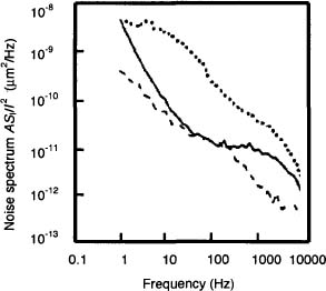
Figure 1. Noise spectra of three MOSFETs with active area of 0.4 μm2. Total number of the carriers in these samples is N ~ 103 (from Ref. 1 ).
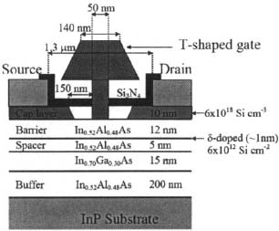
Figure 2. Cross-sectional schematic view of an InAIAs/lnGaAs MODFET with LG = 60 nm, W = 20 μm (from Ref. 2).
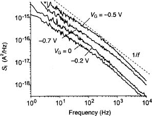
Figure 3. Frequency dependences of drain current fluctuations Sl in linear regime at different gate voltages VG. Dashed line shows the 1/f slope.2
Figure 3 demonstrates noise spectra of the drain current fluctuations at different gate voltage VG. At VG = 0, the number of carriers in the channel Ν ~ 31000, whereas at VG = –0.7 V, Ν ~ 3800. As can be seen from Fig. 3, the noise spectra demonstrate obvious 1/f behavior even at the smallest N value.
A recent publication reported the noise in GaN nanowires.3 Figure 4 shows field emission scanning electron microscopy (FESEM) images of GaN nanowires in the growth matrix, with diameter ranging from 50 to 200 nm. These GaN nanowires were processed into field effect transistors with a common gate (Si substrate) and symmetrically designed drain and source contacts (see inset in Fig. 5).
The number of carriers in the channel depended on substrate bias VG, dropping to N ~ 4 x 10³ at VG = 5.5 V. As seen in Fig. 5, noise spectra have l/f form (with some signature of separate Lorentzians in some samples).
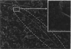
Figure 4. Field emission SEM images of GaN nanowires in the growth matrix. The inset shows a higher magnification image of the GaN nanowires.3
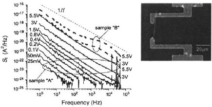
Figure 5. Frequency dependence of drain current fluctuations S in the linear regime for different VG values in a GaN nanowire transistor.3
The low frequency noise in single-walled carbon nanotubes (SWNTs), both metallic (M-SWNTs) and semiconducting (S-SWNTs), deposited on a Si substrate has also been reported – see Fig. 6.4 Again, the frequency dependence of spectral noise density is of the l/f form. No decomposition into separate Lorentzians has been observed even at substrate bias at which current through S-SWNTs was smaller than 10-11 A.
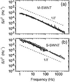
Figure 6. Frequency dependence of the relative current noise Sl//2 in the linear regime for M-SWNTs (a) and S-SWNTs (b).4
Low frequency noise was investigated in graphene single layer devices of 0.5 nm thickness, 1 μm length, and 20-200 nm width.5 The active volume V of smallest sample was about 10-17 cm-3.
Normalized current noise spectra Sl/I2 for two graphene devices with different widths, 20 and 200 nm, are shown in Fig. 7. The noise spectra show the characteristic 1/f dependence. In the 200 nm device, the noise amplitude is ~10 times lower than in the 20 nm device, in agreement with 1/V behavior, indicating that edge state scattering does not dominate the l/f noise.
Current noise power Sl at f = 10 Hz as a function of current I is shown in Figure 8 for the 20 nm wide graphene single layer device for different drain voltages VD. The observed I2 dependence indicates that current fluctuations are a manifestation of “volume” resistance fluctuations.
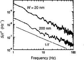
Figure 7. Frequency dependences of relative current noise S/l2 for single-layer graphene nanoribbons of 20 and 200 nm width.
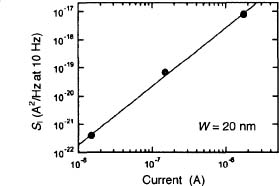
Figure 8. Current noise power Sl at f = 10 Hz vs. current / for a 20 nm wide single-layer graphene device. Drain voltages VD = 10 mV, 100 mV and 1 V. The current noise Sl ~ /2, indicating it is caused by resistance fluctuations.
Modem MOSFETs also demonstrate 1/f noise behavior. As mentioned, for example, in Ref. 6, the drain current noise of MOSFETs with LG = 30 nm and W = 10 μm (area A = 0.3 μm2) “shows a clear 1//noise behavior over which some Lorentzian G-R components may superimpose”.
As seen from results presented here, 1/f noise is observed in extremely small modern devices and therefore the funeral of 1/f noise is cancelled (or postponed).
3. Analysis and discussion
As seen in Fig. 1, if the gate area decreases and all other parameters are kept constant, the 1/f noise decomposes into separate Lorentzians. However, in any real device scaling rules dictate that other quantities should also change.
In MOSFETs, for example, a decrease in gate length LG must be accompanied by increase in channel electron concentration n (typically n ~ 1/LG, see, for example, Ref. 7). In the meantime, there is a well-established empirical rule that the concentration of defects nT is proportional (more or less) to the doping concentration n0. (That is not a decree of nature, but rather decree of technology). For this reason, the number of the defects in the channel remains virtually invariable as LG decreases: nT ~ nO ~ 1/LG. keeping the nTLG product constant.
Besides, according to scaling rules, decrease in gate length LG must be accompanied by a decrease in dielectric thickness tINS In modern MOSFETs with LG < 30 nm, tINS is down to a few nanometers (just several tens of atomic layers). Leakage current through such thin layers increases sharply and contributes to the total noise. Concentration of defects in such thin layers is much larger than that in “thick” oxide layers. Attempts to use thicker layers with higher dielectric constant (high-K layers) make the noise situation even worse: high-κ layers have higher trap concentrations which causes higher l/f noise.
Furthermore, it is necessary to take into account that as the size of the active region decreases, it becomes ever more difficult to discriminate between the “volume” and the “surface” of the device. Even if a very thin (several nanometers) “bulk” layer is totally defect-free, the surface states cause low frequency noise due to Coulomb interaction, surface roughness, and tunneling from “volume” to “surface” states.
Therefore, the funeral of the l//noise is at least postponed.
4. Conclusion
The prediction made several years ago about the disappearance of 1/f noise as “future” semiconductor devices decrease in size has failed. The main reason for this is the increase in defect concentrations due to downscaling of the devices. The use of new materials and processes also increases the defect concentration.
However, throughout the history of semiconductor devices, technological advances have gradually decreased the volume and surface defect densities. For example, Si technology started with 1015 cm-2 surface trap density decades ago, but nowadays can boast densities down to ~109 cm-2. Therefore, we can hope that the trap density in highly doped layers and high-κ dielectrics will decrease in the future. That gives us a hope for the end of the l//era in semiconductor devices.
Acknowledgments
This work was supported by Russian Foundation for Basic Research (grant 08-02-00010)
References
1. M. J. Uren, D. J. Day, and M. J. Kirton, “1/f and random telegraph noise in silicon metal-oxide-semiconductor field-effect transistors,” Appl. Phys. Lett. 47, 1196(1985).
2. M. E. Levinshtein, S. L. Rumyantsev, R. Tauk, et al., “Low frequency noise in InAlAs/InGaAs modulation doped field effect transistors with 50-nm gate length,” J. Appl. Phys. 102, 064506 (2007).
3. S. L. Rumyantsev, M. S. Shur, M. E. Levinshtein, A. Motayed, and A. V. Davydov, “Low-frequency noise in GaN nanowire transistors,” J. Appl. Phys. 103, 064501(2008).
4. A. Vijayaraghavan, S. Kar, S. Rumyantsev, et al., “Effect of ambient pressure on resistance and resistance fluctuations in single-wall carbon nanotube devices,” J. Appl. Phys. 100, 024315 (2006).
5. Z. Chen, Y. M. Lin, M. J. Rooks, and Ph. Avouris, “Graphene nano-ribbon electronics,” Physica E 40, 228 (2007).
6. T. Contaret, K. Romanjek, T. Boutchacha, G. Ghibaudo, and F. Boeuf, “Low frequency noise characterization and modeling in ultrathin oxide MOSFETs,” Solid State Electronics 50, 63 (2006).
7. M. S. Shur, Physics of Semiconductor Devices, New Jersey: Prentice Hall, 1990, pp. 353–396.