CHAPTER 3
INTRODUCTION TO THE PIC24 MICROCONTROLLER FAMILY
This chapter introduces the PIC24 instruction set architecture by exploring the data memory structure and data transfer instructions of the PIC24 microcontroller (μC). The use of the MPLAB® Integrated Design Environment for assembly and simulation of PIC24 programs is also discussed.
Learning Objectives
After reading this chapter, you will be able to:
![]() Describe the data and program memory architecture of the PIC24 μC.
Describe the data and program memory architecture of the PIC24 μC.
![]() Convert PIC24 instruction mnemonics to machine code and vice versa.
Convert PIC24 instruction mnemonics to machine code and vice versa.
![]() Describe the operation of the register direct, register indirect, immediate, file register, and default working register addressing modes.
Describe the operation of the register direct, register indirect, immediate, file register, and default working register addressing modes.
![]() Describe the operation of the
Describe the operation of the mov, add, sub, inc, inc2, dec, dec2, and goto instructions.
![]() Translate (manually compile) a simple C program into PIC24 assembly language.
Translate (manually compile) a simple C program into PIC24 assembly language.
![]() Compute the number of clock cycles and the amount of time required to execute simple instruction sequences for the PIC24 μC.
Compute the number of clock cycles and the amount of time required to execute simple instruction sequences for the PIC24 μC.
Introduction to Microprocessors and Microcontrollers
In the previous chapter, a computer was defined as a digital system composed of control, input/output, and memory components whose operation is controlled by instructions stored in memory. The first computers were designed in the early 1940s and filled entire rooms, with total processing capability that was less than a modern digital watch. Early computers used vacuum tubes (grossly, a current amplifier within a glass tube) to implement logic, and a single logic gate could take up an entire board. Transistors were invented by Bell Labs in 1947 [1], allowing an order of magnitude reduction in the size of a logic gate implementation. However, transistors were packaged individually, and computers still required a large number of circuit boards to implement. In 1958, Jack Kilby, a researcher at Texas Instruments Inc. created the first integrated circuit [1], which is a silicon substrate upon which circuits with multiple transistors can be fabricated (the slang term chip is now commonly applied to integrated circuits). As integrated circuit fabrication techniques evolved, the size of integrated circuit transistors steadily decreased, allowing increasing numbers of transistors to be placed on the same silicon substrate. In 1971, Intel® developed a set of four integrated circuits that implemented a 4-bit computer [1]. The data paths were 4 bits, much like the number sequencing computer of Chapter 2. One chip, the 4004, implemented the instruction decode and execution (the central processing unit, or CPU), while the other chips implemented the memory and input/output. The term microprocessor (μP) was applied to this chipset, as it was a very small (micro) processing engine. The 4004 chip is generally regarded as the world’s first microprocessor. Integrated circuit technology has continually improved since the 4004, producing two distinct paths of microprocessor evolution. One evolution path has stressed high performance, using the increasing number of transistors to build larger internal data paths (up to 64 bits) and registers, advanced numerical processing, and support for very large memory spaces. These microprocessors are referred to as general purpose microprocessors and expect programs and data to be stored in memory external to the microprocessor. General-purpose microprocessors require external support chips, known as a chipset, that allow them to interface with memory and input/output devices. Examples of general purpose microprocessors are the Intel Core™ i3/i5/i7, the Advanced Micro Devices FX, and the IBM PowerPC® families. Because of shrinking transistor size, it is now common to integrate multiple high performance CPUs on the same chip, as evidenced by the Intel Core™ i7 Extreme processor with six cores and the AMD FX processor with eight cores.
The other microprocessor evolution path has stressed higher integration and lower cost, with the goal of producing a single-chip solution to problems requiring a stored program machine approach. The term microcontroller (μC) is generally applied to these devices. A microcontroller typically expects its program and data to be stored on-chip, with any logic required for external input/output devices also integrated into the same device. Thus, a microcontroller implements all of the components of a computer—control, memory, and input/output—in one chip. Microcontroller solutions are usually very cost sensitive, so applying exactly the right amount of processing power to a problem to minimize cost is important. As such, a large number of microcontroller families are available from 8 bits to 32 bits, with widely varying amounts of on-chip memory and different combinations of input/output interface options (whose number and variety grow each year).
Microcontroller versions of general purpose microprocessors have also been introduced over the years, so the distinction between a microcontroller and a microprocessor has become somewhat blurred and in some cases is an arbitrary labeling. In this book, the term microcontroller is applied to devices in the PIC24 family, but the term microprocessor is used any time a more general labeling is desired.
The PIC24 Microcontroller Family
The PIC24 microcontroller family, created by Microchip Technology Inc., is the focus of this book for discussing microprocessor programming, architecture, and interfacing topics. At the time of this writing, the branches of the PIC24 family tree are the PIC24E, PIC24H, and the PIC24F. The PIC24E is the latest branch and is the highest speed with a maximum execution speed of 70 million instructions per second (MIPS) at 3.3V. The PIC24H family was the first “high-speed” branch and has a maximum execution speed of 40 MIPS. The PIC24F family is a lower-speed/lower-power variant that has a wide voltage operating range of 2.0 V to 3.6 V with a maximum execution speed of 16 MIPS. There are many versions of PIC24E/H/F microcontrollers available that differ in on-chip memory size, number of I/O pins, and on-chip peripheral features. However, all of the PIC24 family members use the same instruction set architecture (ISA). In fact, the PIC24 instruction set architecture is a subset of the dsPIC30/dsPIC33F/E ISA, another 16-bit microcontroller family from Microchip. The ds in dsPIC® stands for Digital Signal Processing (DSP), and dsPIC® microcontrollers have extra instructions implemented by an on-chip DSP engine that accelerate the types of computations found in DSP applications. The PIC24E and dsPIC33E families have the same on-chip peripherals and only differ in that the PIC24E does not have the DSP engine and thus does not support the additional DSP-oriented instructions. This book does not cover the extra instructions implemented by the DSP engine. In the hardware chapters of this book, the PIC24 microcontroller variant used for example purposes is the dsPIC33EPXXXGP502, which is pin compatible with the PIC24EPXXXGP202. The XXX indicates the program memory size in kilobinary bytes, with available sizes of 32, 64, 128, 256, and 512. The GP stands for general purpose. The last number of 202 (PIC24) and 502 (dsPIC33) indicates the packaging, which is a dual-in-line (DIP) 28-pin package in this case. When a specific example device is needed, the book uses the dsPIC33EP128GP502 microcontroller, but refers to all the dsPIC30/33 and PIC24 families as a PIC24 microcontroller. Your introduction to the PIC24 family begins with the instruction set architecture and a good place to start is with a simplified block diagram of the processor core, as shown in Figure 3.1.
Figure 3.1
PIC24 CPU core simplified architectural diagram (this is a simplified view of Figure 3.1 found in the PIC24EPXXXGP datasheet (DS70657G), Microchip Technology Inc.)
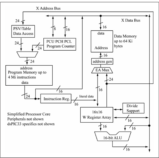
Source: Adapted with permission of the copyright owner, Microchip Technology, Incorporated.
All rights reserved. No further reprints or reproduction may be made without Microchip Inc.’s prior written consent.
The size of the internal data paths of the PIC24 CPU is 16 bits, so it is referred to as a 16-bit microcontroller. This means that the natural size for computations is 16 bits; arithmetic operations such as additions and subtractions that operate on 16-bit data or 8-bit data can be specified with one instruction. Operations on data larger than 16 bits can be performed but require multiple instructions to accomplish. The PIC24 instruction set defines 71 distinct instructions, of which the majority require 24 bits (3 bytes) to encode. The term instruction word is used to refer to a 24-bit machine code value. Two instruction types require two instruction words (6 bytes) to encode. The instruction register in Figure 3.1 contains the instruction word that is currently being executed. The arithmetic/logic unit (ALU) in Figure 3.1 is the combinational logic that performs operations such as addition, subtraction, bitwise AND/OR/XOR, and so forth. The left-side ALU input is from a register bank of 16 working registers named W0-W15, each of which is 16 bits wide. The right-side ALU input is connected to the X-data bus, which means that this operand can be from many different sources, with the most common sources being data memory or a working register. The ALU output is tied to the X-data bus, with the most common destination being data memory or a working register.
Program Memory Organization
Figure 3.1 shows that the PIC24 μC has separate memories for program instructions and data. This type of arrangement is known as a Harvard architecture, as early electromechanical calculators such as the Harvard Mark I [1] read instructions from punched tape, with memory used only for storing data. Most microprocessors store programs and data in the same memory, which means that instructions can access memory that contains instructions as easily as locations that contain data. The majority of PIC24 instructions can only access data memory; a few special mechanisms are provided enabling instructions to access program memory. The program counter (PC) is a 23-bit register that provides the address for accessing program memory for instruction fetch. Figure 3.2 illustrates how the PC value is used to access an instruction word in program memory. Even though an instruction word is 24 bits (3 bytes), it is actually more convenient to think of an instruction word as being 32 bits that consists of a least significant word (LSW) and most significant word (MSW), each 16 bits wide. The upper 8 bits of the most significant word are unimplemented and read as zeros; this is the phantom byte shown in Figure 3.2. In this model, program memory is addressable in 16-bit words, and the PC always points to the beginning of an instruction word, or the least significant word. This means that the least significant bit of the PC is always 0, and that the upper 22 bits of the PC contain the address of one instruction word out of a possible 222 = 4 Mi instruction locations. At the time of the writing of this text, no PIC24 microcontroller physically implemented the full 4 Mi instruction space supported by the architecture definition. Circa 2014, PIC24 family members offer a wide range of physical memory sizes ranging from 6 Ki instructions up to approximately 170 Ki instructions, with new variants being regularly introduced.
Program memory is nonvolatile, meaning the memory contents are retained when power is removed. Some form of nonvolatile memory is required for any practical computer system, as this provides the instructions that are executed when power is applied. The PIC24 program memory is flash programmable, meaning that it can be electrically erased and programmed. Other types of nonvolatile memory are one-time-programmable (OTP), meaning it cannot be erased once programmed, and mask-programmed read-only memory (ROM), which means the memory contents are determined at memory manufacture time and cannot be changed. Read operations on flash memory are fast, in the tens of nanoseconds, but write operations require more time with a minimum of 20 μs required to write one program word.
Figure 3.2
Program memory addressing (redrawn by author from Figure 4.6 found in the PIC24EPXXXGP datasheet (DS70657G), Microchip Technology Inc.)
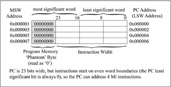
Source: Adapted with permission of the copyright owner, Microchip Technology, Incorporated.
All rights reserved. No further reprints or reproduction may be made without Microchip Inc.’s prior written consent.
Data Memory Organization
Figure 3.3 shows that the data memory address space is 64 KiB total, although additional memory may be accessed via a paging scheme not covered in this text. Data memory is organized as 16-bit words, with the lower 8 bits referred to as the least significant byte (LSB) and the upper 8 bits as the most significant byte (MSB). Observe that the LSB and MSB acronyms use a capital B in reference to byte; the acronyms LSb and MSb are reserved for least significant bit and most significant bit, respectively. Data memory is byte addressable, which means that the MSB and LSB portions of a 16-bit word can be modified individually. LSB addresses are at even locations, while MSB addresses are at odd locations. Data memory is volatile, meaning that its contents are lost if power is removed. Data memory is divided into the following sections:
![]() Special function registers. In the PIC24E/dsPIC33E family, the first 4096 locations of data memory (0x0000 to 0x0FFF) are reserved for special function registers (SFRs). An SFR is associated with some specific functionality implemented in the PIC24 μC. From an assembly language viewpoint, SFRs are treated in the same manner as a non-SFR data memory location, but their actual physical implementation is much different and depends upon the particular SFR. Most SFRs serve as data and control registers for on-chip peripherals such as the timers, the analog-to-digital converter, various serial interfaces, and so on. The W0-W15 working registers are SFRs, as well as the Program Counter. Even though each SFR is assigned a specific address, it is more common to refer to an SFR by its name rather than its location.
Special function registers. In the PIC24E/dsPIC33E family, the first 4096 locations of data memory (0x0000 to 0x0FFF) are reserved for special function registers (SFRs). An SFR is associated with some specific functionality implemented in the PIC24 μC. From an assembly language viewpoint, SFRs are treated in the same manner as a non-SFR data memory location, but their actual physical implementation is much different and depends upon the particular SFR. Most SFRs serve as data and control registers for on-chip peripherals such as the timers, the analog-to-digital converter, various serial interfaces, and so on. The W0-W15 working registers are SFRs, as well as the Program Counter. Even though each SFR is assigned a specific address, it is more common to refer to an SFR by its name rather than its location.
![]() Data RAM. Data memory locations that are not SFRs are referred to by various names such as file registers, data RAM, and X data. Data RAM is used for variable storage by user programs, but is also used as a side effect of instruction execution in some cases (i.e., the storage of a return address by a subroutine call, covered in Chapter 6). As with program memory, the amount of data RAM physically implemented is dependent upon the particular PIC24 μC. However, all PIC24 μCs have some amount of data RAM, and this begins at location 0x1000 for PIC24E/dsPIC33E devices.
Data RAM. Data memory locations that are not SFRs are referred to by various names such as file registers, data RAM, and X data. Data RAM is used for variable storage by user programs, but is also used as a side effect of instruction execution in some cases (i.e., the storage of a return address by a subroutine call, covered in Chapter 6). As with program memory, the amount of data RAM physically implemented is dependent upon the particular PIC24 μC. However, all PIC24 μCs have some amount of data RAM, and this begins at location 0x1000 for PIC24E/dsPIC33E devices.
![]() Near data memory. The first 8,192 locations in data memory are known as near RAM, and certain instruction forms can only access data memory locations in near RAM. Many PIC24 μC variants have physical data RAM that does not exceed the boundaries of near data space, and thus this distinction is not important in those devices. The assembly language examples in this text generally assume that all data RAM is located in near RAM. The dsPIC33EP128GP502 μC used in the hardware chapters of this text implements 16,384 bytes of data RAM, and thus a portion of its data RAM extends past near RAM. While 16,384 bytes of RAM seems tiny compared to the millions (and in many implementations, billions) of RAM bytes in a personal computer that contains a general purpose microprocessor, it is actually a generous data memory size for microcontrollers.
Near data memory. The first 8,192 locations in data memory are known as near RAM, and certain instruction forms can only access data memory locations in near RAM. Many PIC24 μC variants have physical data RAM that does not exceed the boundaries of near data space, and thus this distinction is not important in those devices. The assembly language examples in this text generally assume that all data RAM is located in near RAM. The dsPIC33EP128GP502 μC used in the hardware chapters of this text implements 16,384 bytes of data RAM, and thus a portion of its data RAM extends past near RAM. While 16,384 bytes of RAM seems tiny compared to the millions (and in many implementations, billions) of RAM bytes in a personal computer that contains a general purpose microprocessor, it is actually a generous data memory size for microcontrollers.
![]() Program space visibility area. The upper 32 Ki of data memory is also known as the program space visibility (PSV) area, which allows a user program to access non-volatile data stored in program memory. The PSV is discussed in more detail in Chapter 6.
Program space visibility area. The upper 32 Ki of data memory is also known as the program space visibility (PSV) area, which allows a user program to access non-volatile data stored in program memory. The PSV is discussed in more detail in Chapter 6.
![]() DMA RAM. Some PIC24 μCs have a portion of data RAM implemented as dual-port, static (DPS)RAM. The DPSRAM and associated DMA peripheral block allow some on-chip peripherals such as the analog-to-digital converter to transfer data to DMA RAM without intervention by the CPU core (i.e., without executing assembly language instruction for performing this data movement) and without slowing the CPU’s execution. Chapter 13 contains further discussion of DPSRAM and its usage.
DMA RAM. Some PIC24 μCs have a portion of data RAM implemented as dual-port, static (DPS)RAM. The DPSRAM and associated DMA peripheral block allow some on-chip peripherals such as the analog-to-digital converter to transfer data to DMA RAM without intervention by the CPU core (i.e., without executing assembly language instruction for performing this data movement) and without slowing the CPU’s execution. Chapter 13 contains further discussion of DPSRAM and its usage.
The sizes of program and data memories for some PIC24EP variants are listed in Table 3.1.
Table 3.1: Some PIC24EP Microcontroller Memory Sizes

Figure 3.3
Data memory organization for the PIC24EP128GP (redrawn by author from Figure 4.14 found in the PIC24EPXXXGP datasheet (DS70657G), Microchip Technology Inc.)
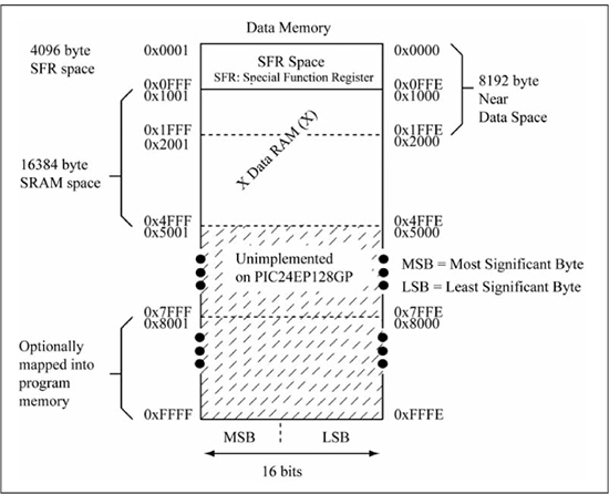
Source: Adapted with permission of the copyright owner, Microchip Technology, Incorporated.
All rights reserved. No further reprints or reproduction may be made without Microchip Inc.’s prior written consent.
Arrangement of Multibyte Values in Data Memory
This book’s assembly language and C programs use 8-bit, 16-bit, and 32-bit data sizes. Table 3.2 shows the unsigned ranges for these data sizes; Chapter 5 discusses signed data ranges for these same data sizes. As previously discussed, the lower byte of a 16-bit or 32-bit value is referred to as the least significant byte (LSB), while the upper byte is referred to as the most significant byte (MSB). Using a 16-bit or 32-bit variable instead of an 8-bit variable allows a larger number range to be represented, at the cost of requiring more data memory bytes.
When a 16-bit or 32-bit value is stored in data memory in the PIC24 μC, the bytes are arranged in least significant byte to most significant byte order in increasing memory locations. This arrangement is known as little-endian byte order, and it is in common use in many microprocessor implementations.
Table 3.2: Unsigned Data Ranges
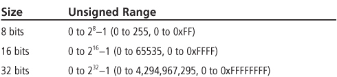
Some microprocessor families use the reverse arrangement of most significant byte to least significant byte in increasing memory locations, which is referred to as big-endian byte order. There is no inherent advantage to little-endian or big-endian byte order (computer architects have adopted these terms in a tongue-in-cheek reference to the book Gulliver’s Travels published by Jonathon Swift in 1726, in which Lilliputians and Blefuscans disagree over which end of the egg to crack first, the little end or the big end, when enjoying boiled eggs). The microprocessor architects determine the byte ordering choice during the microprocessor’s design phase. Figure 3.4 illustrates the storage of a 16-bit number and a 32-bit number in memory, with the memory shown in both 8-bit and 16-bit widths for additional clarity. Memory diagrams in this book always show memory addresses increasing as you progress down the page, and generally data memory is shown as 16 bits wide. The use of 32-bit data in assembly language programs is covered in Chapter 5.
Figure 3.4
Storage of multibyte data
A requirement of the PIC24 μC architecture is that 16-bit and 32-bit data must have the LSB start at an even location (i.e., be word aligned) if the data are to be accessed by PIC24 assembly language instructions in 16-bit chunks (also known as word mode). It is the responsibility of the assembly language programmer to ensure that 16-bit and 32-bit values are word-aligned in memory. A word access to an odd address is known as a misaligned access, which generates an exception that triggers execution of an exception handler, whose default action is to reset the processor (exceptions are covered in Chapter 9). A misaligned write operation does not alter data memory contents. The assembly language and C programs in this book assume that 16-bit and 32-bit values are correctly word-aligned in data memory. When writing assembly language programs by hand, it is often necessary to insert extra bytes in order to maintain this alignment.
Data Transfer Instructions and Addressing Modes
One fundamental instruction class found within any microprocessor is the data transfer class. Data transfer instructions copy data between registers and locations in data memory, or write a value stored in the instruction word into data memory or registers. In most microprocessors, registers are separate from data memory, and instructions contain addresses for both registers and memory. However, special function registers on the PIC24EP μC are simply data memory locations with addresses of 0x0000-0x0FFF, making the terms register and data memory location interchangeable. This is why data memory locations are sometimes referred to as file registers in the Microchip PIC24 μC documentation.
The execution of data transfer instructions between data memory locations is described as:
(src) → dst “copy the content of source location src to destination location dst.”
The → symbol is a transfer symbol, and (src) → dst is called register transfer notation, which is used to symbolically describe instruction execution. The parentheses () on the left side is read as “content of,” and indicates that you are transferring the content of a source memory location or register to a destination memory location or register. This is a common notation used to describe microprocessor instruction actions, and both register transfer notation and word descriptions are used in this book for discussing instruction execution.
Register Direct Addressing
For the PIC24 μC, instructions that copy data between data memory locations are called move instructions and the assembly language mnemonic is mov. This is somewhat unfortunate, as the word move implies removing data from one location and placing it in another location, but mov instructions do not affect the content of the source memory location. A mov instruction has two operands, source and destination, as noted earlier for data transfer operations. The two operands specify the addresses of the data to be moved. The method by which the address is specified is called the addressing mode. The simplest addressing mode is register direct, which specifies one of the 16 working registers. The following mov instruction copies the content of register W3 to W5:
mov W3, W5 ; copy the content of W3 to W5
Observe that for the PIC24 mov instruction, the first register is the source and the second register is the destination; other microcontroller instruction sets may reverse this order. In this book, lowercase is generally used for assembly language mnemonics and uppercase for register names (instruction mnemonics and working register names are actually case insensitive, so upper/lower case is used for emphasis only). The mov instruction has other addressing modes that are available for both source and destination operands, namely immediate, file register and six types of indirect addressing. This chapter provides examples of register direct, immediate, and file register addressing. One form of indirect addressing is discussed as well, with detailed coverage of the various indirect addressing modes reserved for Chapter 6. Because a register placeholder in an instruction format can be one of several different addressing modes, the following register placeholder symbols are used when discussing instruction formats:
![]() Wn: Register direct addressing; Wn specifies one of
Wn: Register direct addressing; Wn specifies one of W0, W1, ... W15.
![]() Wns: Register direct addressing; Wns specifies one of
Wns: Register direct addressing; Wns specifies one of W0, W1, ... W15.
![]() Wnd: Register direct addressing; Wnd specifies one of
Wnd: Register direct addressing; Wnd specifies one of W0, W1, ... W15.
![]() Wb: Register direct addressing; Wb specifies one of
Wb: Register direct addressing; Wb specifies one of W0, W1, ... W15.
![]() WREG: The working register; specifies
WREG: The working register; specifies W0 in file register instructions.
![]() Ws: Register direct (Ws) and indirect addressing modes ([Ws], [Ws ++], [Ws – –], [++Ws], [– –Ws]); Ws specifies one of
Ws: Register direct (Ws) and indirect addressing modes ([Ws], [Ws ++], [Ws – –], [++Ws], [– –Ws]); Ws specifies one of W0, W1, ... W15.
![]() Wd: Register direct (Wd) and indirect addressing modes ([Wd], [Wd ++], [Wd – –], [++Wd], [– –Wd]); Wd specifies one of
Wd: Register direct (Wd) and indirect addressing modes ([Wd], [Wd ++], [Wd – –], [++Wd], [– –Wd]); Wd specifies one of W0, W1, ... W15.
![]() Wso: All of the addressing modes of Ws, with the additional mode of register offset indirect [Wso + Wb]; Wso specifies one of
Wso: All of the addressing modes of Ws, with the additional mode of register offset indirect [Wso + Wb]; Wso specifies one of W0, W1, ... W15.
![]() Wdo: All of the addressing modes of Wd, with the additional mode of register offset indirect [Wdo + Wb]; Wdo specifies one of
Wdo: All of the addressing modes of Wd, with the additional mode of register offset indirect [Wdo + Wb]; Wdo specifies one of W0, W1, ... W15.
For example, the general form of the previous move instruction is mov Wso, Wdo with each operand able to use seven different addressing modes. Examples are:
mov W2, W3            ; both source and destination use reg. direct
mov [W2], [W3 + W7]   ; both source and destination use reg. indirect
mov [--W4], W5        ; source uses reg. indirect, dest. uses reg. direct
As previously mentioned, only one indirect addressing mode is discussed in this chapter; the remaining modes are reserved for Chapter 6.
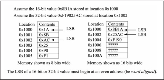
The previous mov instruction operates in word mode; that is, the 16 bits in W3 are copied to W5. Word mode operation is the default for instructions, and the mnemonic can be written with a .w extension if desired:
mov.w W3, W5 ; copy the content of W3 to W5
A byte mode is also available, and must be specified with a .b extension as follows:
mov.b W3, W5 ; copy the content of W3.LSB to W5.LSB
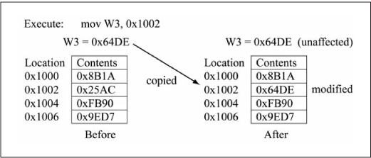
In this case, only the LSB of W3 is copied to the LSB of W5; the MSB of W5 is unaffected. This book uses the notation Wn.LSB and Wn.MSB to refer to the least significant and most significant bytes of register Wn, respectively. Figure 3.5 shows another example of a mov using register direct addressing.
Figure 3.5mov using register direct addressing
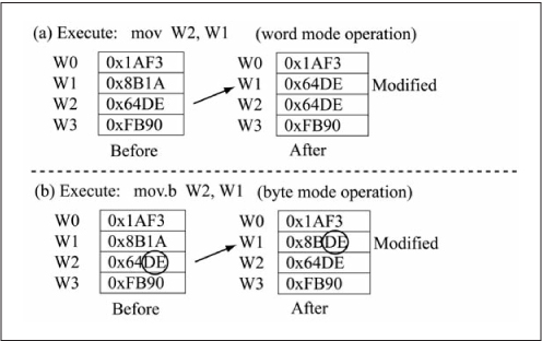
Figure 3.6(a) gives the instruction format for the mov.{b} Wso, Wdo instruction. Observe that the ssss bit field in the instruction format specifies the Wso register number, while the dddd bit field specifies the Wdo register number. The ggg and hhh fields specify the addressing modes of the source and destination operands, respectively. The wwww field is only used if a particular form of indirect addressing is used (register offset indirect). Figure 3.6(b) shows the conversion of the mov W3, W5 instruction to its machine code representation of 0x780283. The 3-bit code for register direct addressing is 0b000 (see Appendix A), which is used for the ggg, hhh fields since both the source and destination of the mov W3, W5 instruction uses register direct addressing. The wwww field is unused and can be set to 0b000 because register direct addressing, rather than indirect addressing, is used. The machine code for the mov.b W3, W5 instruction is given in Figure 3.6(c) with the B-field bit (byte versus word operation) being the only difference from Figure 3.6(b).
This text does not attempt to discuss the instruction formats of every PIC24 instruction, but instead covers the formats of a few select instructions from the different classes of PIC24 instructions. A table of the machine code formats for all PIC24 instructions can be found in Appendix A.
Figure 3.6
Instruction format: mov{.b} Wso, Wdo

File Register Addressing
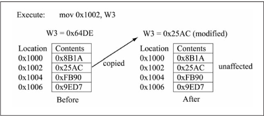
File register addressing specifies a data RAM address encoded as part of the instruction machine code (in other microprocessor families, this type of addressing is called memory direct addressing, since the memory address is directly specified in the instruction word). Figure 3.7(a) shows the instruction format for a mov instruction whose source operand uses register direct addressing and whose destination operation uses file register addressing. This mov form only operates in word mode, so the file register address must be an even address to satisfy the word-alignment rules previously discussed. Because the file register address is word-aligned, its lower bit must be zero, so only the upper 15 bits of the 16-bit address are encoded in the instruction. The conversion of mov W3, 0x1002 to machine code is given in Figure 3.7(b).
Figure 3.8 shows the operation of a mov W3, 0x1002 instruction in word mode, causing the bytes in locations 0x1002 and 0x1003 to become copies of W3.LSB and W3.MSB, respectively.
Figure 3.7
Instruction format: mov Wns, f
Figure 3.8
Example operation: mov Wn, f
Given that there is a method for copying data from a working register to data RAM, it follows that the converse must be possible. Figure 3.9 shows the execution of the mov 0x1002, W3 instruction, which copies the content of data RAM location 0x1002 to W3. The general form of this mov form is mov f, Wn and it also can only function in word mode. See Appendix A for the machine code format of this mov type.
Figure 3.9
Example operation: mov f, Wn
WREG—The Default Working Register
The astute reader may be wondering at this point how to transfer a byte between a working register and data RAM, since the mov Wn, f and mov f, Wn instructions only operate in word mode. Byte transfers between working registers and data memory are accomplished by either using the indirect addressing modes (Chapter 6) or by using a mov instruction form that uses the default working register. The mov{.b} WREG, f instruction format is shown in Figure 3.10. There are two important points about this instruction format. First, the default working register (WREG) is W0. Second, because only 13 bits are reserved for the data memory address, f has to be in the first 8192 locations (213 = 8192) of data memory. As previously discussed, this area of data RAM is known as near RAM. Any PIC24 instruction that uses WREG and a file register address has this near RAM restriction.
Figure 3.11 illustrates a byte transfer from the LSB of W0 to memory location 0x1001 using the mov.b WREG, 0x1001 instruction. While WREG is synonymous with W0 in terms of instruction execution, it is a syntax error to write this instruction form as mov.b .W0, 0x1001
Figure 3.10
Instruction format: mov{.b} WREG, f
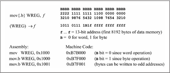
Figure 3.11
Example operation: mov{.b} WREG, f

To transfer the LSB of any other working register besides W0 to data RAM, execute a two-instruction sequence:
mov.b  Wn, W0       ; move the Wn.LSB to W0.LSB
mov.b  WREG, f      ; move W0.LSB to data memory
Figure 3.12 shows the format of the mov{.b} f {, WREG} instruction, which copies from a data memory location to either the WREG or back to itself. Observe that the D bit in the machine code selects between a destination of WREG (D bit = 0) or f (D bit = 1). At this point it may seem pointless to copy a data RAM value back to itself, but the usefulness of this operation is discussed in Chapter 4. Figure 3.13 shows an example operation of mov{.b} f {, WREG} for the case of mov.b 0x1000, WREG.
Figure 3.12
Instruction format: mov{.b} f {, WREG}
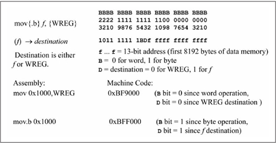
Figure 3.13
Example operation: mov{.b} f {, WREG}
Immediate Addressing
The immediate addressing mode encodes a literal (a constant) in the instruction word. Figure 3.14 shows the instruction format for immediate addressing used in a mov instruction to load a working register with a constant. The constant is a 16-bit value if a word operation is performed and an 8-bit value if a byte operation is done. The instruction encoding is such that these are actually two different opcodes with the instruction encoding that is used dependent on the literal size.
Figure 3.14
Instruction format: mov #lit16, Wn; mov.b #lit8, Wn
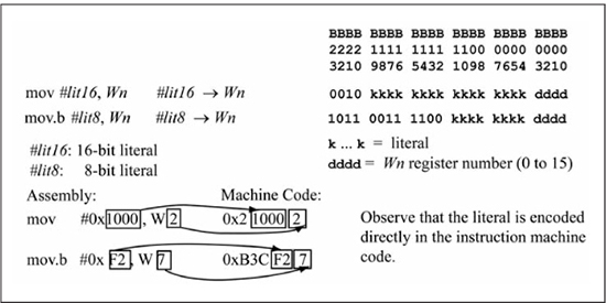
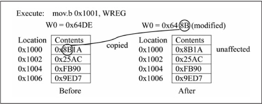
It is common for a reader new to assembly language programming to confuse immediate addressing with file register addressing. The difference between these two addressing modes is illustrated in Figure 3.15. In Figure 3.15(a), the mov #0x1000, W2 instruction (immediate addressing) copies the value 0x1000 into register W2. Contrast this with Figure 3.15(b), where the mov 0x1000, W2 instruction copies the word located at data RAM location 0x1000 into W2, resulting in a modified W2 value of 0x8B1A. The # symbol used with 0x1000 differentiates immediate addressing from file register addressing. Figure 3.15(c) illustrates execution of a mov instruction that uses an 8-bit literal; observe that only the LSB of W2 is affected. If a word operation is used in Figure 3.15(c), then all 16-bits of W2 are written.
Figure 3.15
Instruction format: mov{.b} #lit, Wn

Indirect Addressing
A mov that uses one of the many forms of indirect addressing for both source and destination operands is:
mov [Wns], [Wnd] ; ((Wns)) → (Wnd)
Compare this with a mov that uses register direct addressing for both operands:
mov Wns, Wnd ; (Wns) → Wnd
Note that the operands for the indirect addressing example use brackets [] around the Wns and Wnd operands, indicating an indirect addressing mode. The register transfer description for the indirect example has an extra set of parentheses () around both the Wns and Wnd operands. The ((Wns)) → (Wnd) register transfer operation means the following:
![]() The content of
The content of Wns, also written as (Wns), is an address called the source effective address, abbreviated as EAs. The content of the source effective address, written as (EAs), is the source operand. Thus, the source operand is fully specified as ((Wns)).
![]() The content of
The content of Wnd, also written as (Wnd), is an address called the destination effective address, abbreviated as EAd. The mov copies the source operand to the memory location specified by the destination effective address, or in register transfer notation: (EAs) → EAd or ((Wns)) →(Wnd).
A mov instruction that uses indirect addressing for one or both of its operands has an instruction format much like the mov instructions that use immediate or direct addressing modes discussed earlier. The details of the instruction format for indirect addressing mov instruction are left as an exercise for you.
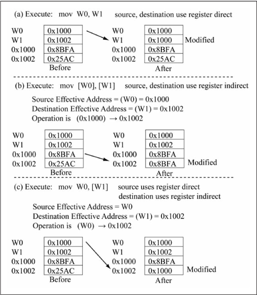
Figure 3.16 shows three mov instruction examples. Figure 3.16(a) shows a mov instruction; note that this uses register direct addressing for both source and destination operands. The end result of Figure 3.16(a) is that the content of W0, W1W0 is copied to W1, modifying W1 to contain 0x1000. Figure 3.16(b) shows a mov [ instruction that uses register indirect addressing for both source and destination operands. The source operand’s effective address is the content of W0], [W1]W0, or 0x1000. The destination effective address is the content of W1, or 0x1002. Thus, the mov’s execution copies the content of location 0x1000 to location 0x1002, modifying location 0x1002 to contain 0x8BFA. The final example in Figure 3.16(c) shows a mov instruction, illustrating that different addressing modes can be used for the source (register direct) and destination (register indirect) operands. The W0, [W1]mov instruction’s execution copies the content of W0 to the destination effective address, which is the content of W1 (0x1002 as seen in the figure), thus modifying location 0x1002 to contain 0x1000.
There are other types of indirect addressing modes; these are reserved for Chapter 6 as indirect addressing is better appreciated when discussed in the context of pointer operations in the C language.
Figure 3.16
Example operation: mov.{b} [Wns], [Wnd]
Instruction Set Regularity
At this point you might be somewhat dizzy from the number of different mov types that have been covered and also fearful of the remaining 70 instructions yet to be discussed. In an attempt to put your mind at ease, we assert that you will soon discover that there is a regularity to the PIC24 instruction set architecture. This means that once the rules are understood for one instruction class, the same rules apply to other instructions in the same class. The number of instruction classes is small, so there are not very many different rule sets that must be understood. Rest assured that the task is not as difficult as it may seem at this particular point!
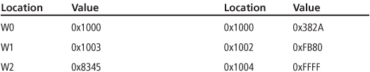
Sample Question: Assume that registers and memory contain the values of Table 3.3 at the start of each of the following instructions. Give the register or memory location that is modified by the instruction and its new value.
Table 3.3: Register Memory Contents
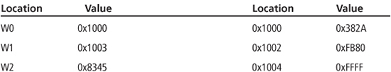
1. mov W2, W0
2. mov 0x1000, W0
3. mov #0x1000, W0
4. mov W2, [W0]
5. mov.b W2, W0
6. mov W2, [W1]
7. mov 0x1000, WREG
8. mov 0x1000
Answers:
1. This performs (W2) → W0, or 0x8345 → W0, so W0 is modified to 0x8345.
2. This performs (0x1000) → W0, or 0x382A → W0, so W0 is modified to 0x382A.
3. This performs 0x1000 → W0, so W0 is modified to 0x1000.
4. This performs (W2) → (W0), or 0x8345 → 0x1000, so location 0x1000 is modified to 0x8345.
5. This performs (W2.LSB) → W0.LSB, so W0 is modified to 0x1045.
6. This performs (W2) → (W1), or 0x8345 → 0x1003, which is an illegal operation because a word operation is being done to an odd address. Location 0x1003 is not modified, and a misaligned address exception is generated (Chapter 9).
7. This performs (0x1000) → WREG, or 0x382A → W0, so W0 is modified to 0x382A.
8. This performs (0x1000) → 0x1000, or 0x382A → 0x1000, location 0x1000 is left unchanged as 0x382A.
Basic Arithmetic and Control Instructions
Two other classes of microprocessor instructions are arithmetic and control classes. All microprocessors have arithmetic instructions such as addition, subtraction, increment (+1), and decrement (–1) instructions. Some microprocessors, such as the PIC24, also have instructions for multiplication and division; these can be implemented using addition, subtraction, and shifts if dedicated multiplication and division instructions are not present.
Three-Operand Addition/Subtraction
The PIC24 supports both a three-operand form and a two-operand form for addition and subtraction operations. The first three-operand forms to be discussed are:
add{.b} Wb, Ws,  Wd     ; (Wb) + (Ws) → Wd
sub{.b} Wb, Ws,  Wd     ; (Wb) – (Ws) → Wd
subr{.b} Wb, Ws, Wd     ; (Ws) – (Wb) → Wd
Recall that the Ws, Wd symbols allow both register direct and register indirect addressing modes (with the exception of register offset indirect). The Wb operand is limited to register direct addressing. Examples of different addressing mode forms for these instructions are:
add W2, [W8], W3           ; reg. indirect for Ws, reg. direct for Wd
sub.b W3, W4, W5           ; reg. direct for Ws, Wd
subr W9, [W4++], [  W8]    ; these indirect modes are covered in Chapter 6
The advantage of a three-operand addition or subtraction is that the values of the two source operands can be preserved if desired. Figure 3.17 shows three addition examples using register direct addressing. Figure 3.17(a) illustrates execution of the add instruction, while Figure 3.17(b) shows the same operation in byte mode. Figure 3.17(c) demonstrates that the three operands can be any of the working registers, including having all three operands from the same register.W0, W1, W2
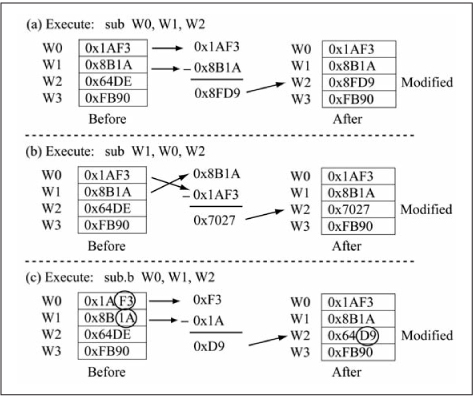
Three subtraction examples are given in Figure 3.18. Because subtraction is not commutative, the instructions sub and W0, W1, W2sub W1, are not mathematically equivalent. When using a subtraction instruction, you must remember that W0, W2sub Wb, Ws, Wd implements (Wb) - (Ws) and not vice versa, as shown in Figures 3.18(a) and 3.18(b). Byte mode operation for subtraction is shown in Figure 3.18(c). The subr instruction forms perform the reverse subtraction operation, so subr Wb, Ws, Wd implements (Ws) - (Wb).
The three-operand forms for addition/subtraction using immediate addressing are:
add{.b} Wb, #lit5,  Wd     ; (Wb) + #lit5 → Wd
sub{.b} Wb, #lit5,  Wd     ; (Wb) – #lit5 → Wd
subr{.b} Wb, #lit5, Wd     ; #lit5 – (Wb) → Wd
Figure 3.17
Instruction execution: add{.b} Wb, Ws, Wd
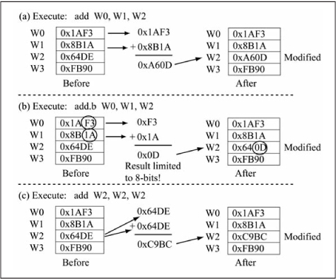
Figure 3.18
Instruction execution: sub{.b} Wb, Ws, Wd
The #lit5 operand is a 5-bit unsigned literal, meaning the number range that can be encoded is 0 to 31. When this 5-bit unsigned literal is used in an operation with an 8-bit or 16-bit operand, its upper bits are filled with zeros to match the length of the other operand. This is known as zero extension, and this is discussed in more detail in Chapter 4. The previous addition and subtraction instructions are limited to a 5-bit literal because of the number of available bits in the 24-bit instruction word after the base register Wb and destination register Wd locations are encoded. Indirect addressing modes can be used with the Wd operand, while the Wb operand is limited to register direct addressing. These instructions form a convenient mechanism for adding or subtracting a small constant using a single instruction. A larger constant can be added or subtracted by the two-instruction sequence:
mov #lit16, Wx        ; #lit16 → Wx
add/sub  Wb, Wx, Wd  ; Wb  +/- Wx → Wd
Two-Operand Addition/Subtraction
The two-operand addition/subtraction forms use file register addressing and the default working registers as follows:
add{.b}  f           ; (f) + (WREG) → f
add{.b}  f, WREG     ; (f) + (WREG) → WREG
sub{.b}  f           ; (f) – (WREG) → f
sub{.b} f, WREG      ; (f) – (WREG) → WREG
subr{.b} f           ;(WREG) – (f) → f
subr{.b} f, WREG     ;(WREG) – (f) → WREG
As with the mov form that used these addressing modes, the data RAM address f must be in near RAM (the first 8192 locations). The advantage of the two-operand addition/subtraction forms is that a value can be added to a data memory location without first copying that location’s value into a working register. The disadvantages of the two-operand addition/subtraction forms are that one of the source operands must be overwritten (destroyed) and the restriction to near memory for the data memory address.
Two-operand addition/subtraction using immediate addressing and register direct addressing are:
add{.b} #lit10, Wn     ; (Wn) + #lit10 → Wn
sub{.b} #lit10, Wn     ; (Wn) – #lit10 → Wn
The #lit10 operand is a 10-bit unsigned literal whose range is 0 to 1023 for word operations and 0 to 255 for byte operations. These instructions forms are limited to register direct addressing for the Wn operand; there is not a subr form available.
Increment, Decrement Instructions
Various increment and decrement instructions are provided; the first forms to be discussed are:
inc{.b} Ws,  Wd     ;(Ws) + 1 → Wd
inc2{.b} Ws, Wd     ;(Ws) + 2 → Wd
dec{.b} Ws,  Wd     ;(Ws) – 1 →  Wd
dec2{.b} Ws, Wd     ;(Ws) – 2 →  Wd
These increment/decrement instructions use register direct and register indirect addressing modes for the source and destination operands. The inc2/dec2 instructions provide increment/decrement by 2 instead of by 1, which is useful when you’re incrementing a register containing a data memory address and want the address to be incremented to the next 16-bit location. You might wonder why these instructions are included when it appears that the same functionality can be accomplished by use of the add/sub instructions using the short literal (#lit5). The answer is that the indirect modes available for the source operand (Ws) in the increment/decrement instructions provide more flexibility than add/sub instructions with a short literal. If the source operand uses register direct addressing, then there is no advantage either way in using the increment/decrement instructions versus using the add/sub instruction with a short literal.
Some additional forms of increment/decrement that use file register direct and the working register are:
inc{.b} f              ;(f) + 1 → f
inc{.b} f, WREG        ;(f) + 1 → WREG
inc2{.b} f             ;(f) + 2 → f
inc2{.b} f, WREG       ;(f) + 2 → WREG
dec{.b} f              ;(f) – 1 → f
dec{.b} f, WREG        ;(f) – 1 → WREG
dec2{.b} f             ;(f) – 2 → f
dec2{.b} f, WREG       ;(f) – 2 → WREG
As previously seen with the mov instruction using this addressing mode, f is limited to near RAM, the lowest 8192 locations in data memory.
Program Control: goto
Control instructions affect the program counter content, with the simplest form being a goto, an unconditional transfer of control. Figure 3.19 shows the machine code format for the goto instruction.
The nnn ... nn bits encoded in the goto machine code shown in Figure 3.19 specify the program memory location that control is transferred to, which is known as the target address. The nnn ... nn bits form a 22-bit value that specifies one of the 4 Mi (222) possible instruction word locations; this 22-bit value is concatenated with a 0 bit to form a 23-bit value that is loaded into the 23-bit program counter.
Figure 3.19
Instruction format: goto Expr
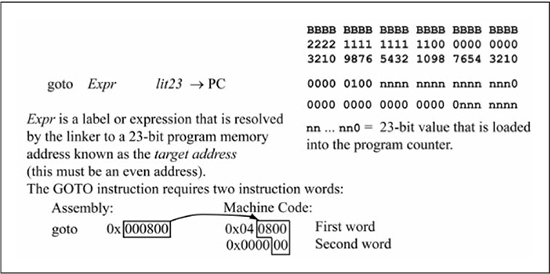
The goto instruction requires two instruction words (6 bytes), with the second instruction word containing bits 22 through 16 of the target address and the first instruction word containing the remaining bits of the target address. There is only one other instruction in the PIC24 instruction set that requires two instruction words to encode (a call instruction) and it also specifies a target address in the program address space. The call instruction is also in the control class; and its usage is covered in Chapter 6.
Sample Question: Assume that registers and memory contain the values of Table 3.4 at the start of each of the following instructions. Give the register or memory location that is modified by the instruction and its new value.
Table 3.4: Register Memory Contents
1. add W2, W1, W0
2. add 0x1000, WREG
3. sub.b W0, #5, W1
4. inc [W0], W1
5. dec.b W0, [W1]
7. dec2.b W2, W1
8. inc 0x1004
Answers:
1. This performs (W2) + (W1) → w0, or 0x8345 + 0x1003 → w0, so w0 is modified to 0x9348.
2. This performs (0x1000) + w0 → w0, or 0x382A + 0x1000 → w0, so w0 is modified to 0x482A.
3. This performs (w0.LSB) – 5 → W1.LSB, or 0x00 – 5 → W1.LSB, so W1 is modified to 0x10FB.
4. This performs ((w0)) + 1 → W1, or (0x1000) + 1 → W1, or 0x382A + 1 → W1, so location W1 is modified to 0x382B.
5. This performs (w0.LSB) – 1 → (W1), or 0x00 – 1 → 0x1003, so 0x1003 is modified to 0xFF. The word at location 0x1002 now reads as 0xFF80.
6. This performs (W2) – ((w0)) → (w0), or 0x8345 – (0x1000) → 0x1000, or 0x8345 – 0x382A → 0x1000, so location 0x1000 is modified to 0x4B1B.
7. This performs (W2.LSB) – 2 → W1.LSB, or 0x45 – 2 → W1.LSB, so W1 is modified to 0x1043.
8. This performs (0x1004) + 1 → 0x1004, or 0xFFFF + 1 → 0x1004, location 0x1004 is modified to 0x0000 (0xFFFF + 1 wraps back to 0x0000).
A PIC24 Assembly Language Program
At this point, you have more than enough instructions to write a simple PIC24 assembly language program. In this book, programs are first written in C then translated (compiled) to assembly language. This is done for the instructional purpose of illustrating the linkage between high-level programming language statements and their implementation in assembly language. Furthermore, programs written in a high-level language such as C improves the clarity of the program’s functionality, as assembly language can be obtuse, especially for readers new to assembly language programming. This also prepares you for the hardware interfacing chapters of this book, which uses the C language for all its example programs. If you are new to the C language, do not worry, as C language statements are introduced gradually and are fully explained. A previous exposure to any modern programming language is all that is necessary to understand the C program examples used in this book. Example C programs only use those C language statements necessary to demonstrate PIC24 μC capabilities and do not attempt to cover the entire C language. A program called a compiler is generally used to perform the translation from C to assembly language. This book uses the MPLAB XC16 compiler for this task when C programs illustrating microcontroller hardware interfacing are covered beginning in Chapter 8.
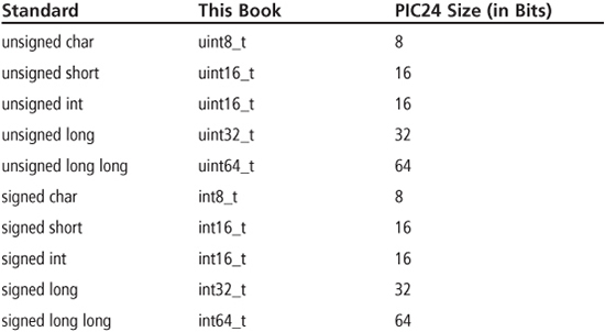
Table 3.5 shows the standard C data types of char, short, int, long, and long long in their unsigned and signed varieties and how these types are referred to in this book. The standard C types represent different sized variables, with a char variable always requiring 8 bits (1 byte). A problem with the standard C data types is that the sizes of the int and long types are compiler-dependent. For example, in the C compiler used in this book for the PIC24 μC, the int and long types are 16 bits and 32 bits. However, these same types may be 32 bits and 64 bits for a different processor/compiler combination, which can create issues when porting C code. To address this problem, the C99 C standard (ISO/IEC 9899:1999) defined new integer data types that explicitly state the number of bits for each type. It has become common practice for C programmers, especially when writing code for microcontrollers, to use these new types because variable size affects both data and program storage requirements, along with program execution time. So, referring to Table 3.5 for an example, an unsigned int variable is declared as a uint16_t variable in any C program used in this book.
C-to-PIC24 Assembly Language
A C program that uses the data transfer and arithmetic operations discussed so far is shown in Listing 3.1. Line numbers have been added for clarity, but would not be part of the actual C program source code.
Listing 3.1: A “Simple” C Program
(1)       uint8_t u8_i, u8_j, u8_k;

(2)       void main(void) {
(3)         u8_i = 100;           // u8_i = 100 (0x64)
(4)         u8_i = u8_i + 1;      // u8_i++, u8_i = 101 (0x65)
(5)         u8_j = u8_i;          // u8_j is 101 (0x65)
(6)         u8_j = u8_j - 1;      // u8_j , u8_j is 100 (0x64)
(7)         u8_k = u8_j + u8_i;   // u8_k = 201 (0xC9)
(8)       }
The C language is case sensitive, with all reserved keywords, such as void, being lowercase. Comments begin with two // characters and can start anywhere on a line (this is actually a C++ language comment now included in the C99 standard, so it is accepted by modern C compilers). Comments can also be delimited by a starting /* and an ending */ with the delimiters spanning multiple lines. Simple C statements are terminated by a semicolon (;). Compound statements, which are composed of multiple simple C statements, are bracketed by {}. Line 1 defines three variables of type uint8_t, which from Table 3.5 means that each variable is 8 bits, or 1 byte, and represents unsigned data (unsigned char). The unsigned modifier tag combined with the 8-bit data size gives a value range of 0 to 255 for each variable. Chapter 5 discusses the difference between unsigned and signed data types and the effect this has on arithmetic operations. C code examples in this text use prefixes (i.e. u8_) as part of variable names as a strong hint of their data type in order to improve code readability. Line 2 defines the entry point for the C program, which must be named main. The (void) before the main label indicates that this main function returns no value, which will always be the case in this book. The (void) after the main label indicates that main receives no parameters, which will always be the case for C programs in this book (Chapter 6 discusses the details of parameter passing and value return for C functions in more detail). The body of the main code is a compound C statement, enclosed by {}. Line 3 assigns the constant value 100 to the variable u8_i. Line 4 increments u8_i by 1; u8_i contains the value 101 after execution of this statement. The C statement u8_i++, where ++ is the C increment operator, could be used instead of u8_i= u8_i + 1. Line 5 copies the value of u8_i to u8_j. Line 6 decrements u8_j, so u8_j contains the value 100 after execution of this statement. The statement u8_j-- could be used instead of u8_j= u8_j - 1. Line 7 adds u8_j to u8_i and places the result in u8_k.
The first step in translating (i.e., compiling) the program in Listing 3.1 to PIC24 assembly language is to choose locations for the variables u8_i, u8_j, and u8_k. This can be any data RAM location that is not assigned to a special function register. You could also simply use working registers to represent variables, and you’ll see how to do this when C functions are covered in Chapter 6. This example uses data RAM for variables. For simplicity, the example uses the first available data RAM locations, which are 0x1000 for u8_i, 0x1001 for u8_j, and 0x1002 for u8_k (recall that data RAM locations 0x0000 through 0x0FFF are reserved for special function registers). Figure 3.20 shows the program of Listing 3.1 translated to PIC24 assembly language.
Figure 3.20
The contents of main in the “simple” C program compiled to PIC24 assembly language

The compilation is straightforward when only one line is considered at a time. Optimizing C compilers (and expert assembly language programmers) consider multiple C language statements at a time during compilation in an effort to reduce the total number of instructions, and it may be difficult to correlate the final assembly code with the original C language statements. This book does not expect you to become an expert assembly language programmer; this only occurs after a considerable amount of time is spent crafting assembly language programs. Instead, this book strives for clarity and understanding, so it will always perform C-to-PIC24 assembly language translation in the most straightforward manner possible. Some comments on the assembly code in Figure 3.20 are:
![]() Byte operations (
Byte operations (.b) are used because u8_i, u8_j, and u8_k are uint8_t (1 byte) variables.
![]() You might wonder why both
You might wonder why both W0 and WREG are used in the assembly language for the first C statement u8_i = 100. Only WREG can be used in a mov instruction that is a byte operation and specifies a file register address, so the destination for the constant value 100 must be specified as WREG. However, the mov instruction with an immediate operand requires one of the working registers, W0 through W15, as its destination. It is a syntax error to write mov.b #100, WREG and also a syntax error to write mov.b even though W0,iW0 and WREG are physically the same register.
![]() You might wonder why the assembly statement
You might wonder why the assembly statement mov.b 0x1000, 0x1001 is not used for the u8_j = u8_i operation. The answer is simple—there is no PIC24 mov instruction that allows file register addresses to be specified for both the source and destination operands. Instead, u8_i must be copied to a working register first, and then copied from the working register to u8_j.
Of the C language statements in Figure 3.20, the statement u8_k = u8_j + u8_i is the most difficult, and this implementation uses five PIC24 instructions. The first step copies the operands u8_i and u8_j to registers W1 (u8_i) and W0 (u8_j). Copying u8_i to W1 required two instructions (mov.b 0x1000, WREG followed mov.b ) because a byte operand can only be copied into W0, W1WREG (W0) from data memory. The code then uses a three-operand add instruction for the addition, placing the result into W0. Using W0 for the result was done because the result is copied to operand u8_k with the next instruction, and only WREG (W0) can be used for a byte copy to data memory. Observe that the instruction add.b W0, W1, W0 can be replaced by add.b W1, W0, W0 since addition is commutative (u8_j + u8_i is the same as u8_i + u8_j). You could have also used a different register such as W2 to hold u8_i; the choice is arbitrary.
Listing 3.2 shows an alternate implementation for u8_k = u8_i + u8_i that requires only three instructions as it uses the two-operand form of the add instruction. Typically, use of two-operand ALU instructions requires fewer instructions for implementing small C code fragments. Unfortunately, we have found that new assembly language programmers make mistakes more often using two-operand ALU instruction forms as they forget which register is the source and which is the destination as well as forgetting that one of the operands is overwritten by the result. As such, the assembly language examples will often sacrifice instruction efficiency by using three-operand ALU instruction forms for extra clarity. In many cases, we will show different assembly language implementations for the same C code fragment to illustrate that there are multiple approaches. We stress that new assembly language programmers should use the approach that they best understand and strive for code efficiency once coding experience has been gained.
Listing 3.2: Alternate Implementation of u8_k = u8_j + u8_i
mov.b 0x1000, WREG      ;WREG = u8_i
add.b 0x1001, WREG      ;WREG = u8_j + WREG = u8_j + u8_i
mov.b WREG, 0x1002      ;u8_k = WREG = u8_j + u8_i
Listing 3.3 shows an implementation for the C language statement u8_k = u8_j - u8_i with the only difference from the code in Figure 3.20 being the use of a three-operand sub instruction instead of the add instruction. Observe that the instruction sub.b W0, W1, W0 cannot be replaced by sub.b W1, W0, W0 since subtraction is not commutative (u8_j - u8_i is not the same as u8_i - u8_j).
Listing 3.3: Implementation of u8_k = u8_j – u8_i
mov.b 0x1000, WREG ; WREG = u8_i mov.bW0, W1 ; W1 = u8_i mov.b 0x1001, WREG ; WREG = u8_j sub.bW0, W1,W0;W0=W0- W1 = u8_j - u8_i mov.b WREG, 0x1002 ; u8_k = WREG = u8_j - u8_i
The code in Figure 3.20 makes heavy use of WREG because of the need for byte operations to data memory and the use of file register addressing. There are many other possible assembly language implementations using addressing modes such as indirect addressing, but we reserve that discussion for a later chapter.
The PIC24 assembly language of Figure 3.20 is somewhat obtuse because memory addresses (0x1000, 0x1001, and 0x1002) are used instead of the variable names u8_i, u8_j, u8_k. Also, there is still the problem of translating the PIC24 instruction mnemonics to machine code, a process that is interesting the first time, boring the second time, and painful thereafter. A program called an assembler automatically converts instruction mnemonics to machine code. Microchip Technology Inc. provides the MPLAB X Integrated Design Environment (IDE), which contains an assembler and simulator for most Microchip microprocessors. Listing 3.4 gives the assembly language of Figure 3.20 written in a more readable form, and in a format compatible with the MPLAB X PIC24 assembler (the line numbers are not part of the source file).
Listing 3.4: MPLAB X Compatible Assembly Source Code for “Simple” C Example
(1)  .bss                        ;uninitialized data section
(2)  ; Reserve one byte (8 bits) for each variable using .space directive
(3)  u8_i:    .space 1  ; Allocating space (in bytes) to variable.
(4)  u8_j:    .space 1           ; Allocating space (in bytes) to variable.
(5)  u8_k:    .space 1           ; Allocating space (in bytes) to variable.
(6)  ; Code Section in Program Memory
(7)  .text                       ; Start of Code section
(8)  .global __reset:            ; first instruction located at __reset label
(9)  __reset:
(10)  ; u8_i = 100;
(11)  mov.b #100, W0             ; W0 = 100
(12)  mov.b WREG,u8_i            ; u8_i = 100
(13)
(14)  ; u8_i = u8_i + 1;
(15)  inc.b u8_i                 ; u8_i = u8_i + 1
(16)
(17)  ; u8_j = u8_i
(18)  mov.b u8_i, WREG           ; W0 = u8_i

(19)  mov.b WREG, u8_j           ; u8_j = W0
(20)
(21)  ; u8_j = u8_j     1;
(22)  dec.b u8_j                 ; u8_j  = u8_j     1
(23)
(24)  ;u8_k = u8_j + u8_i
(25)  mov.b u8_i, WREG           ; W0 = u8_i
(26)  mov.b W0, W1               ; W1 = u8_i
(27)  mov.b u8_j, WREG           ; W0 = u8_j
(28)  add.b W0, W1, W0           ; W0 = W0+W1 = u8_j + u8_i
(29)  mov.b WREG, u8_k           ; u8_k = W0
(30)
(31)  done:
(32)  goto done                  ; Placeholder for last line of executed code
The .bss statement in line 1 is called an assembler directive, which is an instruction to the assembler and not a PIC24 assembly language statement. Lines 1, 3-5, 7, and 8 are all assembler directives. Note that assembler directives are case-insensitive and have a period in front of the name. The .bss assembler directive indicates the start of a section that contains uninitialized data to be placed in data RAM. The three .space assembler directives that follow allocate one byte of space for each of the u8_i, u8_j, and u8_k variables. Observe that each .space directive begins with a label that indicates a variable name. A label is case-sensitive, ends with a colon, and is assigned either a data memory address or a program memory address by the assembler. The .space directives use the first available data memory location, and thus labels u8_i, u8_j, u8_k are assigned the data memory addresses 0x1000, 0x1001, and 0x1002, respectively. Using .space directives and labeling in this manner allow the u8_i, u8_j, u8_k variables to be referenced by name within PIC24 instructions instead of using absolute memory locations, which greatly improves code clarity. The .space directive can also be used to insert bytes between declarations of different sized variables (8-bit, 16-bit, and 32-bit) to ensure that 16-bit and 32-bit variables start on a word boundary. Line 11 contains an instruction mnemonic, which is case-insensitive. Labels, assembler directives, and instruction mnemonics may start in any column that is desired. A semicolon is used to start a comment.
The .text assembler directive at line 7 indicates the start of a section that contains instructions to be placed in program memory. There must be separate assembler directives, .bss and .text, for data memory and program memory because these are two different physical memories in the PIC24 architecture. A special label named __reset (line 9) is required by the PIC24 assembler for the first executable instruction in the program, which happens to be line 11 in this case. The .global __reset assembler directive at line 8 declares the label __reset as a global label, that is, a label that is accessible outside of the scope of this file.
Locations 0x0 through 0x01FF of program memory are reserved for reset handling, and trap and interrupt vectors (discussed in Chapter 9), so for this particular PIC24 CPU the first location available for instructions is 0x0200. At power up, the program counter is reset to 0x0. Thus, the first PIC24 instruction is fetched from program memory location 0x0, which is called the reset handler. The assembler automatically generates a goto __reset instruction that occupies the two words at program memory locations 0x0 and 0x2, which is the reason why the first executable instruction in the program must be labeled as __reset. In other words, the contents of locations 0x0 and 0x2 hold a goto statement to the start of the user program. The first instruction of the program may not be located at address 0x0200 as the assembler may place code at that location for initializing data memory and for other system functions based on compiler/assembler/linker options set in MPLAB X. However, it is certain that the first instruction of the program will be located in program memory somewhere after address 0x0200, and the goto __reset instruction at location 0x0 will cause a jump to the program on processor reset. Labels in program memory are used as symbolic names for instruction addresses, generally as the target of a change of control instruction, such as goto __reset. A label does not have to be on the same line as the instruction that it labels. The __reset label is on line 9 but it refers to the next instruction in the program, which is at line 11 (a comment is on line 10).
The instructions in lines 11–29 duplicate the instructions of Figure 3.20, except that the names u8_i, u8_j, and u8_k are used instead of absolute addresses. Lines 31 and 32 contain the infinite loop goto done, where the target address done is the location of the goto instruction. A microcontroller program never really ends; it must always be doing something, as there is no place for the program to go when it finishes! When a program exits on a personal computer, control is returned to the operating system, which is in an infinite loop waiting for input from the keyboard, mouse, or some other input device. A microcontroller program is also typically an infinite loop that is waiting on input from some external device such as a car engine, sensor array, and so forth. In this simple example, the program execution is trapped when it falls into the goto done infinite loop. Another method to halt program execution is to stop the processor clock; this is discussed in Chapter 8.
Listing 3.5 gives the machine code listing produced by the MPLAB X assembler for the assembly language program of Listing 3.4. The address column gives the program memory location in hex and the opcode column the machine code for the mnemonic to the right. In this case, the program was placed in program memory by MPLAB X beginning at location 0x0029E (this starting location may change depending on MPLAB X version and assembler/linker options). Not counting the reset vector at location 0x0, this program takes 12 PIC24 instructions to implement located in addresses 0x29E through 0x2B6. The number of required instruction words is 13 (12+1), because the goto done instruction at location 0x002B4 requires two instruction words.
Listing 3.5: Machine Code Listing for Simple C Program
address opcode label mnemonic 00000 04029E GOTO _ _reset 00002 000000 NOP 0029E B3C640 _ _reset MOV #0x64,W0002A0 B7F000 MOV.B WREG, u8_i 002A2 EC7000 INC.B u8_i 002A4 BFD000 MOV.B u8_i, WREG 002A6 B7F001 MOV.B WREG, u8_j 002A8 ED7001 DEC.B u8_j 002AA BFD000 MOV.B u8_i, WREG 002AC 784080 MOV.BW0, W1 002AE BFD001 MOV.B u8_j, WREG 002B0 404001 ADD.BW0, W1,W0002B2 B7F002 MOV.B WREG, u8_k 002B4 0402B4 done GOTO done 002B6 000000 NOP
The nop Instruction
The second word of the goto instructions in Listing 3.5 displays as a nop instruction, which stands for “NO oPeration”. A nop simply causes the instruction word to be fetched and the PC to be incremented to the next instruction word. One machine code encoding of a nop has the upper 8 bits as 0 and the remaining bits as don’t-cares. All instructions that require two words have the second instruction word encoded such that the upper 8 bits are 0, as seen at locations 0x0002 and 0x021A in Listing 3.5. A second nop encoding has the upper 8 bits as 1, and the remaining bits as don’t-cares. This second nop encoding was chosen because program memory contains all 1s when the program memory is in a blank or erased state. This means that the values of 0xFFFFFF and 0x000000 are both treated as nop instructions. These nop encodings were selected because any erased location contains 0xFFFFFF, and any memory location in the 4 Mi instruction word range that is not physically implemented returns a 0x000000 when read. In this way, if a program error causes a jump to a portion of program memory that is erased, continuous nop instructions (0xFFFFFF) are fetched until the program counter exceeds physical memory. Then, 0x000000 values (nop instructions again) are read until the PC wraps back to the reset location of 0x0, simulating a device reset. An internal register of the PIC24 μC can be checked by the startup code to determine if a physical reset actually occurred; and if not, then an error indicator can be displayed indicating that an anomalous reset condition occurred.
16-Bit (Word) Operations
Assume the C program of Listing 3.1 is changed to use uint16_t (16-bit) variables instead of uint8_t (8-bit) variables. This means that all operations using these variables now require 16-bit operations instead of 8-bit operations. Listing 3.6 gives the new assembly language implementation assuming uint16_t (16-bit) variables.
Listing 3.6: Simple C Program with 16-Bit Operations
(1) .bss ; Uninitialized data section (2) ; Reserve two bytes (16 bits) for each variable using .space directive (3) u16_i: .space 2 ; Allocating space (in bytes) to variable. (4) u16_j: .space 2 ; Allocating space (in bytes) to variable. (5) u16_k: .space 2 ; Allocating space (in bytes) to variable. (6) ; Code Section in Program Memory (7) .text ; Start of Code section (8) .global _ _reset: ; First instruction located at _ _reset label (9) _ _reset: (10) ; u16_i = 2047; (11) mov #2047,W0;W0= 2047 (12) movW0, u16_i ; u16_i = 2047 (13) (14) ; u16_i = u16_i + 1; (15) inc u16_i ; u16_i = u16_i + 1 (16) (17) ; u16_j = u16_i (18) mov u16_i,W0;W0= u16_i (19) movW0, u16_j ; u16_j =W0(20) (21) ; u16_j = u16_j 1; (22) dec u16_j ; u16_j = u16_j 1 (23) (24) ; u16_k = u16_j + u16_i (25) mov u16_j, W1 ; W1 = u16_j (26) mov u16_i, W2 ; W2 = u16_i (27) add W1, W2,W0;W0= W1 + W2 = u16_j + u16_i (28) movW0, u16_k ; u16_k =W0(29) (30) done: (31) goto done ; Placeholder for last line of executed code
The changes in Listing 3.6 to illustrate 16-bit operations are:
![]() The prefix for these variable names is changed from
The prefix for these variable names is changed from u8 to u16 resulting in variable names of u16_i, u16_j, and u16_k (this is not a required change, but is the variable naming procedure followed by this textbook).
![]() The
The .space directives in lines 3–5 now reserve two bytes (16 bits) instead of 1 byte for each variable. This means that the addresses of the u16_i, u16_j, u16_k variables are now 0x1000, 0x1002, and 0x1004.
![]() All of the byte (
All of the byte (.b) operations in Listing 3.4 are removed so that 16-bit operations are performed.
![]() All
All WREG references in mov instructions are replaced by W0 since WREG usage is only required for byte operations.
![]() The constant value copied to the
The constant value copied to the u16_i variable has been changed from 100 to 2047 to illustrate that a larger number range is available with 16-bit variables.
![]() The W1 and W2 registers are used to hold the
The W1 and W2 registers are used to hold the u16_j and u16_i variables, respectively, for the u16_k = u16_j + u16_i computation to illustrate that register choice is flexible. Observe that it now only takes four assembly instructions (lines 25-28) to implement this C statement instead of the five instructions used in Listing 3.4 because u16_j and u16_i can be copied directly to their respective registers instead of having to be copied first to WREG.
The program of Listing 3.6 requires 11 PIC24 instructions, which is one fewer than Listing 3.4, and thus executes slightly faster. This is the advantage of a 16-bit CPU architecture in that 16-bit operations are at least as efficient as 8-bit operations in terms of program memory size and execution time, with only data memory requirements increasing due to the larger variable size. However, if the C data types of Listing 3.1 are changed to uint32_t (32-bit) variables, then the assembly code of Listing 3.6 would change significantly, requiring approximately double the number of instructions and execution time. Operations on 32-bit data are examined in detail in Chapter 5.
Sample Question: Write a PIC24 assembly language fragment that implements the C statement “u16_k = u16_i + u16_j + 178;” where u16_k, u16_i, u16_j are all uint16_t variables.
Answer: One solution is:
(1)  mov u16_i, W1      ; W1 = u16_i
(2)  mov u16_j, W2      ; W2 = u16_j
(3)  mov #178, W3       ; W3 = 178
(4)  add W1, W2, W0     ; W0 = W1 + W2 = u16_i + u16_j
(5)  add W0, W3, W0     ; W0 = W0 + W3= (u16_i + u16_j) + 178
(6)  mov W0, u16_k      ; u16_k = W0 = u16_i + u16_j + 178
Observe that a single C statement may require several PIC24 assembly language statements, as several operations can be written in one C statement. Translating the C statement to PIC24 statements requires that you decompose the C statement into steps that the PIC24 can accomplish. In this case, the solution first copied the operands u16_i, u16_j, and the constant 178 into registers (the input step). It then performed the sum using two addition instructions (the process step). The last step copied the result back into variable u16_k (the output step). The input/process/output steps will be the standard approach to implementing C language statements.
Another solution that uses the two-operand add instruction form is:
(1) mov u16_j,W0;W0= u16_j (2) add #178,W0;W0=W0+ 178 = u16_j + 178 (3) add u16_i, WREG ;W0= u16_i +W0= u16_i + (u16_j + 178) (4) movW0, u16_k ; u16_k =W0= u16_i + u16_j + 178
This implementation requires two fewer instructions, but the input/process/output steps are not as clear. It can also be confusing that the add instruction in line 2 requires W0 usage, while the add instruction of line 3 requires WREG usage. Another drawback of this approach is that the two-operand add of line 3 requires the u16_i operand to be in near RAM. Because of these issues, the assembly language examples will make limited use of two-operand ALU instructions.
Sample Question: A neophyte assembly language programmer translated the C code fragment:
uint16_t u16_k, u16_j;
u16_k = u16_j + 1;
to the assembly language sequence of:
(1)  inc u16_j
(2)  mov u16_j, W1
(3)  mov W1, u16_k
What is wrong with this?
Answer: The inc u16_j instruction modifies the variable u16_j. The C statement u16_k = u16_j + 1 only modifies u16_k; the variable u16_j is not modified. One correct solution following the input/process/output approach is:
(1) mov u16_j,W0;W0= u16_j (2) mov #1, W1 ; W1 = 1 (3) addW0, W1,W0;W0=W0+ W1 = u16_j + 1 (4) movW0, u16_k ; u16_k =W0= u16_j + 1
Observe that variable u16_j is unmodified by this implementation. A more efficient implementation is:
(1) mov u16_j,W0;W0= u16_j (2) addW0, #1,W0;W0=W0+ 1 = u16_j + 1 (3) movW0, u16_k ; u16_k =W0= u16_j + 1
This saves one instruction by using the three-operand add form that allows an immediate operand. However, you must be careful when using this add form as the immediate value is limited to a 5-bit range (0 to 31). If the C statement was u16_k = u16_j + 50 then the first approach is valid as the statement mov #50, W1 is legal since any 16-bit constant can be used for the immediate operand. However, the second approach would be invalid, as the statement add W0, #50, W0 is illegal because the constant 50 does not fit in 5-bits (is greater than 31). In order to avoid the size restrictions of some specialized instruction forms, the safest approach for a constant is to copy it into a register before use.
An implementation for the C statement u16_k = u16_j + 1 that uses only two instructions is:
(1) inc u16_j, WREG ; WREG = u16_j + 1 (2) movW0, u16_k ; u16_k =W0= u16_j + 1
As previously stated, it is strongly suggested that new assembly language programmers use the approach that is best understood and should not be overly concerned about implementation efficiency.
The Clock and Instruction Execution
The clock signal that controls instruction execution in the PIC24E μC supports a maximum frequency of 140 MHz for the devices available during the writing of this book. Methods for generating this clock signal and setting its frequency are discussed in Chapter 8. The symbol FOSC refers to the clock signal’s frequency and TOSC refers to its period. A finite-state machine within the PIC24E μC controls the fetching, decoding, and execution of instructions. Most instructions require one instruction cycle to execute, with one instruction cycle equal to two clock cycles (two TOSC periods). Instruction execution frequency is referred to as FCY and is equal to FOSC/2. A single instruction cycle requires a time of 1/FCY. For numerical simplicity, assume a 100 MHz clock, which has a period of 10 ns (see Chapter 1). One instruction cycle takes two clocks, so this is a time of 2 * 10 ns = 20 ns. This means that a PIC24E μC with a 100 MHz clock can execute instructions at a rate of approximately 50 million instructions per second (MIPS) as 1/20 ns = 50 x 106. (You can also simply divide the clock frequency by two in order to get the MIPS of PIC24E μC.) The actual instruction execution rate will be somewhat lower than this, as any instruction that causes the program counter to change value, such as a goto instruction, requires four instruction cycles (8 FOSC clocks) to execute. There are other conditions, such as register dependencies in effective address calculations, which can require an extra instruction cycle—this is discussed in Chapter 6. The instruction table contained in Appendix A gives the number of instruction cycles required for each instruction.
Sample Question: How many clock cycles and instruction cycles are required to execute from location 0x0029E through 0x0002B2 of Listing 3.5? Assuming FOSC = 100 MHz, how long do these instructions take to execute?
Answer: There are 11 instructions total, and each instruction takes one instruction cycle. So total instruction cycles = 11, and total clock cycles is 11 * 2 = 22.
Total execution time = 1/FOSC * # of clock cycles
= 1/(100 MHz) * 22 = 1/(100 x 106) * 22 = (0.01 x 10-6) * 22 = (0.22 x 10⁻⁶) = 0.22 μs = 220 ns
Summary
This chapter introduced the basic program and memory architecture of the PIC24 microcontroller and discussed a few PIC24 instructions from the data transfer, arithmetic, and control classes. Two versions of a simple C program were converted to PIC24 assembly language, one version that operated on 8-bit unsigned data and a second version that used 16-bit unsigned data. This prepares you for the next chapter, in which additional arithmetic, shift, and logical operations on unsigned 8-bit and 16-bit data are covered, as well as conditional execution and loop structures.
Review Problems
The answers to the odd-numbered problems can be found in Appendix C.
1. Convert the instruction mov 0x100A, WREG to machine code.
2. Convert the instruction mov W3, W5 to machine code.
3. Convert the machine code 0x780108 to a PIC24 instruction. (Hint: This is a mov instruction.)
4. Convert the machine code 0xB3C228 to a PIC24 instruction. (Hint: This is a mov instruction.).
5. The instruction add is illegal. Why?W0, #35, W2
6. What value is placed in W1 after the following instruction execution: sub W1, W1, W1. (Hint: It is not necessary to know the value of W1).
7. What register is modified by the following instruction: add W3, W2, W4 ?
8. What register is modified by the following instruction: add u16_j, WREG ?
9. Write a subtract instruction that performs the following 16-bit operation: W6 = W3 - W5.
10. Given a 25 MHz FOSC, how long does it take the instruction goto done to execute in nanoseconds?
11. Given a 20 MHz FOSC, how long does it take the instruction mov W2, W4 to execute in nanoseconds?
12. Write a PIC24 instruction sequence that accomplishes u16_k = u16_i - u16_j - 32, where u16_i, u16_j, and u16_k are uint16_t variables.
13. Write a PIC24 instruction sequence that accomplishes u8_k = u8_i - u8_j -32, where u8_i, u8_j, and u8_k are uint8_t variables.
14. Write a PIC24 instruction sequence that copies data RAM locations 0x1000 through 0x1007 (8 bytes) to locations 0x1800 through 0x1807.
15. How many add instructions are executed in 1 second assuming a 25 MHz FOSC?W0, W1, W2
For the remaining problems, assume the memory/register contents of Table 3.6 at the start of each instruction and give the modified memory location or register and its content.
Table 3.6: Register Memory Contents for Sample Problems

16. mov W2, 0x1008
17. mov.b 0x1001, WREG
18. mov #0x1001, W1
19. mov.b [W3], [W4]
20. mov [W0], W4
21. mov.b #0x20, W3
22. add W0, [W0], W1
23. dec 0x1004, WREG
24. add 0x1002
25. add.b 0x1000, WREG
26. sub W0, W1, [W0]
27. sub.b W4, #10, [W0]
28. dec2 0x1008
29. dec2.b 0x1008
30. inc W0, [W3]
31. inc2.b 0x1009