
2 Arithmetic Implemented with Semiconductor Quantum-Dot Cellular Automata
Earl E. Swartzlander Jr., Heumpil Cho, Inwook Kong, and Seong-Wan Kim
Contents
2.2 Introduction to QCA Technology
2.3.1 Carry-Flow Ripple Carry Adder
2.3.1.2 Carry-Flow Full Adder Design
2.3.4 Comparison of the QCA Adders
2.4.2.2 Implementation of Array Multipliers with QCAs
2.4.3 Wallace Multipliers for QCA
2.4.3.3 Implementation of Wallace Multipliers with QCAs
2.4.4 Comparison of QCA Multipliers
2.5.1 Goldschmidt Division Algorithm
2.1 Introduction
It is expected that the role of complementary metal–oxide–semiconductor (CMOS) as the dominant technology for very-large-scale integrated circuits will encounter serious problems in the near future due to limitations such as short channel effects, doping fluctuations, and increasingly difficult and expensive lithography at nanoscale. The projected expectations of diminished device density and performance and increased power consumption encourage investigation of radically different technologies. Nanotechnology, especially quantum-dot cellular automata (QCA) provides new possibilities for computing owing to its unique properties [1]. QCA relies on a fresh physical phenomena (Coulombic interaction), and its logic states are not stored as voltage levels, but rather as the position of individual electrons. Even though the physical implementation of devices is still being developed, it is appropriate to investigate QCA circuit architecture.
There are several types of QCA technologies including semiconductor QCA, metal island QCA, molecular QCA, and magnetic QCA. This chapter is based on semiconductor QCA, but the concepts and the design concepts apply to the other forms as well. In fact, as one of the unique aspects of QCA technology is that communication on the chip is slow whereas the logic operations are fast, it is expected that many of the QCA design concepts will apply to CMOS as the feature sizes continue to shrink.
Section 2.2 describes the fundamentals of semiconductor QCA circuits. Section 2.3 shows the design of adders in QCA. Three standard types of adders, ripple carry, carry lookahead, and conditional sum, are designed. An interesting result is that by optimizing the design of a full adder (FA) to take advantage of QCA characteristics, the ripple carry adder achieves better performance than the carry lookahead and conditional sum adders (CSAs), even for large word sizes.
Small array and “fast” Wallace multipliers are compared. Finally, a Goldschmidt divider is implemented. All of the designs have been simulated with QCADesigner, a simulator that simplifies the estimation of area and delay.
2.2 Introduction to QCA Technology
A QCA cell can be viewed as a set of four quantum dots that are positioned at the corners of a square and charged with two free electrons that can tunnel through to neighboring dots. Potential barriers between cells make the two free electrons locate on individual dots at opposite corners to maximize their separation by Coulomb repulsion. With four corners there are two valid configurations allowing binary logic. Two bistable states result in polarizations of P = +1 and P = −1 as shown in Figure 2.1. Figure 2.1a shows regular cells whereas Figure 2.1b shows rotated cells that can be used to make coplanar signal crossings.
2.2.1 QCA Building Blocks
The QCA wire, inverter, and majority gate are the basic QCA elements [2,3]. The binary value propagates from input to output by Coulombic interactions between cells. The wire made by cascading cells could be a horizontal row or a vertical columns of cells. Regular cells can be placed next to off center cells as shown in Figure 2.2. As shown in Figure 2.3, inverters can be built by placing cells off center to produce opposite polarization. Figure 2.4 shows a three input majority gate, which is the fundamental QCA logic function. The logic equation for a majority gate is M(A, B, C) = AB + BC + AC. By fixing one of the inputs to logic 0 or to logic 1, 2-input AND and OR gates can be realized, respectively.
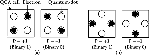
FIGURE 2.1 Basic QCA cells with two possible polarizations. (a) Regular cells. (b) Rotated cells. (I. Kong et al, Design of Goldschmidt Dividers with Quantum-Dot Cellular Automata, IEEE Transactions on Computers © 2013 IEEE.)
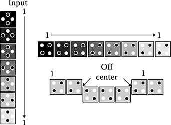
FIGURE 2.2 QCA wires. (S.-W. Kim and E. E. Swartzlander, Jr., Parallel Multipliers for Quantum-Dot Cellular Automata, IEEE Nanotechnology Materials and Devices Conference © 2009 IEEE.)
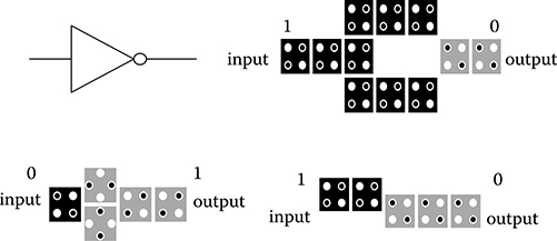
FIGURE 2.3 Various QCA inverters. (S.-W. Kim and E. E. Swartzlander, Jr., Parallel Multipliers for Quantum-Dot Cellular Automata, IEEE Nanotechnology Materials and Devices Conference © 2009 IEEE.)
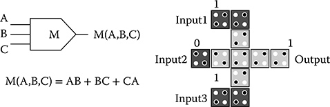
FIGURE 2.4 A QCA majority gate (S.-W. Kim and Earl E. Swartzlander, Jr., Parallel Multipliers for Quantum-Dot Cellular Automata, IEEE Nanotechnology Materials and Devices Conference © 2009 IEEE.)
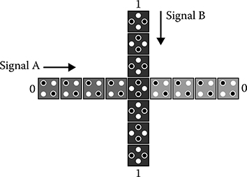
FIGURE 2.5 Coplanar “wire” crossing. (S.-W. Kim and E. E. Swartzlander, Jr., Multipliers with Coplanar Crossings for Quantum-Dot Cellular Automata, IEEE NANO © 2010 IEEE.)
In QCA, there are two types of crossings: coplanar crossings and multilayer crossovers. Coplanar crossings, such as the example shown in Figure 2.5, use only one layer but require regular and rotated cells. The two types of cells do not interact with each other when they are properly aligned, so they can be used for coplanar crossings. Published information suggests that coplanar crossings may be very sensitive to misalignment [4]. In a coplanar crossing, there is a possibility of a loose binding of the signal with the possibility of back-propagation from the far side. Preventing this requires more clock zones between the regular cells across the rotated cells.
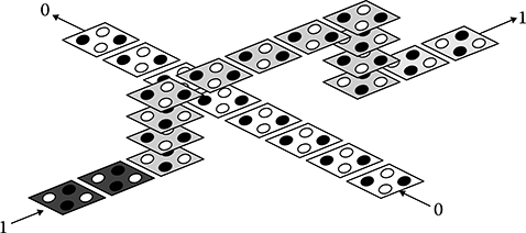
FIGURE 2.6 Multilayer “wire” crossover. (H. Cho and E. E. Swartzlander, Jr., Modular design of conditional sum adders using quantum-dot cellular automata, Proceedings 6th IEEE Conference on Nanotechnology © 2006 IEEE.)
An example of a multilayer crossover is shown in Figure 2.6. They use more than one layer of cells similar to the multiple metal layers in a conventional integrated circuit. The multilayer crossover is conceptually simple although there are questions about its realization, as it requires two overlapping active layers with vertical via connections. Previous work has examined the possibility of the multilayer QCA, but there has been no reported implementation yet [5]. Both types of crossovers are used in this chapter, multilayer for the adders and coplanar for the multipliers and divider.
2.2.2 QCA Clocking
With adiabatic switching accomplished by modulating the interdot tunneling barrier of the QCA cell, a multiple-phase clock is used in QCA. The cells are grouped together into pipelined zones [1,6,7]. This clocking scheme allows one zone of cells to perform a calculation and have its state held by raising its interdot barriers. The four clock phases shown in Figure 2.7 are used as switch, hold, release, and relax. During the switch phase, interdot potential barriers are lowered by applying an input signal, and data propagation occurs via electron tunneling. By gradually raising the barriers, the cells become polarized. For the hold phase the barriers are held high so the cell maintains its polarization and the output of the subarray can be used as inputs to the next stage. During the release and relax phases, the QCA cells start to lose their polarization by lowering the barriers and then they remain in an unpolarized state. This nature of clocking leads to inherent self-latching in QCA.
Generally, QCA circuits have very significant wiring delays. For a fast design in QCA, complexity constraints are very critical issues and the design needs to use architectural techniques to boost the speed considering these limitations.
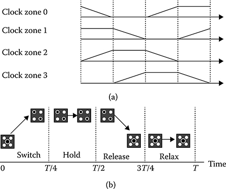
FIGURE 2.7 Four phase clocking scheme. (a) Clocking for a clock cycle with each lagging by 90°. (b) Interdot barriers in a clocking zone.
2.2.3 QCA Design Rules
The QCA cells are 18 nm by 18 nm with a 2 nm space on all four sides, with 5 nm diameter quantum dots. The cells are placed on a grid with a cell center-to-center distance of 20 nm. Because there are propagation delays between cell-to-cell reactions, there should be a limit on the maximum cell count in a clock zone. This insures proper propagation and reliable signal transmission. In this chapter, a maximum length of 16 cells is used. The minimum separation between two different signal wires is the width of two cells. Multilayer crossovers are used here for wire crossings. They use more than one layer of cells like a bridge. The multilayer crossover design is conceptually simple although there are questions about its realization, as it requires two overlapping active layers with vertical via connections. Alternatively, coplanar “crossovers” that may be easier to realize can be used with some modification to the basic designs. For circuit layout and functionality checking, a simulation tool for QCA circuits, QCADesigner, is used [8]. This tool allows users to do a custom layout and then verify QCA circuit functionality by simulations.
2.3 QCA Adders
Section 2.2.1 showed that interconnections incur significant complexity and wire delay when implemented with QCAs, so transistor circuit designs that assume wires have negligible complexity and delay need to be reexamined. In QCA, as the complexity increases, the delay may increase because of the increased cell counts and wire connections.
2.3.1 Carry-Flow Ripple Carry Adder*
In this subsection, the adder design is that of a conventional ripple carry adder, but with a FA whose layout is optimized for QCA technology [9]. The proposed adder design shows that a very low delay can be obtained with an optimized layout. To avoid confusion with conventional ripple carry adders, the new layout is referred to as the carry-flow ripple carry adder (CFA).
2.3.1.1 Basic Design Approach
Equations for a FA realized with majority gates and inverters are shown below. In a ripple carry adder most of the delays come from carry propagation. For faster calculation, reducing the carry propagation delay (i.e., carry-in to carry-out delay of a FA) is most important. The usual approach for fast carry propagation is to add additional logic elements. In this design, simplification is used instead.
si=aibici+aiˉbiˉci+ˉaibiˉci+ˉaiˉbici(2.1)
si=M(ˉM(ai,bi,ci),M(ai,bi,ˉci),ci)(2.2)
si=M(ˉci+1,M(ai,bi,ˉci),ci)(2.3)
ci+1=aibi+bici+aici(2.4)
ci+1=M(aibici)(2.5)
In QCA, the path from carry-in to carry-out only uses one majority gate. The majority gate always adds one more clock zone (one-quarter clock delay). Thus, each bit in the words to be added requires at least one clock zone, which sets the minimum delay.
2.3.1.2 Carry-Flow Full Adder Design
Figures 2.8a and 2.8b show the schematic and the layout of the carry-flow FA. The schematic and layout are optimized to minimize the delay and area. The carry propagation delay for 1 bit is a quarter clock and the delay from data inputs to the sum output is three-quarter clocks.
The wiring channels for the input/output synchronization should be minimized as wire channels add significantly to the circuit area. The carry-flow FA shown in Figure 2.8b requires only a one cell vertical offset between the carry-in and carry-out.
Figures 2.9 and 2.10 show 4- and 32-bit ripple carry adders, respectively, realized with carry-flow FAs. From the layouts, it is clear that for large adders, much of the area is devoted to skewing the input data and deskewing the outputs.
*Subsection 2.3.1 is based on [9].
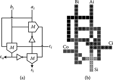
FIGURE 2.8 Carry-flow full adder. (a) Schematic. (b) Layout. (H. Cho and E. E. Swartzlander, Jr., Adder and multiplier design in quantum-dot cellular automata, IEEE Transactions on Computers © 2009 IEEE.)
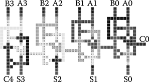
FIGURE 2.9 Layout of a 4-bit carry-flow adder. (H. Cho and E. E. Swartzlander, Jr., Adder and multiplier design in quantum-dot cellular automata, IEEE Transactions on Computers © 2009 IEEE.)
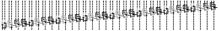
FIGURE 2.10 Layout of a 32-bit carry-flow adder. (H. Cho and E. E. Swartzlander, Jr., Adder and multiplier design in quantum-dot cellular automata, IEEE Transactions on Computers © 2009 IEEE.)
2.3.1.3 Simulation Results
The input and output waveforms for an 8-bit CFA are shown in Figure 2.11. For clarity, only 8-bit CFA simulation results are shown. The first meaningful output appears in the third clock period after 2.5 clock delays. First and last input/output pairs are highlighted.
2.3.2 Carry Lookahead Adder†
2.3.2.1 Architectural Design
The carry lookahead adder (CLA) has a regular structure. In CMOS implementations, it achieves high speed with a moderate complexity. For this section, 4-, 16-, and 64-bit CLA designs were developed following basic CMOS pipelined adder designs [10]. The pipelined designs avoid feedback signals (used in regular CMOS CLAs) that are difficult to implement with QCAs. Figures 2.12 through 2.14 show block diagrams of the designs for 4-, 16-, and 64-bit CLAs, respectively. The designs use 4-bit slices for the lookahead logic, so each factor of 4 increase in word size requires an additional level of lookahead logic.
The PG block has a generate output, gi = aibi, which indicates that a carry is “generated” at bit position i, and a propagate output pi = ai + bi, which indicates that a carry entering bit position i will “propagate” to the next bit position. They are used to produce all the carries in parallel at the successive blocks. The block PG section produces and transfers block generate/propagate signals to the next higher level. The CLA and block CLA sections are virtually identical except for the different hierarchy of their positions and additional bypassing signals. Their outputs and PG outputs are used to calculate the final sum at each bit position. Because of the pipeline design, all sum signals are available at the same clock period.
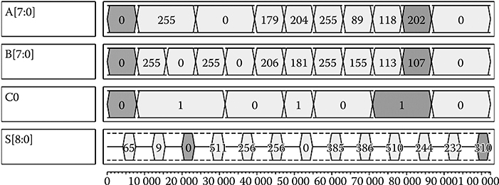
FIGURE 2.11 Simulation results for 8-bit carry-flow adder. (H. Cho and E. E. Swartzlander, Jr., Adder and multiplier design in quantum-dot cellular automata, IEEE Transactions on Computers © 2009 IEEE.)
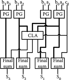
FIGURE 2.12 4-bit carry lookahead adder block diagram. (H. Cho and E. E. Swartzlander, Jr., Adder designs and analyses for quantum-dot cellular automata, IEEE Transactions on Nanotechnology © 2007 IEEE.)
†Subsection 2.3.2 is based on [11].
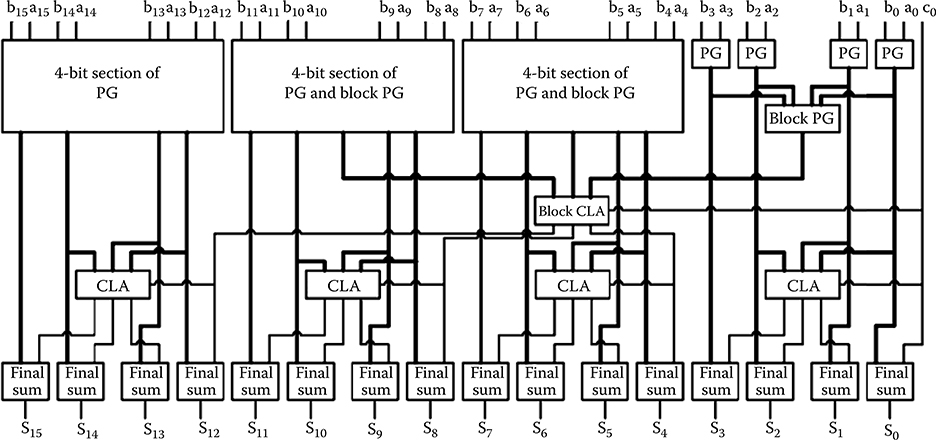
FIGURE 2.13 16-bit carry lookahead adder block diagram. (H. Cho and E. E. Swartzlander, Jr., Adder designs and analyses for quantum-dot cellular automata, IEEE Transactions on Nanotechnology © 2007 IEEE.)
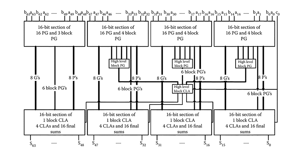
FIGURE 2.14 64-bit carry lookahead adder block diagram. (H. Cho and E. E. Swartzlander, Jr., Adder designs and analyses for quantum-dot cellular automata, IEEE Transactions on Nanotechnology © 2007 IEEE.)
2.3.2.2 Schematic Design
Using the block PG equations, AND/OR logic functions are mapped to majority gates to build the 4-bit section of PG and block PG. The CLA and block CLA sections are described by the following equations:
pb+pi+3pi+2pi+1pi(2.6)
gb=gi+3+pi+3gi+2+pi+3pi+2gi+1+pi+3pi+2pi+1gi(2.7)
ci+1=gi+pici(2.8)
ci+2=gi+1+pi+1gi+pi+1pici(2.9)
ci+3=gi+2+pi+2gi+1+pi+2pi+1gi+pi+2pi+1pici(2.10)
Because of the characteristics of majority gates in QCA, a half adder and a FA have the same complexity. The FA design shown in Figure 2.8 uses three majority gates. An exclusive OR gate (equivalent to a half adder) also needs three majority gates. Thus, both adders have the same complexity ignoring the wire routing complexity.
The final sum adder is similar to a FA except that the inputs are pi, gi, and ci rather than ai, bi, and ci. Using these inputs, wire routing is simplified.
After the optimization, the final sum adder is implemented with three majority gates. Figure 2.15 shows the gate level diagram of the given final sum adder equation.
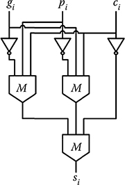
FIGURE 2.15 Final sum adder schematic. (H. Cho and E. E. Swartzlander, Jr., Adder designs and analyses for quantum-dot cellular automata, IEEE Transactions on Nanotechnology © 2007 IEEE.)
si=pigici+piˉgiˉci+ˉpigiˉci+ˉpiˉgici(2.11)
si=M(ˉM(ˉpigici),ˉM(piˉgici)ˉci)(2.12)
2.3.2.3 Layout Design
Figures 2.16 and 2.17 show the layouts of 4- and 16-bit CLAs from QCADesigner.
2.3.2.4 Simulation Results
With QCADesigner version 2.0.3, the circuit functionality of the CLA is verified. The following parameters are used for a bistable approximation: cell size = 20 nm, number of samples = 102,400, convergence tolerance = 0.00001, radius of effect = 41 nm, relative permittivity = 12.9, clock high = 9.8e−22J, clock low = 3.8e−23J, clock amplitude factor = 2, layer separation = 11.5 nm, maximum iterations per sample = 10,000 [8].
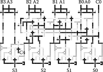
FIGURE 2.16 4-bit carry lookahead adder layout. (H. Cho and E. E. Swartzlander, Jr., Adder designs and analyses for quantum-dot cellular automata, IEEE Transactions on Nanotechnology © 2007 IEEE.)
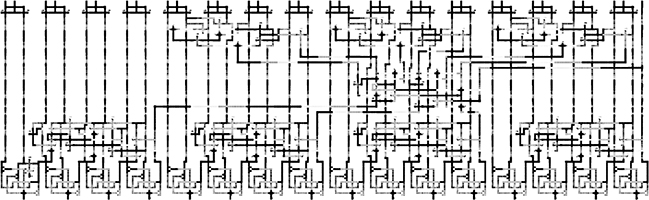
FIGURE 2.17 16-bit carry lookahead adder layout. (H. Cho and E. E. Swartzlander, Jr., Adder designs and analyses for quantum-dot cellular automata, IEEE Transactions on Nanotechnology © 2007 IEEE.)
For clarity, only the 4-bit CLA simulation results are shown. The input and output waveforms are shown in Figure 2.18. The first meaningful output appears in the fourth clock tick after 3.5 clock delays. The first and last input/output pairs are highlighted.
2.3.3 Conditional Sum Adder‡
2.3.3.1 Architectural Design
In CMOS, the CSA is frequently used when the highest speed is required. CSAs of 4, 8, 16, 32, and 64 bits were designed and simulated [12]. The structures are based on the recursive relations shown in Figure 2.19.
This design can be divided into two half-size calculations. The upper half calculation is duplicated (one assuming a carry-in of 0 and one assuming a carry-in of 1). The carry output from the lower half is used to select the correct upper half output. This process is continued recursively down to the bit level.
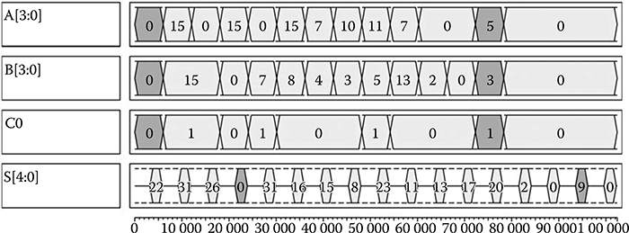
FIGURE 2.18 Simulation results for 4-bit CLA using QCADesigner version 2.0.3. (H. Cho and E. E. Swartzlander, Jr., Adder designs and analyses for quantum-dot cellular automata, IEEE Transactions on Nanotechnology © 2007 IEEE.)
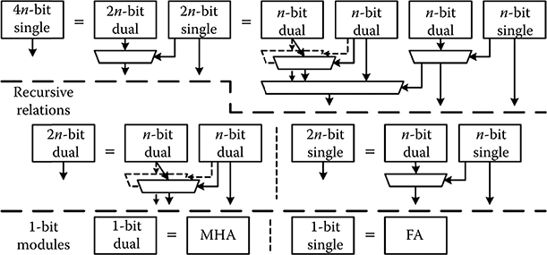
FIGURE 2.19 Recursive structure of a conditional sum adder. (H. Cho and E. E. Swartzlander, Jr., Modular design of conditional sum adders using quantum-dot cellular automata, Proceedings 6th IEEE Conference on Nanotechnology © 2006 IEEE.)
‡Subsection 2.3.3 is based on [12].
These recursive relations produce modular designs. Figure 2.20 shows the block diagram of an 8-bit CSA. The blocks just below the modified half adders (MHAs) are referred to as level 1. Successive lower blocks are called level 2, 3, and so on.
2.3.3.2 Schematic Design
The following equations are used for CSAs. ai and bi denote inputs at bit position i. si represents the sum output at bit position i and ci+1 represents the carry output gener ated from bit position i. Spi means the sum of bit position when the carry input value is p and cqi+1 means the carry output of bit position i when the carry input is q. At bit position i, the definitions of sum and carry output are s0i=ai⊕bi,s1i=aiˉ⊕bi=¯ai⊕bi, c0i+1=aibi and c1i+1=ai+bi.
s0=a0⊕b0⊕c0(2.13)
c1=M(a0b0c0)(2.14)
s1=s01ˉc1+s11c1(2.15)
c2=c02ˉc1+c12c1(2.16)
si=s0iˉci+s1ici(2.17)
ci+1=c0i+1ˉci+c1i+1ci(2.18)
As shown in Figure 2.20, the circuits are composed of a FA, MHAs, and multiplexers. The schematics of the MHA circuits are shown in Figure 2.21. Figure 2.21a and b shows two options for half-adder modules. In transistor circuits, the duplicated half adder (DHA) has the same delay and more area than the MHA.
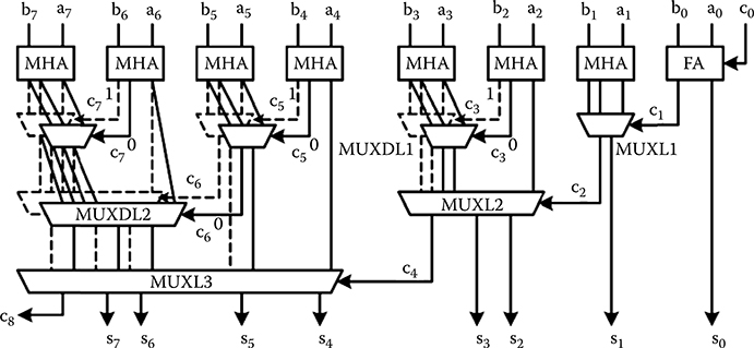
FIGURE 2.20 8-bit conditional sum adder block diagram. (H. Cho and E. E. Swartzlander, Jr., Modular design of conditional sum adders using quantum-dot cellular automata, Proceedings 6th IEEE Conference on Nanotechnology © 2006 IEEE.)
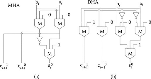
FIGURE 2.21 Half adder schematics. (a) Modified half adder. (b) Duplicated half adder. (H. Cho and E. E. Swartzlander, Jr., Modular design of conditional sum adders using quantum-dot cellular automata, Proceedings 6th IEEE Conference on Nanotechnology © 2006 IEEE.)
In QCA, the area of the DHA is still large but the delay is slightly less than that of the MHA by one-quarter of a clock. This trade-off governs the circuit choice. The general MHA module for CSA has four outputs, but QCA design only has three outputs. The sum for a carry-in of one is the complement of the sum for a carry-in of zero. The inverter is realized at the destination, which eliminates a wire. Thus, two-wire channels are reduced to one.
The required multiplexers are similar to transistor circuits. The inverters for complementing the sums are implemented just before the multiplexers. Successive levels of multiplexers are implemented in the same manner.
2.3.3.3 Layout Design
Figure 2.22a and b shows the layouts for the two types of half adder modules. A DHA module has larger area and more cells, but it has more delay margin. This shows a difference from transistor circuits. DHA modules are used in the implementations for the timing margin. The width of the design is dominated by the multiplexers. The heights of the MHA and the DHA are the same. The only disadvantage of DHA is a small increase in the number of cells used, but this is negligible for large adders.
The layouts for 4- and 16-bit CSAs are shown in Figures 2.23 and 2.24.
2.3.4 Comparison of the QCA Adders
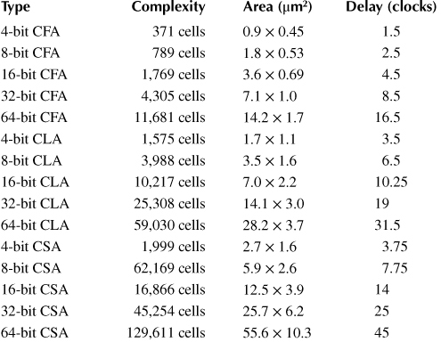
Table 2.1 compares the 4-, 8-, 16-, 32-, and 64-bit CFAs, CLAs, and CSAs. The areas reported in Table 2.1 are the size of the bounding box (i.e., the smallest rectangle that contains the layout). As the design of the CSA is roughly triangular in shape, the size can be reduced by approximately 25% if the unused areas are taken into account, but it will still be the largest of the three types of adders.
From the values shown in Table 2.1, the cell counts for an adder with n-bit operands are roughly O(n1.21) for CFAs, O(n1.32) for CLAs, and O(n1.5) for CSAs. Areas are O(n1.42) for CLAs, O(n1.47) for CLAs, and O(n1.73) for CSAs. Delays are n+0.5 for RCAs, O(n0.8) for CLAs, and O(n0.91) for CSAs. These results show that the design overheads are indeed significant.
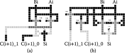
FIGURE 2.22 Half adder layouts. (a) Modified half adder. (b) Duplicated half adder. (H. Cho and E. E. Swartzlander, Jr., Modular design of conditional sum adders using quantum-dot cellular automata, Proceedings 6th IEEE Conference on Nanotechnology) © 2006 IEEE.)
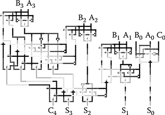
FIGURE 2.23 4-bit conditional sum adder layout. (H. Cho and E. E. Swartzlander, Jr., Modular design of conditional sum adders using quantum-dot cellular automata, Proceedings 6th IEEE Conference on Nanotechnology © 2006 IEEE.)
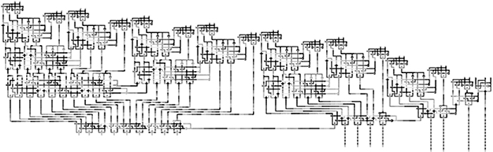
FIGURE 2.24 16-bit conditional sum adder layout. (H. Cho and E. E. Swartzlander, Jr., Modular design of conditional sum adders using quantum-dot cellular automata, Proceedings 6th IEEE Conference on Nanotechnology © 2006 IEEE.)
The CFA is the best design in QCA. The complexity is significantly lower than that of the CLA or the CSA. Also, rather surprisingly, the delay is less, even for large adders.
The delays of the CLAs are less than that of the CSAs. Comparing QCA circuits with CMOS circuits, the main differences are observed in the CSAs. In transistor circuits, the CSA shows similar speed to the CLA, even though the size of the CSA is larger than that of the CLA. But in QCA, the CSA is slower and the complexity and area are much greater than that of the CLA.
Table 2.1 Adder Comparisons with Multilayer Crossovers
2.4 QCA Multipliers
This chapter explores the implementation of two types of parallel multipliers in QCA technology. Array multipliers that are well suited to QCA are constructed and formed by a regular lattice of identical functional units so that the structure is conformable to QCA technology without extra wire delay are considered in Section 2.4.2. Column compression multipliers, such as Wallace multipliers are implemented with several different operand sizes in Section 2.4.3.3. Section 2.4.4 gives a summary of multiplier design in QCA.
2.4.1 Introduction
Figure 2.25 shows the multiplication of two n-bit unsigned binary numbers that yields a 2n-bit product. The basic equation is as follows:
P=A×B(2.19)
P=n−1∑j=0aj2j×n−1∑i=0bi2i(2.20)
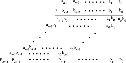
FIGURE 2.25 Multiplication of two n-bit binary numbers.
P=2n−1∑k=0pk2k(2.21)
where the multiplicand is A (= an−1,…, a0), the multiplier B (= bn−1,…, b0), and the product P (= p2n−1,…, pn−1,…, p0).
2.4.2 QCA Array Multipliers§
Array multipliers that are well suited to QCA are studied and analyzed in this section. An array multiplier is formed by a regular lattice of identical functional units so that the structure conforms to QCA technology without extra wire delay.
2.4.2.1 Schematic Design
A 4-bit by 4-bit array multiplier is shown in Figure 2.26. It has 5 rows and an irregular lattice [13]. The 4-bit by 4-bit array multiplier consists of 16 AND gates, 3 half adders, and 9 FAs. The carry outputs from each FA go to the next row. One operand propagates from left to right in the array multiplier. In general, the array multipliers have a latency of 4N − 2. Table 2.2 shows the required hardware for the array multipliers.
2.4.2.2 Implementation of Array Multipliers with QCAs
The 4-bit by 4-bit array multiplier is implemented as shown in Figure 2.27. It can be extended to make a larger 8-bit by 8-bit multiplier as shown in Figure 2.28. The area of the array multiplier gets 4.35 times larger as the operand size is doubled because of its irregular lattice and one more last row.
2.4.3 Wallace Multipliers for QCA**
2.4.3.1 Introduction
The Wallace strategy for fast multiplication is to form the N by N array of partial product bits, then reduce them to a two-row matrix with an equivalent numerical value, and then to add the two rows with a carry propagating adder [15]. To handle the reduction stage, Wallace’s strategy is to combine partial product bits with the use of full and half adders at the earliest opportunity. Figure 2.29 shows a dot diagram of a 4-bit by 4-bit Wallace multiplier that has two reduction stages. A dot indicates a partial product of the multiplication. Plain and crossed diagonal lines indicate the outputs of a FA and a half adder, respectively. The block diagram of a 4-bit by 4-bit Wallace multiplier is shown in Figure 2.30.
§Subsection 2.4.2 is based on [13].
**Subsection 2.4.3 is based on [14].
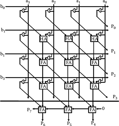
FIGURE 2.26 Schematic of an array multiplier. (S.-W. Kim and E. E. Swartzlander, Jr., Multipliers with Coplanar Crossings for Quantum-Dot Cellular Automata, IEEE NANO © 2010 IEEE.)
Table 2.2 Required Components for Array Multipliers
Type |
Full Adders |
Half Adders |
AND Gates |
Array: 4-bit by 4-bit |
9 |
3 |
16 |
Array: 8-bit by 8-bit |
49 |
7 |
64 |
Array: N-bit by N-bit |
(N – 1)2 |
N – 1 |
N2 |
FIGURE 2.27 Layout of a 4-bit by 4-bit array multiplier. (S.-W. Kim and E. E. Swartzlander, Jr., Multipliers with Coplanar Crossings for Quantum-Dot Cellular Automata, IEEE NANO © 2010 IEEE.)
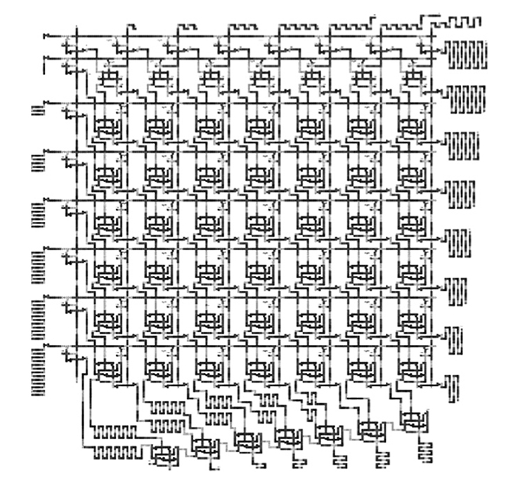
FIGURE 2.28 Layout of an 8-bit by 8-bit array multiplier. (S.-W. Kim and E. E. Swartzlander, Jr., Multipliers with Coplanar Crossings for Quantum-Dot Cellular Automata, IEEE NANO © 2010 IEEE.)
2.4.3.2 Schematic Design
In each stage of the reduction, the Wallace multiplier conducts a preliminary grouping of rows into sets of three. Within each three-row set, FAs and half adders are used to reduce the three rows to two. Rows that are not part of a three-row set are transferred to the next stage without modification. The bits of these rows are considered in the later stages. An 8-bit by 8-bit Wallace multiplier has four reduction stages and intermediate matrix heights of 2, 3, 4, and 6. A dot diagram of an 8-bit by 8-bit Wallace multiplier is shown in Figure 2.31. Table 2.3 shows the required hardware.
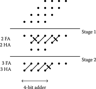
FIGURE 2.29 Dot diagram of a 4-bit by 4-bit Wallace reductions. (S.-W. Kim and E. E. Swartzlander, Jr., Parallel Multipliers for Quantum-Dot Cellular Automata, IEEE Nano technology Materials and Devices Conference © 2009 IEEE.)
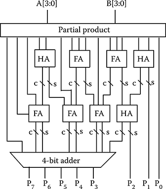
FIGURE 2.30 Block diagram of a 4-bit by 4-bit Wallace multiplier. (S.-W. Kim and E. E. Swartzlander, Jr., Parallel Multipliers for Quantum-Dot Cellular Automata, IEEE Nanotechnology Materials and Devices Conference © 2009 IEEE.)
2.4.3.3 Implementation of Wallace Multipliers with QCAs
The layout of a 4-bit by 4-bit Wallace multiplier is shown in Figure 2.32. In these multipliers stair-like ripple carry adders are used for synchronization and to make each stage pipelined. A total of 3295 cells are used to make 4-bit by 4-bit Wallace multiplier with an area of 7.39 μm2 [14]. An 8-bit by 8-bit Wallace multiplier is shown in Figure 2.33. The 8-bit by 8-bit multiplier has about 10 times as many cells as the 4-bit by 4-bit multiplier.
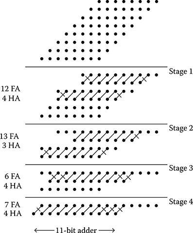
FIGURE 2.31 Dot diagram of 8-bit by 8-bit Wallace multiplier. (S.-W. Kim and E. E. Swartzlander, Jr., Multipliers with Coplanar Crossings for Quantum-Dot Cellular Automata, IEEE NANO © 2010 IEEE.)
Table 2.3 Required Adders for Wallace Multipliers
Type |
Full Adders |
Half Adders |
Final Adder Size |
Wallace: 4-bit by 4-bit |
5 |
3 |
4 |
Wallace: 8-bit by 8-bit |
38 |
15 |
11 |
2.4.3.4 Simulation Results
Simulations were done with QCADesigner [8] assuming coplanar wire “crossings” and a maximum of 15 cells per clock zone. The size of the basic quantum cell was set at 18 nm by 18 nm with 5-nm diameter quantum dots. The center-to-center distance is set at 20 nm for adjacent cells. The following parameters are used for a bistable approximation: 51,200 samples, 0.001 convergence tolerance, 65-nm radius effect, 12.9 relative permittivity, 9.8e−22J clock high, 3.8e−23J clock low, 2-clock amplitude factor, 11.5 layer separation, 100 maximum iterations per sample.
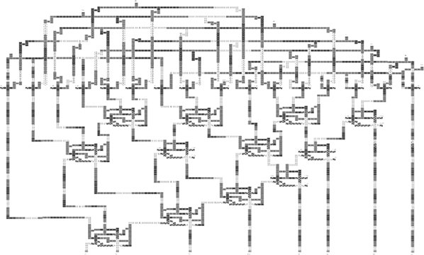
FIGURE 2.32 Layout of a 4-bit by 4-bit Wallace multiplier. (S.-W. Kim and E. E. Swartzlander, Jr., Parallel Multipliers for Quantum-Dot Cellular Automata, IEEE Nanotechnology Materials and Devices Conference © 2009 IEEE.)
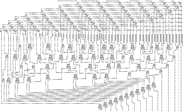
FIGURE 2.33 Layout of an 8-bit by 8-bit Wallace multiplier. (S.-W. Kim and E. E. Swartzlander, Jr., Multipliers with Coplanar Crossings for Quantum-Dot Cellular Automata, IEEE NANO © 2010 IEEE.)
The 4-bit by 4-bit Wallace multiplier has 10-clock latency, and 3295 cells with area that is comparable to the array multiplier. The 8-bit by 8-bit Wallace multiplier has more than 4 times the latency and 11 times the area of the 4-bit by 4-bit multiplier. These results show that simple and dense structures are needed. In addition, if they can be realized, multilayer wire crossings might mitigate the wire burden.
2.4.4 Comparison of QCA Multipliers
Table 2.4 shows a comparison of the simulation results for 4 by 4 and 8 by 8 bit array and Wallace multipliers. The various 4-bit by 4-bit multipliers have 10- to 14-clock latency, and 3295–3738 cells. The 8-bit by 8-bit multipliers have roughly 2 to 3 times the latency and 4 to 8 times the cell count of the 4-bit by 4-bit multipliers. The 8-bit by 8-bit multipliers are much slower and larger than would be expected from CMOS multipliers, where the Wallace multiplier latency scales as the logarithm of the operand size. These results show that the most significant factor in the performance is the wiring. At least part of the explanation for this is that many of the wires are quite long. The long wires significantly affect the timing, 33.8% of the latency is due to the wiring.
Thus it seems that array multipliers are the best choice for QCA implementation. The latency is least (for all but the smallest multipliers) and the area is much less than Wallace multipliers.
2.5 QCA Goldschmidt Divider
Convergent dividers where an initial estimate of the quotient in refined iteratively are used where high speed is required and when one or more multipliers are available. Section 2.5.3 presents the design of a Goldschmidt convergent divider in QCA [16].
With CMOS, large iterative computational circuits such as convergent dividers are often built with state machines to control the various computational elements. Because of QCA wire delays, state machines have problems due to long delays between the state machine and the units to be controlled. Even a simple 4-bit microprocessor that has been implemented with QCA [16] was done without using a state machine. Because of the difficulty of designing sequential circuits, there has been little research into using QCAs to realize large iterative computational units.
This section presents a design for a convergent divider using the Goldschmidt algorithm implemented with a data tag architecture to solve the difficulty in designing iterative computation units. In Section 2.5.1, the Goldschmidt iterative division algorithm is described. In Section 2.5.2, the data tag method is presented. In Section 2.5.3, an implementation of the Goldschmidt divider using the proposed method is reviewed in detail. Finally, simulation results are presented in Section 2.5.4.
Table 2.4 Comparison of QCA Multipliers
Type |
Cell Count |
Area (μm2) |
Latency |
Array: 4-bit by 4-bit |
3,738 |
6.02 |
14 |
Array: 8-bit by 8-bit |
15,106 |
21.5 |
30 |
Wallace: 4-bit by 4-bit |
3,295 |
7.39 |
10 |
Wallace: 8-bit by 8-bit |
26,499 |
82.2 |
36 |
2.5.1 Goldschmidt Division Algorithm††
In Goldschmidt division [17,18], an approximate quotient converges toward the true quotient by multiple iterations. The division operation can be viewed as the manipulation of a fraction. The numerator (N) and the denominator (D) are each multiplied by a sequence of numbers so that the value of D approaches 1 and the value of N approaches the quotient. In the first step, both N and D are multiplied by F0, an approximation to the reciprocal of D. Often F0 is produced by a reciprocal table with very limited precision, thus, the product of D times F0 is not exact, but has an error, ∊. Therefore, the first approximation of the quotient is as follows:
Q=N×F0D×F0=N0D0=N01−ε(2.22)
At the next iteration, N0 and D0 are multiplied by F1, which is given by:
F1=(2−D0)=2−(1−ε)=1+ε(2.23)
Note that often the one’s complement of Di is used for Fi+1 as that avoids the need to do a subtraction. The result is a slight (1 least significant bit [LSB]) increase in the error, which very slightly reduces the rate of convergence.
Q=N0×F1D0×F1=N0(1+ε)(1−ε)(1+ε)=N0(1+ε)(1−ε2)=N1D1(2.24)
At the i+1-st iteration, Fi is as follows:
Fi=(2−Di−1)=1+ε2i−1fori>0(2.25)
Q=NiDi=Ni−1FiDi−1Fi=Ni−1(1+ε2i−1)(1−ε2i)(2.26)
As the iterations continue, Ni converges toward Q with quadratic precision, which means that the number of correct digits doubles on each iteration.
To show the Goldschmidt division, consider the following example: Q = 0.6/0.75. From a look-up table, the approximate reciprocal of D (i.e., 0.75) is F0 = 1.3:
Q=N×F0D×F0=0.6×1.30.75×1.3=0.780.975=N0D0(2.27)
Then F1 = 2 – D0 = 2 – 0.975 = 1.025:
Q=N0×F1D0×F1=0.78×1.0250.975×1.025=0.79950.999375=N1D1(2.28)
Then F2 = 2 – D1 = 2 – 0.999375 = 1.000625:
Q=N1×F2D1×F2=0.7995×1.0006250.999375×1.000625=0.7999996850.999999609395=N2D2(2.29)
††Subsection 2.5.1 is based on [19,20].
The errors between N0, N1, and N2 are 0.02, 0.0005, and 0.0000003125, respectively. This shows that the value of Ni converges quadratically to the value of Q.
2.5.2 Data Tag Method
To resolve the problem of communication commands from state machines to the computational units, a data tag method is used as shown in Figure 2.34. In this method, data tags travel with the data, and local tag decoders (TD in the Figure 2.34) generate control signals for the computational circuits (i.e., COMP1, COMP2). The tags travel with the data through the same number of pipeline stages as the corresponding computational circuits, and local tag decoders generate control signals appropriate to each datum. As the tags travel with the data and local tag decoders produce the control signals for the units, the synchronization issues that are a problem in state machines are significantly mitigated. In QCAs, the data tag method can be implemented very efficiently as the delays to keep the data tags synchronized to the data are generated inherently via the gates and wires in the QCAs.
An advantage of the data tag architecture is that each datum on a data path can be processed differently according to the tag information. For example, in typical Goldschmidt dividers controlled by a state machine, a new division cannot be started until the previous division is completed. There are many pipeline stages in QCA computational circuits, and most stages may be idle during iterations. With the data tag method, each datum on a data path can be processed by the operation that is required at that stage. As divisions at different stages are processed in a time-skewed manner, new divisions can be started while previous divisions are in progress as long as the initial pipeline stage of the data path is free. As a result, the throughput can be increased to a level that is much greater than that which is implied by the latency.
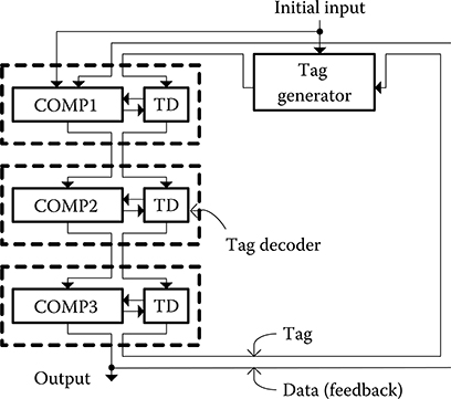
FIGURE 2.34 Computation unit implementation using data tags. (I. Kong et al., Design of a Goldschmidt iterative divider for quantum-dot cellular automata, IEEE/ACM International Symposium on Nanoscale Architectures © 2009 IEEE.)
A 12-bit Goldschmidt divider has been designed using the data tag method. The flowchart is shown in Figure 2.35. The divider uses a low-precision ROM that gives 4-bit values for F0. The divider performs three iterations, the first with a value from the ROM followed by two iterations with the one’s complement of Di for Fi+1.
The flowchart realizes the steps from Section 2.5.1. To start a new division, the tag generator issues a new tag (DT = 1) for the data. On the first iteration, the factor is obtained from the ROM and used to multiply the denominator and numerator. For the second and third iterations, the factor is obtained by inverting the current value of the denominator. After the third iteration, the value of the numerator is output as the quotient. The local tag decoders control the multiplexers according to the tag associated with the data. Once a division has started, it progresses through the required iterations, irrespective of any other divisions that are being performed.
2.5.3 Implementation of the Goldschmidt Divider
The Goldschmidt divider was designed using coplanar wire crossings with the design guidelines suggested by K. Kim et al. [21,22]. Coplanar wire crossings are used for this research, as a physical implementation of multilayer crossovers has not been demonstrated yet. If multilayer crossovers become available, the design will be slightly smaller and faster. The design guidelines [21] are kept except for the limitation on majority gate outputs. Robust operation of majority gates is attained by limiting the maximum number of cells that are driven by each output, which is verified using the coherence vector method. The maximum cell count for each circuit component in a clock zone is determined by simulations with sneak noise sources. For this work, the maximum length of a simple wire is 14 cells and the minimum length is 2 cells. As a result, each majority gate drives a line that is at least two cells long to insure proper operation.
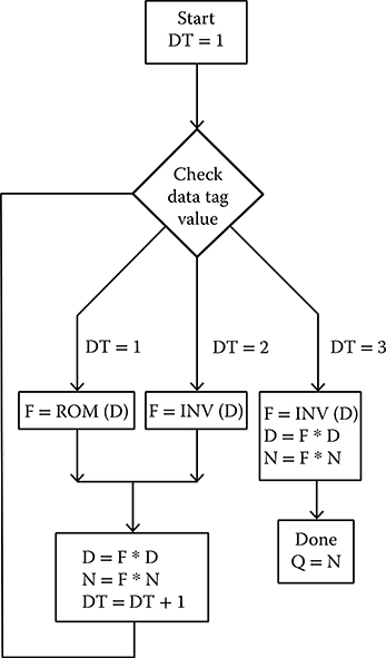
FIGURE 2.35 Flow chart of the 12-bit Goldschmidt divider using data tags.
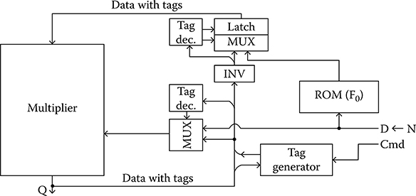
FIGURE 2.36 Block diagram of the Goldschmidt divider using the data tag method. (I. Kong et al., Design of a Goldschmidt iterative divider for quantum-dot cellular automata, IEEE/ACM International Symposium on Nanoscale Architectures © 2009 IEEE.)
A block diagram of the divider is shown in Figure 2.36. The main elements are the ROM and the multiplier. In addition, there are the tag generator, tag decoders, a word-wide inverter, and a few multiplexers. The CMD signal is asserted together with D, and a new tag is generated from the tag generator. Then N is entered. The tag decoders control the multiplexers and the latches using the tag that is associated with D. During the first iteration (used to normalize the denominator to a value that is close to 1), the multiplexers are set so that D and N are multiplied sequentially by F0 from the reciprocal ROM. After the first denominator normalization step is completed, the tag is incremented by the tag generator. During the subsequent iterations, the multiplexers select D or N from the outputs of the multiplier and Fi that is computed by inverting the bits of D (as noted in Section 2.5.1; this one’s complement operation approximates 2 – D with an error of 1 LSB). After three or four iterations, the final values of D and N have been computed, so N (the approximate value of Q) is output and the tag generator eliminates the tag.
2.5.3.1 23 by 3-Bit ROM Table
The 23 by 3-bit reciprocal ROM consists of a 3-bit decoder and an 8 by 3 ROM array as shown in Figure 2.37. All the ROM cells have the same access time, 7 clocks. The data are programmed by setting one input of the OR gate inside each ROM cell. Both the 12-bit and the 24-bit dividers use the same ROM. As the range of Di[0:11] is 0.5 ≤ D < 1 for the Goldschmidt division, Di[0:1] are always 01, so Di[2:4] is used as the input to the 3-bit ROM. Similarly, the ROM output is F0[1:3] as F0[0] is always 1. Thus, an 8 by 3 ROM implements a 32-word by 4-bit table.
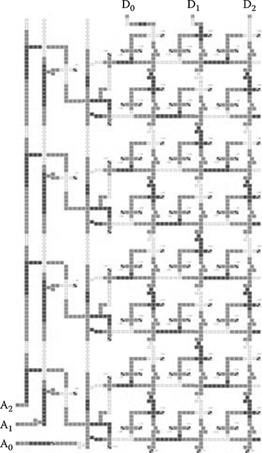
FIGURE 2.37 Layout of the 8-word by 3-bit reciprocal ROM. (I. Kong et al., Design of a Goldschmidt iterative divider for quantum-dot cellular automata, IEEE/ACM International Symposium on Nanoscale Architectures © 2009 IEEE.)
2.5.3.2 Array Multiplier
The divider uses a 12-bit by 12-bit array multiplier as array multipliers are attractive for QCA as shown in Section 2.4. The basic cell of the multiplier is a FA implemented with three majority gates. The cell has signal delays of 1 clock for the carry output, 2 clocks for the sum, and an area of 20 by 29 cells. The 12-bit by 12-bit multiplier has two inputs, A[11:0] and B[11:0], and a most significant output, M[11:0]. The latency of an N-bit by N-bit array multiplier is 4N – 2, so the multiplier latency of 46 is the largest component of the latency to perform an iteration. The unused least significant outputs are not left unconnected as that would violate the QCA design guidelines. Additional dummy cells are attached to the unused outputs for robust transfers of the signals.
To realize Goldschmidt dividers of other sizes, much of the design remains the same as for the 12-bit divider. The multiplier size is changed to match the divider word size. If the ROM for F0 is kept as 8 words of 3 bits, the number of iterations will change. If the ROM size is increased to 32 words of 5 bits, one fewer iteration is needed. The larger ROM may have slightly larger latency, but as one iteration (that includes a pair of high-latency multiplications) is saved, the total divider latency is reduced.
2.5.4 Simulation Results
The layout of the 12-bit Goldschmidt divider is shown in Figure 2.38. The design has been implemented and simulated using QCADesigner version 2.0.3 [8]. Most default parameters for bistable approximation in QCADesigner version 2.0.3 are used except two parameters: the number of samples and the clock amplitude factor. As the recommended number of samples is 1000 times the number of clocks in a test vector, the number of samples is determined to be 226,000. Because adiabatic switching is effective to prevent a QCA system from relaxing to a wrong ground state [1], the clock amplitude factor is adjusted to 1.0 for more adiabatic switching. Other major parameters are as follows: size of QCA cell = 18 nm by 18 nm, center-to-center distance = 20 nm, radius of effect = 65 nm, and relative permittivity = 12.9.
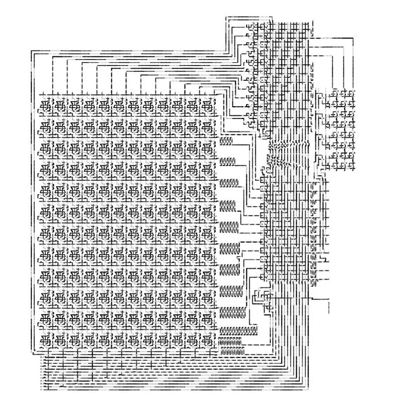
FIGURE 2.38 Layout of the 12-bit Goldschmidt divider. (I. Kong et al., Design of a Goldschmidt iterative divider for quantum-dot cellular automata, IEEE/ACM International Symposium on Nanoscale Architectures © 2009 IEEE.)
The area for the 12-bit Goldschmidt divider is 89.8 μm2 (8.8 μm × 10.2 μm), and the total number of QCA cells is 55,562. The delays of the functional units are shown in Table 2.5. As a division requires three iterations, the total latency for a single isolated division is 219 clocks. Although this latency (in terms of the number of clocks) seems quite high, the clock rate for semiconductor QCA is on the order of 1 THz, so the time per isolated division can be less than 1/4 ns. Given the two clocks (one for D and the second for N) with a latency of 73 clocks per iteration, as many as 35 divisions can be started while the first one is progressing. Then successive quotients are available on every other clock.
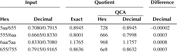
The 12-bit Goldschmidt divider was tested using bottom-up verification as a full simulation for a case takes about 7 hours. Each unit block is verified exhaustively, and then the full integration is tested. A simulation of four consecutive divisions is shown in Figure 2.39. The first division computes 0.7080/0.7915. The inputs D = 0.65516 and N = 0.5aa16 are shown at the left side of the second row of Figure 2.24a. The results for this division (Q = 0.894510) are shown starting at clock 218 (sequence da16) on the second row of Figure 2.28b, D = 0.7ff16 and Q = N = 0.72816. Three additional divisions are performed immediately after the first division to show that pipe-lining achieves a peak division throughput of one division for every two clock cycles.
Table 2.6 shows the results for the four example divisions. The first two columns give the numerator and denominator in hexadecimal and decimal, respectively. Column 3 gives the exact quotient. Columns 4 and 5 give the result computed by the Goldschmidt divider in hexadecimal and decimal. Finally, the last column gives the difference between the exact and the computed (QCA) quotients. In all four cases the computed quotients are accurate to within about 1 LSB.
2.6 Conclusion
A Goldschmidt divider (an iterative computational circuit) for QCA is implemented efficiently in a new architecture using data tags. The proposed data tag method avoids the synchronization problems that arise with conventional state machines in QCA because of the long delays between the state machines and the units to be controlled. In the proposed architecture, it is possible to start a new division at any iteration stage of a previous issued operation. As a result, the throughput is significantly increased because multiple division computations can be performed in a time-skewed manner using one iterative divider.
Table 2.5 Delays of the Functional Units
Functional Unit |
Delay (Clocks) |
Tag generator |
3 |
Multiplexer and tag decoder |
19 |
8 by 3 ROM |
7 |
12-Bit array multiplier |
46 |
Data bus |
5 |
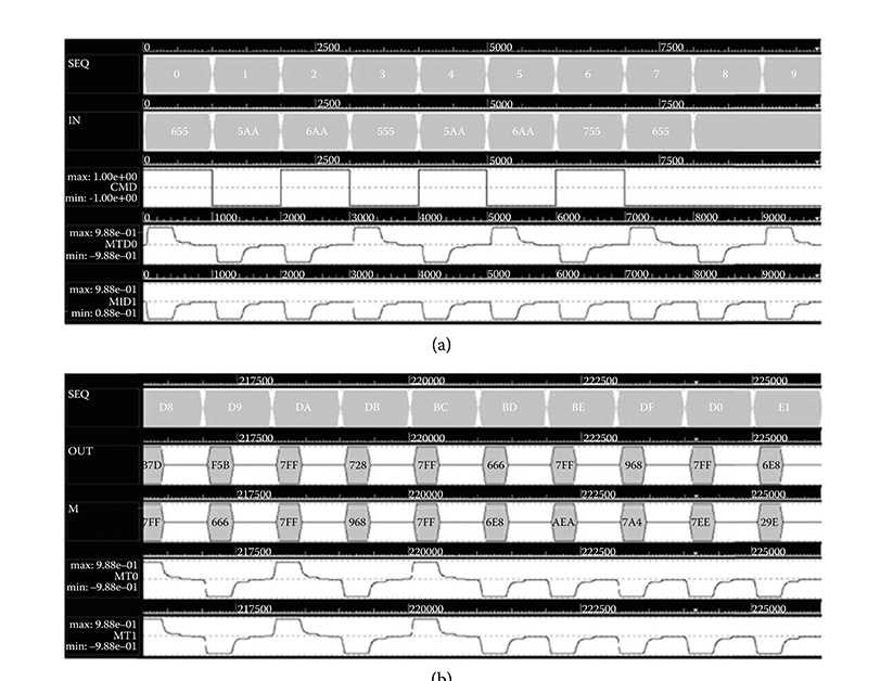
FIGURE 2.39 Simulation results. (a) Input vectors for four consecutive divisions. (b) Output waveforms for the four quotients. (I. Kong et al., Design of Goldschmidt dividers with quantum-dot cellular automata, IEEE Transactions on Computers © 2013 IEEE.)
Table 2.6 Example Divisions
References
1. C. Lent and P. Tougaw, A device architecture for computing with quantum dots, Proceedings of the IEEE, 85, 541–557, 1997.
2. P. Tougaw and C. Lent, Logical devices implemented using quantum cellular automata, Journal of Applied Physics, 75, 1818–1825, 1994.
3. G. Snider, A. Orlov, I. Amlani, G. Bernstein, C. Lent, J. Merz, and W. Porod, Quantum-dot cellular automata: Line and majority logic gate, Japanese Journal of Applied Physics, 38, 7227–7229, 1999.
4. K. Walus, G. Schulhof, and G. A. Jullien, A method of majority logic reduction for quantum cellular automata, IEEE Transactions on Nanotechnology, 3, 443–450, 2004.
5. A. Gin, P. D. Tougaw, and S. Williams, An alternative geometry for quantum-dot cellular automata, Journal of Applied Physics, 85, 8281–8286, 1999.
6. K. Hennessy and C. S. Lent, Clocking of molecular quantum-dot cellular automata, American Vacuum Society, 19, 1752–1755, 2001.
7. C. S. Lent, M. Liu, and Y. Lu, Bennett clocking of quantum-dot cellular automata and the limits to binary logic scaling, Nanotechnology, 17, 4240–4251, 2006.
8. K. Walus, T. Dysart, G. Jullien, and R. Budiman, QCADesigner: A rapid design and simulation tool for quantum-dot cellular automata, IEEE Transactions on Nanotechnology, 3, 26–31, 2004.
9. H. Cho and E. E. Swartzlander, Jr., Adder and multiplier design in quantum-dot cellular automata, IEEE Transactions on Computers, 58(3), 721–727, 2009.
10. I. H. Unwala and E. E. Swartzlander, Jr., Superpipelined adder designs, Proceedings IEEE International Symposium on Circuits and Systems, 3, 1841–1844, 1993.
11. H. Cho and E. E. Swartzlander, Jr., Adder designs and analyses for quantum-dot cellular automata, IEEE Transactions on Nanotechnology, 6(3), 374–383, 2007.
12. H. Cho and E. E. Swartzlander, Jr., Modular design of conditional sum adders using quantum-dot cellular automata, Proceedings 6th IEEE Conference on Nanotechnology, 1, 363–366, 2006.
13. S.-W. Kim and E. E. Swartzlander, Jr., Multipliers with Coplanar Crossings for Quantum-Dot Cellular Automata, IEEE NANO, 953–957, Seoul, Korea, 2010.
14. S.-W. Kim and E. E. Swartzlander, Jr., Parallel Multipliers for Quantum-Dot Cellular Automata, IEEE Nanotechnology Materials and Devices Conference, 68–72, Traverse City, MI, 2009.
15. C. Wallace. A suggestion for a fast multiplier, IEEE Transactions on Electronic Computers, EC-13, 14–17, 1964.
16. K. Walus, M. Mazur, G. Schulhof, and G. A. Jullien, Simple 4-bit processor based on quantum-dot cellular automata (QCA), 16th International Conference on Application-Specific Systems, Architecture and Processors, 288–293, 2005.
17. R. E. Goldschmidt, Applications of Division by Convergence, Master’s thesis, Massachusetts Institute of Technology, Cambridge, MA, 1964.
18. S. F. Oberman and M. J. Flynn, Division algorithms and implementations, IEEE Transactions on Computers, 46, 833–854, 1997.
19. I. Kong, E. E. Swartzlander, Jr., and S.-W. Kim, Design of a Goldschmidt iterative divider for quantum-dot cellular automata, IEEE/ACM International Symposium on Nanoscale Architectures, 47–50, 2009.
20. I. Kong, S.-W. Kim, and E. E. Swartzlander, Jr., Design of Goldschmidt Dividers with Quantum-Dot Cellular Automata, IEEE Transactions on Computers, 2014 (in press).
21. K. Kim, K. Wu, and R. Karri, Towards designing robust QCA architectures in the presence of sneak noise paths, Proceedings of the Conference on Design, Automation and Test in Europe, 2, 1214–1219, 2005.
22. K. Kim, K. Wu, and R. Karri, The robust QCA adder designs using composable QCA building blocks, IEEE Transactions on Computer-Aided Design of Integrated Circuits and Systems, 26, 176–183, 2007.