
7 Design Space Exploration of Wavelength-Routed Optical Networks-on-Chip Topologies for 3D Stacked Multi- and Many-Core Processors
Luca Ramini and Davide Bertozzi
Contents
7.2 Silicon Photonics as a Technology Enabler
7.2.3 Photonic Switching Elements and Optical Routers for Optical Networks-on-Chip
7.4 Predictability–Critical Optical Networks-on-Chip Topologies
7.5 Design Space Exploration of Wavelength-Routed Topologies
7.5.2 Relative Topology Comparison
7.5.3 Comparison with an Optical Ring Topology
7.5.7 Power Efficiency of Topologies
7.5.8 Global Connectivity versus Network Partitioning
7.6 Optical Ring versus Filter-Based Topology in Scaled Systems
7.1 Introduction
Photonic interconnect technology is considered a promising way of relieving power and bandwidth restrictions in next generation multi- and many-core integrated systems.
Optics could solve many physical problems of on-chip interconnect fabrics, including precise clock distribution, system synchronization (allowing larger synchronous zones, both on-chip and between chips), bandwidth and density of long interconnections, and reduction of power dissipation. Optics may relieve a broad range of design problems, such as crosstalk, voltage isolation, wave reflection, impedance matching, and pin inductance [1]. It may allow continued scaling of existing architectures and enable novel highly interconnected or high-bandwidth architectures.
Silicon photonics has advanced substantially in recent years and has demonstrated many of the key components for the implementation of optical networks-on-chip (ONoCs) in an integrated CMOS process [2].
Such components include power-efficient laser sources, low-loss waveguides, high-bandwidth modulators, broadband photonic switches, and high-sensitivity photodetectors. The improvement of the quality metrics of these components, as well as the integration route with CMOS manufacturing processes, is being relentlessly pursued.
However, despite the arguments in favor of optics for interconnects on the silicon chip, and the success of technology platforms fostering a fables silicon photonics ecosystem [3], ONoCs are fundamentally still at the stage of a promising research concept.
At least three reasons can be identified. First, the adoption cost of this technology is still very high, far away from that of the inexpensive on-chip electronic interconnects. This implies that the new interconnect technology will become practically viable only when it will be proven to deliver out-of-reach performance or power figures in the context of compelling use cases. Second, technology maturity is currently lagging behind actual industrial standards (e.g., due to thermal sensitivity concerns), and again only compelling cases for silicon nanophotonic links can foster a larger investment on technology development. Finally, the availability of mature optical components is not currently supported by mature cross-layer design methods and tools for system design. System designers should be equipped with the needed methodologies and toolflows to do design with the new interconnect technology.
This chapter focuses on the latter challenge illustrated previously, and reports on the latest developments in the design methodologies for ONoC design. Therefore, the focus will not be on the technology layer, but rather on cross-layer design aspects with photonic interconnect technology. Similar to electronic interconnect fabrics, also optical interconnection networks suffer from the design predictability gap, which will be quantified in this chapter by pointing out the difference between abstract projections and postplace and route measurements of insertion losses across optical paths. Such deviation may lead to underestimate the main source of ONoC static power, namely power consumption of optical laser sources. This concern affects ONoC design from the ground up, as its consideration is of the utmost importance to properly select a network connectivity pattern (i.e., a topology) that can preserve its quality metrics across the design hierarchy, up to the final technology mapping.
The main cause for the design predictability gap is the effect of place and route constraints on topology layout. In fact, placement of optical components on the 2D silicon-on-insulator (SOI) surface, and the consequent routing of waveguides to connect them together, should account for the actual position of initiator and target network interfaces. Many ONoC topologies make unrealistic assumptions on such positioning, hence resulting in inaccurate floorplans. The main source of such inaccuracy consists of the actual number of waveguide intersections, which has a direct implication on the optical power loss in the network. Due to the wiring intricacy of actual layouts, the number of crossings might in the end turn out to be much higher than that projected by means of an extrapolation from the logic topology. Especially in 3D stacked architectures, initial interface positioning stems from a comprehensive floorplanning strategy of the system as a whole in an attempt to save area, therefore, there are very few degrees of freedom with respect to the initial assignment.
For this reason, this chapter considers a 3D stacked multicore architecture as the baseline experimental setting, and reports on the engineering effort of an optical layer capable of delivering both intracluster and off-chip connectivity. Without lack of generality, wavelength routing is selected as the reference routing methodology. The chapter will highlight the robustness of the main ONoC topologies with respect to the design predictability gap, which may lead to quality metrics degradation, but also to practical infeasibility once the actual implementation constraints are considered.
The set of topologies under test is selected also to shed light on the main properties of two fundamental categories of connectivity patterns: filter-based topologies as opposed to ring structures.
7.2 Silicon Photonics as a Technology Enabler
Silicon is a well-known material used in complementary metal–oxide–semiconductor (CMOS) microelectronic chips. Silicon photonics offers the compatibility with standard CMOS fabrication processes, enabling dense integration with advanced microelectronics. The capability of silicon photonic devices to be integrated into complex platforms, coupled with decades of high-quality development driven by the microprocessor industry, allows their low-cost and mass-volume production.
Silicon photonics provides also an excellent high index contrast between the refractive index of the core (typically 3.5 for crystalline silicon) and the above cladding (typically 1.5 for silicon dioxide).
This high index contrast generates higher optical modes confinement, so that the optical signal can be easily guided by devices with subwavelength dimensions.
Hereafter an overview of all silicon photonic devices of interest for ONoC implementation is presented, starting from optical links up to laser sources and photodetectors [4].
7.2.1 Optical Links
The optical link is the fundamental building block that must be used to guide the high-speed optical signals from the photonic source up to the receiver. The optical link is commonly referred to as waveguide in the optical domain.
Recently, submicrometer crystalline silicon waveguides [5] have been an excellent option for optical links. Such a structure is able to propagate parallel wavelengths with terabit-per-second data rates throughout the whole chip. Thanks to these appealing properties, it is possible to further build straight, bend, and crossing waveguides, as well as couplers, thus providing all the basic structures for optical communication channels.
From experimental characterization, it has been demonstrated that crystalline silicon waveguides are able to deliver data rates up to 1.28 Terabit/s, including 32 wavelengths modulated at 40 Gbit/s each, through a communication link of 5 cm [5].
Waveguide crossings (i.e., intersections of two waveguides) represent the major source of optical power degradation across optical paths although they cannot be really avoided on a single plane chip. Nonnegligible attenuations are incurred across optical paths also in terms of propagation loss (in straight waveguides), or bending loss (in bending waveguides).
In the open literature, two-dimensional tapers have been proposed in an attempt to minimize the crossing loss across optical paths. Among the most relevant ones, it is worth mentioning the standard elliptical taper [6] and the multimode interference (MMI) taper [7].
In contrast to submicrometer crystalline silicon waveguides, deposited silicon nitride waveguides offer many advantages for integrated photonics. Unlike crystalline silicon, the antagonist silicon nitride can be deposited in multiple layers, similar to electronic wires.
The latter case has the capability of eliminating in-plane waveguide crossing losses, once vertical optical couplers are in place [8].
Experimental results show that the transmission of high-speed optical data through a deposited silicon nitride waveguide can achieve 1.28 Terabit/s (as usual including 32 wavelengths modulated at 40 Gbit/s each) throughout a 4.3 cm silicon nitride waveguide [9].
7.2.2 Modulators
The silicon electrooptic modulator is an essential device for photonically enabled on-chip links, as it performs high-speed conversion of an electrical signal into an optical one.
It encodes data on a single wavelength that can be then combined with additional optical signals through wavelength division multiplexing (WDM) on the same physical medium, thus resulting in a cohesive wavelength parallel optical signal. Crystalline silicon microring resonator electrooptic modulators are the most recently used devices among those presented in the open literature. They consist of a microring resonator (MRR) configured as p-doped-intrinsic-n-doped carrier injection device. The standard operation of these devices relies on nonreturn-to-zero, and on on-off-keyed modulation signals.
To achieve high-modulation rates that are typically limited by carrier lifetimes, modulators are driven using a particular mechanism called preemphasis method [10]. The electrooptic modulator has also been proposed for polycrystalline silicon [11]. The grain boundaries inherent in the material result in increased optical loss due to scattering and absorption, which end up reducing free-carrier lifetime, and may increase the intrinsic speed of the modulator accordingly. Unlike crystalline silicon, polycrystalline silicon can be also deposited and stacked with other silicon photonic materials for multilayer integration. Finally, modulators can be also embedded across arrays (silicon electrooptic modulators arrays), so to deliver a major bandwidth boost along the communication channel.
Hence, at the output stage of each array, the optical data stream contains multiple wavelengths ready to be transmitted throughout the interconnection network, ending up at the receiver stage.
7.2.3 Photonic Switching Elements and Optical Routers for Optical Networks-on-Chip
Broadband photonic switching elements (PSEs) with one or two inputs and two outputs are the fundamental building blocks of an ONoC. The former case (one input and two outputs) consists of a MRR positioned adjacent to a waveguide intersection.
Alternatively, a parallel switching element denoted as 1 × 2 comb switch has been also presented in the recent literature [12]. Simultaneous switching of 20 continuous-wave wavelength channels with nanosecond transition times has been demonstrated by using the comb-switching technique. 2 × 2 PSEs instead (two inputs and two outputs) consist of a waveguide intersection and two ring resonators. The switching function is achieved through resonance modulation via carrier injection into the ring.
The fundamental switching elements introduced earlier (1 × 2 PSE, 2 × 2 PSE) are typically composed to derive higher order switching structures.
A 4 × 4 nonblocking nanophotonic switching node [6] is a clear example thereof. This optical router may include either eight 1 × 2 PSEs or a mixture of them, so that each input port is capable of reaching all three output ports (because self-communication is not allowed), thus enabling nonblocking functionality.
A 5 × 5 Cygnus [13] is another example of strictly nonblocking router for ONoCs. It consists of a switching fabric, and a control unit that uses electrical signals to configure the switching fabric according to the routing requirement of each packet. The switching fabric is built from the parallel and crossing switching elements. Cygnus uses only 16 MRRs, 6 waveguides and 2 terminators.
A 4 × 4 optical turnaround-router is an optical router, as always nonblocking, which has been customized for FONoCs (Fat Tree-based Optical NoC topologies [14]). It combines a mix of 1 × 2 and 2 × 2 PSEs, and is conceived to implement the turnaround routing algorithm typically used by fat-tree topologies.
All the discussed optical routers can be used to build any space-routed ONoC, such as mesh, torus topologies, as well as FONoCs.
Space routing means that reserved optical connections between any two initiator–target pairs should be set up before the actual communication takes place. For this purpose, a dual electronic NoC can be used to convey path programming packets. With this paradigm, the entire optical bandwidth along the reserved optical path is allocated for end-to-end communication.
A different approach is taken by the 4 × 4 λ-router [15], the milestone switching fabric for wavelength-routed ONoC topologies. Here, the network routing function is statically determined based on the wavelength of the optical signals.
For a given initiator, signals modulated on different wavelengths will be routed differently in the network, and will reach different destinations. Topologies are designed in such a way that signals with the same wavelength originating from different initiators will never interfere with each other. The appealing property of these topologies is that they enable contention-free communication, hence there is neither path setup nor contention resolution phase before optical packet transmission. This is achieved at the cost of penalizing the bandwidth of each communication stream, although a limited amount of wavelength parallelism is still feasible [16]. Alternatively, spatial division multiplexing can be used.
In the λ router case, with six 2 × 2 optical filters tuned on four different wavelengths, it is possible to realize four filtering stages, resulting in a 4 × 4 multistage optical network.
Hence, increasing the total number of wavelengths (and in turn the corresponding number of stages), and replicating the number of the 2 × 2 optical filters, it is possible to derive topologies of arbitrary size.
Other switching structures have been proposed that follow the wavelength routing paradigm, such as the 4 × 4 generalized wavelength-routed optical router (GWOR) [17]. This optical structure is capable of enabling 12 contention-free optical paths (three from each input port) thanks to its four 2 × 2 optical filters and three wavelengths. It is more suitable to connect initiators and targets distributed across the four cardinal points.
7.2.4 Photodetectors
At the destination front end, a photodetector is necessary to convert the incoming optical signal into an electrical one. As usual, before sensing the optical signal, a MRR is needed to filter the wavelength-parallel signal, hence treating each component separately.
Recently, developments in integrating germanium photodetectors with crystalline silicon waveguide have enabled to manufacture many high-performance and CMOS-compatible devices [18,19], aiming at high bandwidth (40 GHz), high responsivity (1 A/W), quantum efficiency above 90%, low capacitance (around 2 fF), and finally a dark current below 200 nA.
Another emerging methodology used in the design of photodetectors consists of adopting silicon with crystal defects as the absorbing material. The latest efforts in this field have yielded silicon photodetectors with bandwidth and responsivity higher than 35 GHz and 10 A/W respectively [20].
Similar to modulators, photodetectors can be structured into photodetector arrays. This strategy is very common when a parallel data stream comprised by multiple wavelengths has to be received at the destination stage of a given ONoC architecture.
7.2.5 Laser Sources
For on-chip application, laser sources can be implemented either on-chip or off-chip, depending on the power and bandwidth requirements of the system at hand, and their trade-offs. Recent emerging technologies continue to mature, and high-quality on-chip lasers compatible with CMOS processes start to appear. Other solutions have been yielded more recently, such as electrically pumped hybrid silicon lasers and electrically pumped rare-earth-ion lasers on silicon [21].
Alternative solutions leverage on III-V compound semiconductors to produce off-chip laser sources where the light is emitted by the external source and then brought on-chip using couplers. For instance, quantum dot lasers, based on III-V compound semiconductors are typically used in WDM applications as they are able to deliver many narrow-spectrum peaks across the frequency range of interest. Opportunely coupled with quantum dot semiconductor amplifiers, these lasers are able to provide several wavelengths within a low relative intensity noise, so that light will be modulated, transmitted, and received with error-free performance.
All devices presented earlier are key enablers to materialize ONoC consisting of multiple optical routers (broadband active switches or passive filters, depending on the routing methodology), that are properly interconnected with each other using silicon waveguides, that in turn may be straight, bent, or crossed depending on the topology requirements. As mentioned earlier, nowadays all devices necessary to build an entire on-chip optical communication infrastructure are viable for integration on a silicon chip, thus paving the way for the assessment of the ONoC paradigm.
Finally, it is worth observing that 3D stacked integrated systems represent the most likely target for the exploitation of optical interconnect technology. The key reason is that it is a cost-effective solution for the integration of layers manufactured with different technologies, that this way do not need to be made compatible with one another, except for the obvious alignment and interlayer communication requirements. Across the same vertically integrated environment, we can accommodate processing, memory, and optical layers, thus resulting in a successful strategy to improve bandwidth scalability in next generation high-performance multi- and many-core systems.
7.3 Need for Pathfinding
As depicted in Figure 7.1, there are three fundamental groups of researchers that are currently involved in the pathfinding effort from the elegant ONoC concept to an actual technology of practical relevance.
The first group is focused on the characterization and optimization of silicon photonic devices, and on their monolithic integration with mainstream CMOS manufacturing processes. Here the landscape is actually far from consolidating.
In fact, there are two main paths toward an integrated platform. Hybrid/heterogeneous designs [22,23] enable each component to be custom-tailored, but suffer from large packaging parasitics, increased manufacturing costs due to requisite process flows, and nonmature 3D integration or microbump packaging. Monolithic integration mitigates integration overheads, but has not penetrated deeply scaled technologies due to necessary process customizations [24]. The first monolithic integration of photonic devices and electronic–photonic operation in sub-100 nm (45-nm SOI process with zero foundry changes) is demonstrated in Reference 25.
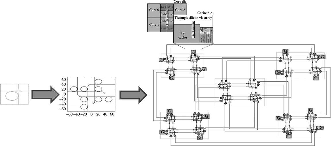
FIGURE 7.1 The pathfinding requirement.
A relevant gap separates baseline silicon photonic devices with on-chip communication architectures, which combine such devices together to materialize higher-order switching structures, complete communication channels, network topologies, routing and flow control methodologies, layout constraints aware physical designs. Network interfaces are an essential part of an ONoC architecture: their focus goes well beyond that of the low-level circuitry for domain conversion, but also covers typical networking topics such as proper buffer configuration and sizing, message-dependent deadlock avoidance, clock (re-) synchronization, end-to-end flow control, and so on.
The last group of researchers is instead involved in the redesign of an entire system to take the maximum advantage of the new interconnect technology. At this level, interconnect fabric design is tightly intertwined with system-level design issues such as memory organization, cache coherence protocol, application-perceived performance, number of memory controllers, and so on. Complex and scalable optical interconnects such as torus, square roots in J. Chan et al. [26], hierarchical wavelength-routed optical ring architectures in S. Koohi et al. [27], as well as Corona and Firefly frameworks [28,29] have been recently reported in this context.
Although many valuable research works have been reported in these emerging research fields, very few structured and coherent methodologies have been proposed so far (C. Batten et al. [30] is a nice example) to bridge the gap between the above abstraction layers for designing ONoC architectures. Such a pathfinding effort should address two relevant gaps that are highlighted in Figure 7.1. The first one exists between silicon photonic devices and on-chip communication architectures, which could be referred to as the physical gap. A design methodology addressing this gap should for instance deal with the deviation of physical topologies with respect to their logic schemes, take placement and routing constraints into close account for topology assessment and selection, engineer and optimize the electronic side of the network interface architecture, consider aggressive electrical baselines for the sake of crossbenchmarking, carefully include static power overhead in the overall power budget, or devise smart selection policies of network routes in hybrid electro-optical interconnect fabrics.
The second gap separates on-chip communication architectures with system-level design frameworks, and could be referred to as the systemability concern. Here, the focus is on the codesign of the ONoC architecture with the requirements dictated by the target system, and on future generations of such systems. Therefore, a design methodology addressing this gap should deal with scalability methods to hundreds of cores, cache coherence signaling, tuning ONoC parameters to system requirements, interconnect, and memory hierarchy codesign. The precondition to address the systemability gap in a trustworthy way is to enforce technology- and layout-aware decision making across all the layers of the design hierarchy, that is, to bridge the physical gap. Without that, conclusions of system-level studies about the potentials of optical interconnect technology turn out to be overly optimistic. The focus of this chapter is therefore on the characterization of the physical gap for the most relevant wavelength-routed ONoC (WRONoC) topologies, and on the evaluation of their robustness to the insertion loss degradation that takes place when refining the logic topology into the physical one. It will be showed that the predictability of a topology does not only depend on the careful back-annotation of physical parameters into its logic scheme, but also on taking the implications of place and route constraints on the actual topology layout into close account.
7.4 Predictability–Critical Optical Networks-on-Chip Topologies
Several connectivity patterns have been proposed for both space-routed and WRONoCs, however their properties are often discussed with reference to the logic scheme only. For space-routed ONoCs, which reserve the entire bandwidth of an optical path to a specific communication flow, this practice is likely to deliver accurate results just at the same as topologies are typically inspired by the regular ones in use in general purpose electronic NoCs (e.g., mesh, torus, spidergon) [26], see Figure 7.2a. This is a consequence of the good matching between the wavelength parallelism of space-routed ONoCs and the bit parallelism of electronic NoCs.
In contrast, WRONoCs are fundamentally different from electronic and space-routed optical networks, as they inherently deliver full connectivity (i.e., contention-free and potentially parallel communication between every master and every slave), while sharing the bandwidth of optical paths between multiple communication flows. WRONoC topologies are typically built up with optical add-drop filters [31]. On one hand, they split multiwavelength signals into their basic components, each one routed to a different destination. On the other hand, they aggregate signals from different masters (featuring different wavelengths) for each destination (see Figure 7.2b).
Although topologies differentiate themselves for the amount of physical resources (waveguides, optical filters) and number of wavelengths they require, they can be ultimately viewed as multistage interconnection networks (MINs), a connectivity pattern that maps inefficiently onto a 2D floorplan. In some cases, such networks are effectively folded to match specific placement constraints of masters and slaves, like for GWOR topologies (see Figure 7.2c). Unfortunately, the implications of different placement assumptions on topology properties are hard to predict. Clearly, designers that intend to leverage on the contention-free communication paradigm of WRONoCs have to deal with the design predictability gap of their topologies, assessing the deviation of topology layouts from their logical views, due to the placement constraints of network initiators and targets on the system at hand.
A typical experimental setting consists of deriving such constraints from the floorplan of a clusterized multicore processor with an optical layer vertically stacked on top of it, providing intercluster as well as processor-memory communication. In practice, they concern the actual position of optical network interfaces and photonically integrated memory controllers on the optical layer. The key sources of nonideality are the additional number of waveguide crossings, which derives from mapping the connectivity pattern on a 2D layout, and the propagation loss arising from long waveguides. Consequently, the ultimate implications of topology actual layouts on network total power consumption can be derived, as optical power losses need to be compensated by a higher power output by laser sources, in an attempt to feed photodetectors with enough optical power for reliable detection.
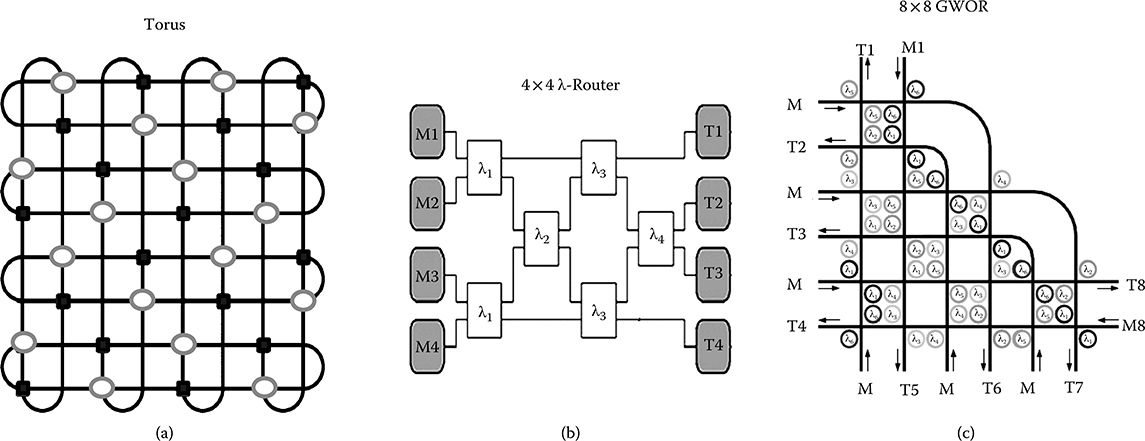
FIGURE 7.2 (a) Space-routed torus, (b) Wavelength-Routed λ-router, and (c) Generic Wavelength-Routed Optical Router (GWOR).
7.5 Design Space Exploration of Wavelength-Routed Topologies
To assess the role of placement constraints in the comparison framework of wavelength-routed network topologies, we need to make specific assumptions on the target system. As mentioned, 3D stacking is a promising scenario for the cost-effective integration of heterogeneous technologies. ONoCs are very likely to be integrated with electronic components in such an environment. Therefore, we focus on a 3D stacked multicore processor, consisting of an electronic layer and an optical one vertically stacked on top of it (see Figure 7.3). The electronic layer is composed by an array fabric of homogeneous processor cores (such as the Tilera architectures [5]), which are grouped into computation clusters. Without lack of generality, we assume that cores are aggregated into 4 clusters of 16 cores each, and that each cluster has its own gateway to the optical layer (vertically stacked with a corresponding hub in the optical layer). This latter accommodates three kinds of communications: (1) between any two pairs of clusters; (2) from a cluster to a memory controller of an off-chip photonically integrated DRAM DIMM [32]; and (3) from a memory controller back to a cluster. Finally, we assume a core size of 1 × 1 mm and a die size of 8 × 8 mm. In this context, placement constraints that are likely to be enforced during the place and route of network topologies are as follows.
First, hubs (i.e., the optical components of an electro-optical and optoelectronic network interface) should be positioned in the middle of each cluster, hence they end up being placed along a square in the middle of the optical layer (see Hi blocks in Figure 7.3).
Second, we assume 4 memory controllers located pairwise at the opposite extremes of the chip (see Mi blocks in Figure 7.3), as proposed in conventional chip multiprocessor architectures [33]. Overall, we need to connect eight initiators (four hubs, four memory controllers) with eight targets (the target interface of the same four hubs and four controllers). For this purpose, we leverage on a WRONoC topology. Global connectivity is clearly the easiest architectural solution that can be exploited to connect initiators and targets with each other. Therefore, this approach will initially be addressed. To provide global connectivity, an 8 × 8 WRONoC topology is required. Ultimately, the most relevant topology logic schemes that can address this connectivity requirement are discussed, followed by their implementation in the target system.
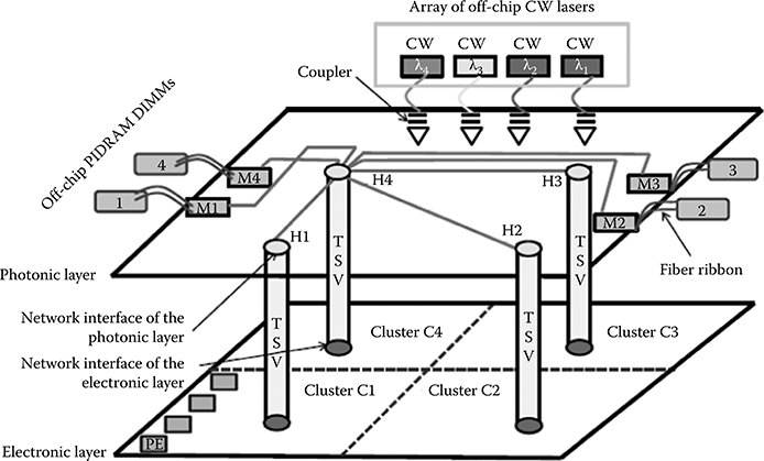
FIGURE 7.3 3D target architecture.
7.5.1 Global Connectivity
Figure 7.4a shows the first topology under test: an 8 × 8 λ-router, which was proposed by Scandurra and Connor [31]. To interconnect eight initiators with eight targets, the network utilizes eight stages of four and three add-drop filters. The topology reflects the connectivity pattern of unidirectional MINs in the electronic domain, where however the interstage pattern is custom-tailored for the routing methodology of WRONoCs. Unfortunately, the attractive logic scheme of this topology does not match the actual placement constraints of most real-life systems, where it is almost impossible to find all initiators on one side and all targets on the other side of the chip. At the same time, many cores are both initiators and targets of on-chip communication transactions, hence the physical implementation of this topology implies some degree of folding.
Due to the lack of consolidated automatic place and route tools for ONoCs, the connectivity pattern of all topologies were manually laid out, hence coming up with full custom design solutions. Figure 7.4d depicts the actual layout of the 8 × 8 λ-router topology after manual placement of MRRs, and routing of waveguides. Later validation experiments with prototype place and route tools delivered lower absolute numbers (waveguide crossings, insertion loss), but the same relative trends presented in this chapter [34]. In Figure 7.4, the central boxes in the layouts represent hubs, whereas the side ones represent memory controllers. For each box, the internal splitting lines denote initiator and target sections of network interfaces.
The followed layout design guidelines were inspired by and similar to those used to lay out fat-tree topologies in electronic NoCs [35]. Moreover, the criteria were a uniform exploitation of the floorplan space and the equalization of waveguide length. In spite of this, the difference between the logic and the physical topologies is still apparent. The ultimate effect is an increase of the total amount of insertion losses (dominated by waveguide crossings), which in turn leads to an increased requirement on the laser power needed by the optical signals to stay above the minimum detection threshold of the photodiodes.
To find the best solution for global connectivity, the previous topology is compared next with the 8 × 8 GWOR [17] and an optimized crossbar variant, hereafter referred to as the 8 × 8 folded crossbar.
According to the wavelength assignment proposed in X. Tan et al. [17], the 8 × 8 GWOR (see Figure 7.4b) is constructed starting from its lower basic cell, the 4 × 4 GWOR. This latter is well suited for those cases where initiators and targets are distributed across the cardinal points. In fact, the topology consists of four waveguides that intersect each other, with MRRs placed pairwise at each intersection. Unfortunately, the scaled pattern to an 8 × 8 network keeps making the same physical placement assumptions, which is not realistic, as it is very unlikely that all cores are placed around a central fence including the optical interconnect fabric.
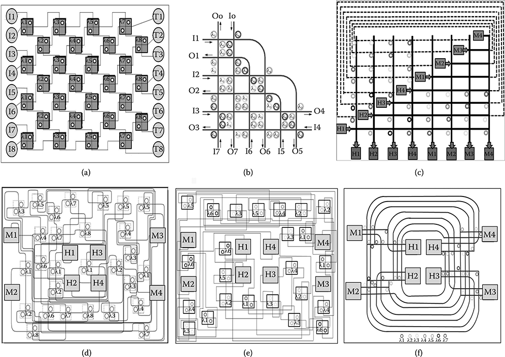
FIGURE 7.4 Logic topologies (a)–(c) versus corresponding physical topologies (d)–(f). Circles denote the micro ring resonators belonging to the interconnection network, whereas external boxes indicate initiators and targets (i.e., the inputs and outputs of the network).
Moreover, it is worth recalling that, unlike the previous topology, this one saves some resources by avoiding the useless self-communication capability. The physical view of the 8 × 8 GWOR is illustrated in Figure 7.4e, and confirms that the placement constraints of the target system are unnatural for the GWOR connectivity pattern, which ends up in a circuitous wiring that makes the original pattern hardly recognizable.
Again, the waveguide crossings arising as an effect of the 2D surface mapping are apparent. Finally, an 8 × 8 optical crossbar is considered. This topology places MRRs at each intersection of a point matrix, thus establishing connections between a given initiator and the desired target. Although considered quite inefficient in abstract analysis frameworks, the topology lends itself to an interesting optimization that applies directly to its logic scheme. In the original topology, every initiator delivers optical signals to targets in a given order. By changing this order for every initiator (see Figure 7.4c), then a waveguide length overhead is apparently generated (see the wraparound links). However, this is only an apparent effect of the logic scheme, as the actual layout is in contrast facilitated: every initiator can in fact drive an optical waveguide that is part of a ring-like topology that dispatches optical packets to the possible destinations (Figure 7.4f). Moreover, the logic scheme of this topology makes only use of 1 × 2 optical filters with respect to other topologies, which instead basically use 2 × 2 optical filters. Clearly, the layout is much more regular than the 8 × 8 λ-router and the 8 × 8 GWOR, and MRRs are clearly positioned close to communication targets for wavelength-selective ejection of optical signals. In previous comparison frameworks, such layout-level details are typically omitted, and considered quality metrics include mainly the number of MRRs, and the maximum number of waveguide crossings on the logic scheme. From this viewpoint, the 8 × 8 folded crossbar features the lowest number of MRRs (44), as opposed to 48 for the 8 × 8 GWOR, and 56 for the 8 × 8 λ-router. Unfortunately, this analysis methodology is only partially informative and even misleading. The ranking is in fact exactly the opposite when the number of waveguide logic crossings is considered: the λ-router would exhibit 7 crossings as opposed to the 10 ones of GWOR and the 15 ones of the optical crossbar. Clearly, such abstract and even conflicting considerations alone are not enough to derive trustworthy conclusions, especially when the most power-efficient solution is searched for. For this reason, physical layer and layout analysis are required to assess the real trade-offs. Finally, it is important to keep in mind that optical crossbar and GWOR utilize seven distinct wavelengths (i.e., seven continuous-wave laser sources) by construction to deliver full and global connectivity versus the eight ones of an 8 × 8 λ-router.
7.5.2 Relative Topology Comparison
Insertion loss is the most important physical metric that must be quantified to determine the laser power that guarantees a predefined bit error rate at receivers. In fact, once ILmax is obtained (the maximum insertion loss across all wavelengths and optical paths), and the detector sensitivity is known (S), it is possible to evaluate the lower limit of optical laser power (P) to reliably detect the corresponding photonic signal at the receiver end. A simplifying assumption can be made at this point: the worst-case ILmax can be quantified across the entire global network, and then the practical assumption can be made that such a worst-case ILmax dictates the power output by all laser sources. This study assumes the loss parameters summarized in Table 7.1. A Simulink® simulation framework is used to assess physical metrics of ONoCs by modeling every single path of a given topology while accounting for the above loss parameters. Finally, the corresponding insertion loss is obtained as a sum of all components losses such as PSEs, straight, bend, crossing waveguides, and drop-into ring losses encountered in the path under test. The topology models assume die sizes of 8 × 8 mm. Figure 7.5 shows insertion loss deviations between logic and physical ONoCs for all topologies considered in this comparison framework, when the standard elliptical tapers are assumed at every waveguide crossing [6]. The insertion loss critical path is more than six times worse in two physical networks out of three with respect to the corresponding logic schemes. Especially GWOR suffers from 72 waveguide crossings against the 10 expected ones, whereas λ-router reports 64 crossings versus 7. Surprisingly, the folded crossbar maps more efficiently to the target placement constraints, although it is frequently discarded in abstract analysis frameworks, which only consider the logic schemes and the abstract properties. The physical implementation is so efficient (i.e., only very few additional crossings from layout constraints) to offset the inherently higher number of waveguide crossings of the logic scheme. More in details, propagation loss is a significant contribution in the folded crossbar topology, indicating that the critical path now is both waveguide- and crossing-dominated. Due to its long optical waveguide of 25.5 mm (worst case) and 22 crossings, the folded crossbar achieves 15.3 dB optical power loss on the critical path. On the contrary, for λ-router (33.3 dB) and GWOR (37.5 dB) only crossing losses have been computed as their contribution is dominant in the breakdown. Obviously, had we accounted for their propagation losses too, their current huge gap with the crossbar would have become even worse, without providing any significant novelty to the discussed results.
Table 7.1 Loss Parameters
Parameters |
Value |
Propagation loss from J. Chan et al. [26] |
1.5 dB/cm |
Bending loss from J. Chan et al. [26] |
0.005 dB |
Crossing loss (optimized by elliptical taper) from 2D FDTD |
0.52 dB |
Drop loss (optimized by elliptical taper) from 2D FDTD |
0.013 dB |
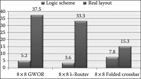
FIGURE 7.5 Maximum insertion loss across topologies.
By using the critical path insertion loss, it is then possible to derive the needed laser power to get a bit error rate of BER=10−12 at optical receivers with a sensitivity of -17 dBm [36]. By also considering the contribution of modulator [37] and detector power [36], and of thermal tuning [26] listed in Table 7.2, the total power results in Figure 7.6 can be derived. The total power of GWOR is larger than that of other topologies, even if the λ-router features one laser source more than GWOR and the folded crossbar to provide the same (full) connectivity. More precisely, the total power of the λ-router topology is 2.47 times lower than the GWOR one. The folded crossbar turns out to be the most power efficient solution. It consumes only 276 mW, almost two orders of magnitude less than GWOR. These results certainly indicate that GWOR and λ-router are unfeasible for the placement constraints of the target 3D system, at least when they target global connectivity.
Table 7.2 Device Parameters
Device |
Features |
Laser |
CW (continuous-wave) Laser efficiency PLE = 20% Coupling laser-link PCW = 90% |
Modulator |
Silicon-disk Launch-efficiency β = 20% Dyn. dissipation = 3 fj/bit Static power = 30 μW Vdd = 1 V Modulator-power depends on ILmax [37] |
Detector |
CMOS (45 nm) Hybrid silicon receiver Sensitivity, S = −17 dBm (BER = 10−12 at 10 Gbit/s) Power = 3.95 mW [36] |
Photonic-switching-elements |
Thermal tuning = 20 μW/ring [26] |
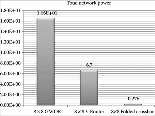
FIGURE 7.6 Total network power across topologies.
7.5.3 Comparison with an Optical Ring Topology
The layout of the folded crossbar is very similar to a ring topology. This latter is in fact the simplest connectivity solution among all network topologies presented in the open literature, and apparently the less sensitive one to place and route constraints. The only one way to assess whether the folded crossbar is the most efficient solution for the target system consists of comparing it with an actual ring topology. To correctly compare these topologies, a ring is designed assuming the same number of wavelengths utilized in the crossbar, that is, seven. The use of multiple ring waveguides (i.e., spatial division multiplexing) is the only way to meet this requirement. Figure 7.7b depicts the real layout of the ring topology after manual placement of the 3D stacked optical layer under test with the given physical constraints (i.e., hubs in the middle and memory controllers positioned at the opposite extremes). Clearly, this topology better fits the target constraints. Essentially, it works like a bus, in which multiple waveguides are contained into it. In this case, seven parallel waveguides are needed to deliver full and contention-free communication parallelism. Figure 7.8a illustrates the postlayout insertion loss critical path comparison between the 7-way ring and the 8 × 8 folded crossbar.
The 7-way ring achieves 7.75 dB insertion loss against 15.3 dB of the crossbar on the critical path, thus resulting 50% more power efficient. The key reason lies in the fact that the 7-way ring provides less wiring length on the critical path (2 vs. 2.55 cm in the crossbar). Moreover, the crossbar has 22 waveguide crossings (localized in the optical network), while only 9 crossings are there in the 7-way ring. Even if in the ring topology, there are no intersections in principle, they are actually needed at initiator interfaces to connect to the parallel ring waveguides that are furthest away from the injection point, as shown in Figure 7.7a. In contrast, such crossings may not appear at target interfaces, since the output signal of photodetectors might directly leave the optical plane by means of through-silicon vias (TSVs) in the best case. Notice that the logic scheme of any ring topology is characterized by such obstacles, which may degrade the insertion loss, and as a consequence the total power. In this case, ILmax of the ring logic scheme is about 4.7 dB, while it gets almost doubled when postlayout results are considered. Here, the wiring length contribution becomes dominant through its propagation loss.
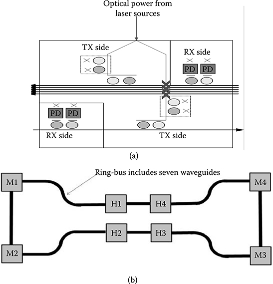
FIGURE 7.7 (a) Optical network interface architecture. (b) Manual layout of an optical ring topology.
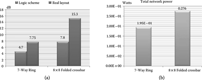
FIGURE 7.8 (a) ILmax. (b) Total network power for the topologies under test.
The total power consumption of the two topologies is shown in Figure 7.8b. Thanks to the lower insertion loss, the 7-way ring topology results more efficient than the 8 × 8 folded crossbar by about 30%. This latter is heavily penalized by the larger number of crossings, and the higher wiring length. In this case, the insertion loss gap of 50% is reduced to 30% in terms of total power, due to the relevant contribution of optical receivers in the breakdown. They contribute for 63% in the crossbar topology and for 89% in the ring one.
Ultimately, the optical ring is clearly an appealing solution for such a small scale system. However, in highly integrated systems the picture is not entirely clear, as the larger connectivity requirements cause the number of ring waveguides to increase, hence worsening the crossing concerns at initiator interfaces. At the same time, in larger dies the critical path becomes propagation loss dominated, thus raising another concern for optical rings. Finally, the quality metrics of filter-based topologies will be effectively scaled up in future systems as computer-aided design (CAD) tools for automatic place and route of ONoC topologies become available.
7.5.4 Network Partitioning
To increase the level of confidence of this comparative framework, optimization techniques well beyond global connectivity are worth exploring such as network partitioning for wavelength reuse (all topologies) and topology transformations for the optical crossbar and GWOR topologies for more flexible and/or efficient place and route. This work does not blindly apply topologies under test to the master/slave connectivity problem of the target system, as the previous section has demonstrated that even at such a small system scale, a typical global topology for all communication actors becomes easily infeasible: too many waveguide crossings arise in an attempt to accommodate the connectivity pattern onto the 2D floorplan. Of course, should the routing methodology change (e.g., arbitration of waveguides), the picture would change again and deserve further analysis.
Network partitioning is considered in this analysis framework, not only as a means of increasing design predictability but also of enabling wavelength (and laser source) reuse across partitions, similar to what is done in telecommunication networks.
In particular, each network partition can be devoted to a specific traffic class, namely intercluster communications, memory access requests from clusters, and memory responses from memory controllers.
A separate network, and associated topology, can be inferred in each partition. Finally, this strategy enables to cut down on the number of wavelengths from eight to just four, thanks to their reuse.
7.5.5 Logic Topologies
This section illustrates the logic schemes of WRONoC topologies under test, considering that each network partition will have to interconnect at most four masters with four slaves. We consider the most relevant schemes that have been proposed so far in the open literature (the same used for global connectivity, although scaled down), in addition to engineering an ad-hoc topology for the 3D stacked system at hand.
As mentioned in the previous paragraph, the 8 × 8 GWOR is a scalable and non-blocking wavelength-routed optical router. The basic cell of the former solution is represented by the 4 × 4 GWOR that has four bidirectional ports located on the cardinal points. Furthermore, two horizontal and two vertical waveguides are used, which intersect each other to form a basic check shape, and MRRs are placed pairwise on waveguide intersections. The proposed topology does not support self-communication, hence its use for the memory request and response networks requires its extension to a 5 × 5 configuration. This is possible, as its wavelength assignment enables any size of GWOR architecture. As it can be seen in Figure 7.9a, 5 × 5 GWOR is constructed starting from its lower basic cell (4 × 4 GWOR). With respect to the baseline scheme, three more MRRs need to be inserted to work around the lack of self-communication, and enable each master to be connected with all of the four slaves. At the same time, one input goes unused, therefore redundant MRRs are removed.
On the contrary, Figure 7.9c illustrates the 4 × 4 λ-router. To interconnect four masters with four slaves, the network makes use of four stages of two and one add-drop optical filters. This network is obtained by scaling down the previously proposed 8 × 8 λ-router, or vice versa it could be seen as the preliminary cell to build any size of the λ-router network. With respect to the original scheme, the native 2 × 2 add-drop filters are replaced with 2 × 2 photonic switching elements, the only difference being an easier physical design thanks to the orthogonally intersected waveguides. Figure 7.9b shows the scaled-down version of the 8 × 8 folded crossbar, that is customized for connecting four initiators with four targets.
Finally, a custom-tailored solution for processor-memory communication is described, namely the Snake topology. The pattern (Figure 7.9d) is also flexible, as a different number of initiators and targets can be easily accommodated. In the 4 × 4 Snake, six wavelength filters (2 × 2 PSEs) are tuned to different wavelengths, and their number scales up from the upper side to the lower one. Four main optical links connect the slaves, while enabling some placement flexibility.
With respect to the λ-router, such a topology first breaks the monodimensional assumption, and also grows vertically instead of horizontally. In the end, the Snake is easily capable of providing asymmetric solutions (e.g., 4 × 8, 8 × 4), much more easily than λ-router (although this is in principle still feasible with this topology as well).
Finally, the Snake topology is conceived to map efficiently to the placement constraints of the target system, and should be viewed as a custom-tailored solution for the system at hand to ease reachability of memory controllers. In practice, communication from the center of the chip to its upper or lower side is facilitated.
For the sake of comparison, all topologies are constrained to use the same number of wavelengths and laser sources, and to instantiate physical resources accordingly. Therefore, all topologies have to deliver the same communication bandwidth.
Ultimately, as it was done for global connectivity, an optical ring topology is designed to connect four masters with four slaves, and then added in the comparison framework. In practice, rings are devoted to specific message classes in this instance (hereafter referred to as ORNoC).
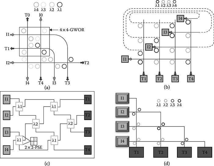
FIGURE 7.9 Network partitioning logic schemes (a)–(d). Circles denote the micro ring resonators belonging to the interconnection network, whereas external boxes indicate initiators and targets (i.e., the inputs and outputs of the network).
7.5.6 Physical Topologies
This section deals with the problem of assigning topologies to network partitions and of laying them out. For the intercluster ONoC, the choice is straightforward: 4 × 4 GWOR delivers the needed connectivity in a scenario where its physical placement assumptions are perfectly satisfied. At the same time, it features the lowest number of MRRs. Therefore, the problem can be restricted to identifying the topologies that are better suited for processor-memory communication, and to lay them out twice: for the memory request network (from hubs to memory controllers), and the memory response one (from controllers to hubs). The fundamental difference lies in the flipped position of masters and slaves, which makes them asymmetric.
Manual layouts have been drawn with similar criteria to those used for global connectivity. The only approximation lies in the lack of a distribution network of optical power. It is as though we were neglecting the top-level clock tree in the layout of an electronic network. After topology place and route, the difference between logic and physical topologies is still apparent although the use of network partitioning mitigates this effect to a significant extent.
The 5 × 5 GWOR (Figure 7.10a) suffers from the different placement position of network interfaces with respect to the logic scheme, to such an extent that the critical path increases from 4 crossings to 31, whereas the total number of MRRs achieves 40 (8 in the intercluster network, plus both 16 for the memory request network and the response one).
Despite a higher worst-case number of crossings in the logic scheme (6), the layout of the 4 × 4 folded crossbar in Figure 7.10b results only in 21 crossings, with the same number of MRRs reported by GWOR (40).
The layouts of the 4 × 4 λ router (Figure 7.10c), ORNoC (Figure 7.10d), and 4 × 4 Snake (Figure 7.10e) are clearly less intricate than the previous ones, hence potentially resulting in lower insertion loss critical paths. More precisely, λ-router reports eight crossings, whereas Snake only six.
By using the wavelength assignment in S. Le Beux et al. [38], and a convenient ordering of nodes along waveguides, ORNoC turns out to exhibit three crossings on the critical path, all localized close to network interfaces for the sake of waveguide reachability.
The key properties of the topologies under test, measured after their physical design and inclusive of the three partitions, are the following:
Although all topologies natively use four wavelengths, a spatial division multiplexing over four waveguides has to be used for ORNoC to achieve the same goal.
Snake and λ-router solutions make use of 32 MRRs (24 in the request and response networks vs. 8 in the intercluster one) against 40 of the ring one.
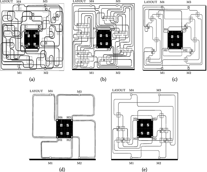
FIGURE 7.10 Topology layouts: (a) Generic Wavelength-Routed Optical Router (GWOR), (b) Folded Crossbar, (c) λ-router, (d) Ring, and (e) Snake.
The key reason lies in the fact that each optical network interface in the ring needs four MRRs to inject modulated wavelengths into their waveguides, in addition to eight MRRs needed in the intercluster network.
All other topologies instead do not have any injection filters, as they get a branch of the light distribution network, which directly enters the network. In the ring, the injection waveguide needs to be bridged to the ring waveguides. Extraction filters at receivers are common for all topologies, hence are not considered in the count.
7.5.7 Power Efficiency of Topologies
Figure 7.11a shows the worst-case insertion loss across all topologies considered in this comparison, assuming two kinds of tapers for the optimization of waveguide crossings: the standard elliptical taper and the MMI one.
However, the feasibility of the MMI taper should not be taken for granted, as it depends on the maturity of the manufacturing process, and on the device size. In fact, it has a larger area footprint with respect to the elliptical taper, therefore, it might be suitable for layout-induced waveguide crossings, but might be unfeasible for the internal crossings of photonic switching elements, where ring resonators should be placed close to the waveguides for the sake of efficient coupling. The insertion loss parameters utilized for this optimization were derived from 2D finite-difference-time-domain (FDTD) simulations. In particular, the crossing loss is about 0.18 dB while the drop loss exhibits 0.0087 dB.
GWOR turns out to be the worst solution, as it suffers from 31 crossings and 24 mm of wiring length on the critical path, whereas ORNoC (the best solution) has just 3 crossings but 32 mm of waveguides length as always on the critical path.
The Snake topology, with its six crossings and the same maximum guide length of GWOR, becomes competitive, as propagation losses are not very relevant at this chip size yet.
With elliptical taper, the overhead with respect to ORNoC is just 5%. 4 × 4 λ router has reasonable results in the comparison as it has 22 mm of wiring length and eight crossings, whereas the 4 × 4 folded crossbar is better than GWOR for two reasons: lower number of crossings (21), and a 4 mm shorter link length on the insertion loss critical path.
The effect of MMI is highly beneficial for the Snake, as it minimizes the impact of its crossings over ILmax, whereas benefits are not so relevant for the waveguide-dominated ORNoC.
This latter ends up in a 13.2% higher insertion loss than Snake. This result is very interesting, as it points out that there is actually a role also for nonring topologies in WRONoCs, in spite of their apparently higher complexity. In turn, Snake results in a 2.5%, 32.6%, and 49.5% lower insertion loss than λ-router, folded crossbar and GWOR respectively.
By using such critical path insertion losses, it was possible to derive the needed laser power to meet a BER of 10−12 at the optical receivers with a fixed sensitivity of -17 dBm. It is then possible to account for the power contribution of modulators, detectors, and thermal tuning, thus estimating total power for each topology. Relevant parameters are in Table 7.2.
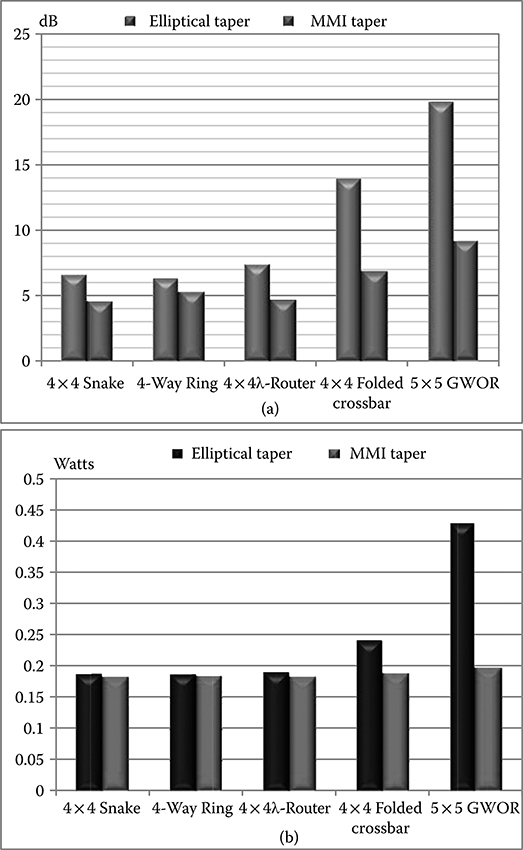
FIGURE 7.11 (a) ILmax. (b) Total network power comparison among topologies.
Figure 7.11b shows the total power across all topologies when the energy consumption of the detector is 395 fj/bit (or 3.95 mW). Power refers to the scenario where the maximum aggregate bandwidth of the network is used (around 440 Gbit/s with modulation rates of 10 Gbit/s).
As it can be seen, the total power of GWOR is higher than that of other topologies regardless of the specific taper. With elliptical tapers, GWOR is clearly infeasible under the given place and route constraints. The same holds, for the folded crossbar. The capability of the Snake topology to track power efficiency of the optical ring (the best solution) is remarkable at this system scale.
The effect of MMI tapers is to reduce the critical path differentiation across topologies, hence significantly bridging the gap between the best and the worst one.
Laser and modulator power are closely related to the ILmax of the topologies, however the total network power is dominated by receiver power with current technology assumptions (average 75% with elliptical taper as opposed to 90% with MMI taper), therefore, the remaining gap between topologies in Figure 7.11a maps to the total power gap of Figure 7.11b after going through an attenuation factor: just 15 mW of difference between Snake (the best) and GWOR (the worst). Of course, different laser sources (e.g., wall-plug laser efficiency) or receiver (e.g., energy) parameters may further widen the gap.
7.5.8 Global Connectivity Versus Network Partitioning
This section describes the comparison between the best topologies, both ring-based and filter-based, implemented both for global connectivity and network partitioning.
Figure 7.12a shows the total power comparison between the message-class-specific rings (from partitioning optimization) and the global ring. As it can be seen, both implementations almost provide the same total power, particularly, the partitioned ring consumes 188 mW, instead the global one 195 mW (roughly 3.6% more). This marginal deviation is determined by the laser power. In particular, the global ring topology features more laser sources then the local ring (seven vs. four). Let us denote also that the receiver power results to be the most important contributor in the power breakdown.
In contrast, Figure 7.12b illustrates the total power comparison of the best filter-based topologies, both in the global connectivity and the network partitioning cases. Similar to ring-based topologies, the receiver power significantly contributes to the total power. However, for the 8 × 8 folded crossbar (the best global topology) such impact ends up being mitigated by modulator power, that becomes relevant as the 8 × 8 folded crossbar topology provides higher insertion loss than the 4 × 4 Snake (15.3 dB vs. 6.75 dB). It should be recalled that modulator power partly depends on the input optical power. By including all contributions, the 4 × 4 Snake results to be more efficient than the 8 × 8 folded crossbar by about 30% (189 vs. 276 mW).
From the proposed analysis, it is clear that filter-based topologies benefit the most from the network partitioning optimization, whereas ring topologies are in any case global structures. Also, in small-scale systems topology selection can be ultimately dictated by design simplicity considerations, as it is not difficult to engineer both filter-based and ring-based topologies with similar power figures. From this viewpoint, ring solutions are clearly appealing.
7.6 Optical Ring Versus Filter-Based Topology in Scaled Systems
As the next step, the impact of system scale and technology evolution over the illustrated trend is characterized. For this purpose, a future generation of the target system is projected.
Let us now assume 128 cores in the tile-based electronic plane, getting access to the optical layer through eight gateways (and eight corresponding hubs in the optical plane). The number of memory controllers can be kept the same, which might be feasible due to the benefits of photonics integration deeper into the DRAM DIMM [11]. Consequently, the die size grows to 16 × 16 mm.
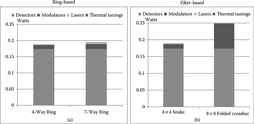
FIGURE 7.12 (a) Partitioned versus global Ring topology. (b) Best partitioned (4 × 4 Snake) versus best global (8 × 8 folded crossbar) topologies.
We limit the comparison between ORNoC and the best filter-based topology found so far, that is, the partitioned Snake, and omit the intercluster network. Therefore, two four-waveguide ORNoCs and two separate Snake topologies (an asymmetric 8 × 4 network for memory requests, and a 4 × 8 one for responses) are considered.
MMI tapers are assumed to be mainstream in the implementation of these topologies, and detector energy is assumed to be improved up to 50 fj/bit [26], while conservatively preserving the same receiver sensitivity, a projection that is supported by the physical considerations in M. Georgas et al. [39] about silicon photonics in 3D stacked systems and receiver circuitry.
Figure 7.13a shows the insertion loss critical path breakdown of each topology.
The ring architecture (built on eight waveguides) is in fact heavily penalized by the high-wiring length over the new die size (64 vs. 48 mm of Snake), which leads to a larger amount of propagation loss regardless of the higher number of crossing losses in Snake (1.75× higher than the ring).
The total power consumption across the two topologies is shown in Figure 7.13b. Thanks to the lower insertion loss on the critical path and the higher maturity of receiver technology, the Snake results more efficient than the ring architecture by about 15%. This certainly confirms that optical ring topologies are not the most power efficient and least complex solution in all WRONoC scenarios, but that conclusions are tightly instance- and technology-specific. As the technology is still admittedly in the early stage, it is currently not possible to drop neither rings nor filter-based topologies for future ONoC topology design.
7.7 Conclusion
This chapter argued a comparative analysis of WRONoC topologies by considering both the properties of optical links as well as placement constraints on a target system of practical interest.
First, there is a large deviation of insertion loss between the logic scheme and the physical implementation as an effect of placement constraints.
Second, the most promising logic schemes may turn out to be the worst physical topologies, so the design predictability gap should be carefully quantified.
Third, network partitioning is an effective way of reusing wavelengths and simplifying ONoC design.
Fourth, the best topologies for global connectivity are not necessarily the best options for network partitioning.
On one hand, for small scale systems, a spatial division multiplexed ring topology is hard to beat. Even in this context, should technology evolutions improve optical receiver energy, filter-based networks could again have a role. In practice, an optical ring is ideally the best WRONoC topology, but its practical nonidealities (e.g., waveguide reachability in the injection system, worse waveguide length scalability on the critical path) make an actual comparative test with other filter-based topologies mandatory in the target system.
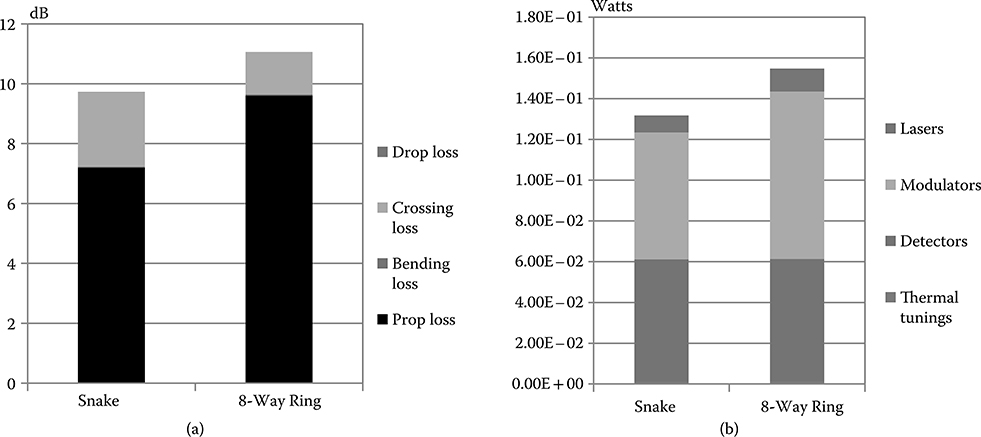
FIGURE 7.13 (a) ILmax. (b) Total network power Snake versus Ring architecture.
On the other hand, for future larger scale systems, where connectivity requirements and die size increase, spatial division multiplexing combined with the relevant role of propagation losses seriously penalizes optical ring architectures, so that filter-based topologies may become appealing. This trend will be further consolidated by the development of CAD tools for automatic place and route of filter-based topologies, which will optimize their quality metrics in layout-intricate and/or highly integrated scenarios.
References
1. D. A. B. Miller, Rationale and challenges for optical interconnects to electronic chips, Proc. IEEE, 88(6), 728–749, 2000.
2. D. Marris-Morini et al., HELIOS project: Deliverable D010: State-of-the-Art on Photonics on CMOS, October 2011.
3. ePIXfab: The silicon photonics platform.
4. A. Biberman and K. Bergman, Optical interconnection networks for high-performance computing systems, Rep. Prog. Phys., 75(4), 2012.
5. B. G. Lee et al., Ultrahigh bandwidth silicon photonic nanowire waveguides for on chip networks, IEEE Photonics Technol. Lett., 20, 398–400, 2008.
6. N. Sherwood-Droz et al., Optical 4x4 hitless silicon router for optical networks-on-chip (NoC), Opt. Express, 16(20), 15915–15922, 2008.
7. G. R. Hadley, Effectivesurface-emitting lasers, Opt. Lett., 20, 1483–1485, 1995.
8. A. Biberman et al., Photonic network-on-chip architectures index model for vertical-cavity using multilayer deposited silicon materials for high-performance chip multiprocessors, ACM J. Emerg. Technol. Comput. Syst., 7(2), 7:1–7:25, 2011.
9. N. Ophir et al., Demonstration of 1.28 Tb/s Transmission in Next Generation Nanowires for Photonics Networks-n-Chip, 23rd Annual Meeting of the IEEE Photonic Society, pp. 560–561, Denver, CO, November 7–11, 2010.
10. S. Manipatruni, Q. Xu, B. Schmidt, J. Shakya, M. Lipson, High Speed Carrier Injection 18 Gbit/s Silicon Microring Electro-Optic Modulator, 20th Annual Meeting of the IEEE Lasers and Electro-Optics Society, Lake Buena Vista, FL: IEEE, 537–538, 2007.
11. K. Preston, P. Dong, B. Schmidt, M. Lipson, High-speed all optical modulation using polycrystalline silicon microring resonators, Appl. Phys. Lett., 92, 151104, 2008.
12. B. G. Lee, A. Biberman, P. Dong, M. Lipson, K. Bergman, All-optical comb switch for multiwavelength message routing in silicon photonic networks, IEEE Photonics Technol. Lett., 20(10), 767–769, 2008.
13. H. Gu, K. H. Mo, J. Xu, W. Zhang, A Low-Power Low-Cost Optical Router for Optical Networks-on-Chip in Multiprocessor Systems-on-Chip, IEEE Computer Society Annual Symposium on VLSI, Tampa, FL: IEEE, 19–24, 2009.
14. H. Gu et al., A Low-Power Fat Tree-Based Optical Network-on-Chip for Multiprocessor System-on-Chip, DATE: Conference on Design, Automation and Test in Europe, Nice, France: IEEE, 3–8, 2009.
15. I. O’Connor et al., Toward Reconfigurable Optical Network on Chip. ReCoSoC: Reconfigurable and Communication-Centric Systems-on-Chip, Univ. Montpellier II, France, 121–128, 2005.
16. L. Ramini, P. Grani, S. Bartolini, D. Bertozzi, Contrasting Wavelength-Routed Optical NoC Topologies for Power-Efficient 3D-Stacked Multicore Processors Using Physical-Layer Analysis, DATE: Conference on Design, Automation and Test in Europe, Grenoble, France: IEEE, 1589–1594, 2013.
17. X. Tan et al., On a Scalable, Non-Blocking Optical Router for Photonic Networks-on-Chip Designs, Photonics and Optoelectronics (SOPO), Wuhan, China: IEEE, 2011.
18. S. Assefa et al., CMOS-integrated high-speed MSM germanium waveguide photdetector, Opt. Express, 18(5), 4986–4999, 2010.
19. T. Yin et al., Ge n-i-p waveguide photodetectors on silicon-on-insulator substrate, Opt. Express, 15(21), 13965–13971, 2007.
20. M. W. Geis et al., Silicon waveguide infrared photodiodes with > 35 GHz bandwidth and phototransistors with 50 A/W-1 response, Opt. Express, 17, 5193–5204, 2009.
21. O. Jambois, Towards population inversion of electrically pumped er ions sensitized by Si nanostructures, Opt. Express, 18, 2230–2235, 2010.
22. I. Yoiung, E. Mohammed, J. Liao, A. Kern, S. Palermo, B. Block, M. Reshotko, P. Chang, Optical I/O Technology for Tera-Scale Computing, ISSCC, Dig. Tech. Papers, 45(1), 468–469, 2009.
23. F. Liu et al., 10 Gbps 530fJ/b Optical Transceiver Circuit in 40 nm CMOS, Symposium on VLSI Circuit, 290–291, June 2011.
24. A. Huang et al., A 10Gb/s photonic modulator and WDM MUX/DEMUX integrated with electronics in 0.13 µm SOI CMOS, Solid-State Circuits Conference ISSCC 2006, Dig. Tech. Papers, San Francisco, CA: IEEE, 922–929, 2006.
25. J. Orcutt et al., Open foundry platform for high-performance electronic-photonic integration, Opt. Express, 20(11), 12222–12232, 2012.
26. J. Chan et al., Architectural exploration of chip-scale photonic interconnection network designs using physical-layer analysis, J. Lightwave Technol., 28(9), 1305–1315, 2009.
27. S. Koohi, M. Abdollahi, and S. Hessabi, All-Optical Wavelength-Routed NoC Based on a Novel Hierarchical Topology, NOCS’11: International Symposium on Networks-on-Chip, Pittsburgh, PA: IEEE, 97–104, 2011.
28. D. Vantrease et al., Corona: System Implications of Emerging Nanophotonic Technology, International Symposium on Computer Architecture, 153–164, Beijing, China, 2008.
29. Y. Pan, P. Kumar, J. Kim, G. Memik, Y. Zhang, and A. Choudhary Firefly: Illuminating Future Network-on-Chip with Nanophotonics, International Symposium on Computer Architecture, p. 429440, Austin, TX, June 2009.
30. C. Batten et al., Designing chip level nanophotonic interconnection networks, Emerging and selected topics in circuits and systems, IEEE Journal, 2(2), 137–153, 2012.
31. A. Scandurra and I. O’Connor, Scalable CMOS-Compatible Photonic Routing Topologies for Versatile Networks on Chip, Network on Chip Architecture, 2008.
32. Scott Beamer et al., Re-Architecting DRAM Memory Systems with Monolithically Integrated Silicon Photonics, 37th ACM/IEEE International Symposium on Computer Architecture (ISCA), 2010.
33. D. Wentzlaff et al., On-Chip Interconnection Architecture of the Tile Processor, IEEE Micro, 27(5), 15–31, 2007.
34. A. Boos, L. Ramini, U. Schlichtmann, D. Bertozzi, PROTON: An Automatic Place-and-Route Tool for Optical Networks-on-Chip, ICCAD’13: International Conference on Computer Aided Design, San Jose, CA: IEEE, 2013.
35. D. Ludovici et al., Assessing Fat-Tree Topologies for Regular Network-on-Chip Design under Nanoscale Technology Constraints, DATE’09: Conference on Design, Automation and Test in Europe, Nice, France: IEEE, April 2009.
36. Xuezhe Zheng et al., Ultra-efficient 10Gb/s hybrid integrated silicon photonic transmitter and receiver, Optical Society of America, 2011.
37. D. A. B. Miller, Energy Consumption in optical modulators for interconnects, Optical Society of America, 2012.
38. S. Le Beux et al., Optical Ring Network-on-Chip (ORNoC): Architecture and Design Methodology”, DATE: Conference on Design, Automation and Test in Europe, Grenoble, France: IEEE, 788–793, 2011.
39. M. Georgas et al., A monolithically-integrated optical receiver in standard 45-nm SOI, Solid-State Circuits, 47, 1693–1702, 2002.