
9 Nanoelectromechanical Relays
An Energy Efficient Alternative in Logic Design
Ramakrishnan Venkatasubramanian and Poras T. Balsara
Contents
9.2 CMOS Replacement Devices: Mechanical Relays
9.2.1 Electrostatically Actuated Nanoelectromechanical Relay Devices
9.2.2.1 Cantilever Beam and Laterally Actuated NEM Relays
9.3 Verilog-A Model of Suspended Gate Relay
9.3.1 Definition of NEM Relay Parameters
9.3.2 Electromechanical System Model
9.4 NEM Relay–Based Digital Logic Design
9.4.1 Intrinsic Capacitance of the Relay (Cint)
9.4.1.1 Relay-Based Latch Circuits
9.4.1.2 Relay-Based Flop Circuits: Tristate Relay Flop
9.4.1.3 Max Frequency of Operation and Min-Pulse Width
9.4.1.4 Performance, Energy, and Area Comparison
9.4.1.5 Improving Performance of NEM Relay Circuits Using Charge Boosting
9.5 NEM Relay–Based Memory Design
9.5.1 Three-Relay Random Access Memory (3RRAM)
9.5.2 Two-Relay Random Access Memory (2RRAM)
9.5.3 P4RRAM: Parallel 4R RAM Bitcell
9.5.4 P3RRAM: Parallel 3R RAM Bitcell
9.1 Introduction
Complementary metal–oxide–semiconductor (CMOS) transistor scaling over the last 30 years has enabled significant integration of complex electronic circuitry providing improvements in switching speed, density, cost, and functionality of CMOS chips [1]. However, as the thermal voltage kT/q does not scale, the threshold voltage (VT) of CMOS transistors cannot be reduced along with the lithographic dimensions [2]. The threshold voltage of CMOS transistors in the sub-40-nm regime has already been scaled to a value that balances leakage energy and dynamic energy optimally [3]. Further reduction in the threshold voltage would actually increase the amount of energy consumed per operation. Further, there is not much supply voltage scaling expected in smaller technology nodes because of the thermal limit (kT/q) [4,5].
Because of these inherent limitations in continual CMOS scaling and increasing power density of integrated circuits due to larger, faster electronic circuits [6], researchers have focused on improving energy efficiency of CMOS circuits. This has led to multicore processing, that is, recover system throughput through parallelism. The benefits of this approach are limited as well, because a minimum in total energy is reached when the active energy and leakage energy are balanced and further VDD reduction will only increase the total energy per operation. The subthreshold slope of CMOS shown in Figure 9.1 is approximately 60–70 mV/decade. To achieve greater energy efficiency in logic circuits, there is always a quest to develop new devices with steeper subthreshold slopes with the ultimate goal of developing an ideal switch with zero off-state current as shown in Figure 9.1. Alternative transistor designs like the tunnel field effect transistor (FET) [7] with steeper subthreshold slope have been proposed. However, they are also fundamentally limited in energy efficiency because of nonzero off-state current.
Furthermore, CMOS logic circuit operation is susceptible to extreme environmental conditions; for example, CMOS cannot function effectively over 150°C. This poses a major limitation for usage of CMOS circuits in harsh and extreme environments such as space, defense, and operating environments with high radiation levels. Typically, electronic circuits used in these harsh conditions are packaged with expensive integrated circuit packages that maintain the temperature/radiation requirements and increase the cost of logic circuits used in such applications exponentially.
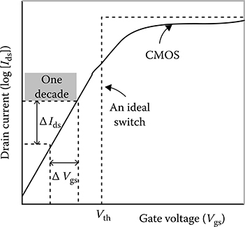
FIGURE 9.1 Subthreshold slope definition. CMOS subthreshold slope is 60–70 mV/decade. An ideal switch offers 0 mV/decade subthreshold slope.
The current projections by the International Technology Roadmap for Semiconductors (ITRS) show that the end of the road on metal–oxide–semiconductor FET (MOSFET) scaling will arrive sometime around 2022 with an 11 nm process [8]. Process variation and increasing fabrication costs have to be addressed before CMOS can be scaled further. In 20-nm CMOS, the gate oxide is only about five atoms thick. If merely a single atom is out of place, the gate-oxide thickness varies by 20%. This process variation will only worsen with scaling [8].
The single largest hurdle to further scaling of the MOSFET is the fabrication cost. The semiconductor industry might solve the fabrication cost hurdle to enable further scaling, given its track record. However, the physical size limitations and fabrication cost restrictions will require a paradigm shift in design of electronic circuits. Many devices are being explored for cointegration with CMOS technology to solve the above issues.
9.2 CMOS Replacement Devices: Mechanical Relays
Numerous emerging devices that offer better energy efficiency per operation that could potentially act as CMOS replacement devices have been proposed [8–12]. This list includes a plethora of emerging devices including, but not limited to, piezoelectric devices, magnetic devices, electrostatic devices, and carbon nanotube based devices. The fundamental limitation in CMOS is the trade-off between decreasing active energy and increasing leakage energy to get optimal energy efficiency. This trade-off requirement has to be eliminated to improve the energy efficiency of any emerging device. A mechanical switch with zero OFF state leakage exhibits this behavior. Pott et al. provide a comprehensive summary of history and advances in relay-based computing over the last decade [11]. Mechanical switches exhibit abrupt switching behavior that allows VDD to be decreased while maintaining relatively high ON state current. The use of mechanical switches (relays) for computing was first implemented in Zuse Z3—an electrically powered digital computer built in 1941. This computer used about 2000 relays to perform calculations for aircraft design [13]. Numerous advancements in planar processing technology over the past few decades have created a renewed interest in mechanical computing for ultralow power applications [11].
9.2.1 Electrostatically Actuated Nanoelectromechanical Relay Devices
MEMS technology has seen significant advances in the last decade and the electrostatic MEMS relay is by far the most common as it requires extremely low power and relatively straightforward fabrication requirements. Improvements in silicon fabrication techniques have allowed three-dimensional structures to be realized from silicon substrates. Numerous sensor and actuator circuits have been designed using MEMS technology. MEMS devices can be free-standing or can have one or more degrees of freedom. This freedom allows them to serve many different functions. The ability to design unique structures that implement the same functionality of CMOS transistors but without the drawbacks of transistor technologies is the key advantage of MEMS devices. Scaling MEMS relays down to the nanoscale to create fast, reliable, miniature nanoelectromechanical (NEM) relays is the logical next step for the MEMS relay technology as well. Numerous MEMS devices that operate similar to an ideal switch have been reported [14,15]. NEM devices actuated electrostatically are attractive for IC applications because they are relatively easy to manufacture using conventional planar processing techniques/materials, do not consume much active power, and are scalable. The device stress and actuation potential increase with reduction in feature size. Hence scaling of relays leads to better reliability and energy efficiency [5,8,16].
NEM relays are essentially three- or four-terminal mechanical switches that are electrostatically actuated. The channel could be metal or semiconductor channel (creates a field-effect transistor when the mechanical parts come in contact). The metal channel relays are more appealing than the semiconductor channel as the latter inherently has all the limitations of CMOS with respect to energy efficiency reduction. In a metal channel relay, when the mechanical switch is turned ON, the channel creates a conducting path between source and drain. When the switch is OFF, there is no drain-source current and hence, the leakage through the device is zero. The electrostatic actuation of the mechanical switch results in a mechanical delay in the relay, which far exceeds the electrical delay of the logic implemented using the relays.
NEMS devices offer another significant advantage over CMOS. As alluded to previously, CMOS circuits are susceptible to harsh and extreme operating conditions. However, NEM relays, being mechanical switches, offer fairly reliable operation in the presence of harsh and extreme operating conditions [17,18].
9.2.2 NEM Relay Devices
9.2.2.1 Cantilever Beam and Laterally Actuated NEM Relays
A cantilever beam–based NEM relay has been reported by Chen et al. [19]. This is the simplest and most intuitive mechanical switch that is electrostatically actuated. Figure 9.2 shows a cantilever beam relay [19]. This is a four-terminal device. The cantilever beam forms the gate terminal. The base terminal is below the beam. The gate carries a metal channel and contact dimples that touch the source and drain terminals below when the beam is actuated. So, when the relay is ON, it creates a metal channel between source and drain terminals through the contact dimples. When the relay is OFF, there is no drain-source current and hence, the leakage through the device is zero. Hence, the relay behaves similar to an ideal switch.
A laterally actuated NEM relay device is reported by Chong et al. [20], in which a polysilicon beam is laterally actuated to realize the mechanical switch. This relay has been heterogeneously integrated with CMOS technology to realize a hybrid NEMS–CMOS static random access memory (SRAM) cell, which showed improved bitcell stability and lower energy dissipation.
9.2.2.2 Suspended Gate Relays
A four-terminal suspended gate NEM relay devices has been reported [5], which incorporates a movable poly-SiGe gate suspended by spring-like folded flexures above tungsten electrodes. A thin coating of titanium oxide is applied to the device to improve the reliability of the suspended gate. Relays operating at 10 V with a 90-nm nominal gap between the dimples on drain/source and the suspended gate have been fabricated and reported. Spencer et al. also discuss a scaled relay operating at 1 V with a nominal gap of 5–10 nm between the gate and drain/source [5]. Figure 9.3 shows the device construction and basic electrical/mechanical elements in the relay circuit. Figure 9.4 shows the voltage transfer characteristics of the relay. The suspended gate is electrostatically actuated whenever there is a voltage between the gate and base. When the electrostatic force is strong enough to overcome the spring-mass-damper system, the channel electrode touches the dimples on source and drain, thereby creating a metal channel between source and drain. When the voltage between gate and base is lowered, the electrostatic force reduces and eventually will open the relay once it crosses a release threshold voltage. Since there is no metal channel between source and drain when the relay is off, there is no leakage current.
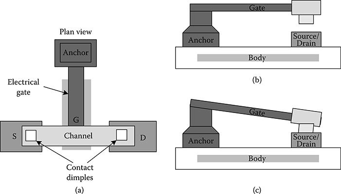
FIGURE 9.2 (a) Cantilever beam relay. (From Chen, F. et al., Integrated circuit design with NEM relays, 2008 IEEE/ACM International Conference on Computer-Aided Design [ICCAD]© 2008 IEEE.) (b) The nonactuated relay. (c) When actuated, the contact dimples touch source and drain terminals. (Reprinted with permission from R. Venkatasubramanian, S. K. Manohar, and P. T. Balsara, NEM relay-based sequential logic circuits for low-power design, IEEE Transactions on Nanotechnology, 12[3], © 2013 IEEE.)
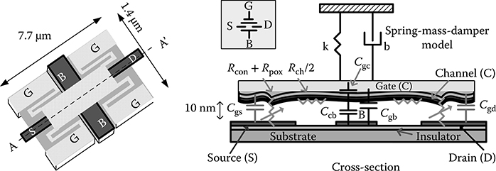
FIGURE 9.3 Suspended gate relay (From Spencer, M. et al., Demonstration of integrated micro-electro-mechanical relay circuits for VLSI applications, IEEE Journal of Solid-State Circuits, 46[1], © 2011 IEEE.) NEM Relay symbol shown in the inset. The cross-sectional view is along axis AA′ shown in the plan view. The suspended gate is modeled as a spring-mass-damper system. (Reprinted with permission from R. Venkatasubramanian, S. K. Manohar, and P. T. Balsara, NEM relay-based sequential logic circuits for low-power design, IEEE Transactions on Nanotechnology, 12[3], © 2013 IEEE.)
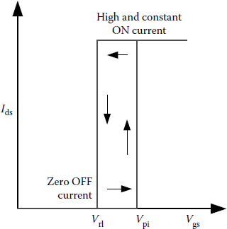
FIGURE 9.4 The voltage transfer characteristics of the relay.
9.3 Verilog-A Model of Suspended Gate Relay
9.3.1 Definition of NEM Relay Parameters
Pull-in voltage Vpi is the voltage applied between gate and base above which the electrostatic force overcomes the spring-mass-damper system and the relay turns ON. Release voltage Vrl is defined as the voltage below which the relay opens and the switch is OFF. The NEM relay exhibits a hysteretic property for the pull-in and release threshold voltages. The pull-in voltage (Vpi) is larger than the release voltage (Vrl). The mechanical delay involved in switching ON the relay is denoted as tmon and the mechanical delay involved in switching OFF the relay is denoted as tmoff. The mechanical delay is an order of magnitude larger than the electrical delay of the relay (te). As an example, the mechanical delay of the suspended gate relay used in this work is of the order of hundreds of nanoseconds, whereas the electrical delay is of the order of tens of picoseconds.
9.3.2 Electromechanical System Model
The electromechanical relay device is typically modeled as a spring-mass-damper system. Verilog-A model of the relay device is co-simulated with HSPICE [21] to simulate the second-order mechanical system defined in Equation 9.1 and the electrical model of the relay. This simulation comprehends all the mechanical and electrical effects involved in the electrostatic actuation of the relay in a circuit. The Verilog-A model covers the self-actuation effect but does not cover electro- or mechanical-thermal effects.
Dispersion forces such as Casimir and Van der Waals’ force strongly affect the mechanical behavior of nanoscale devices. In nanoscale devices, the effects of these two forces are so significant that they must be considered even in absence or presence of electrostatic forces. Hence, it is very important to factor these dispersion forces in the Verilog-A model of the NEM relay device.
An accurate Verilog-A model of the suspended gate relay operating at 1 V with a nominal air gap of 5–10 nm developed by Venkatasubramanian et al. [22] has been used to validate the circuits described in this chapter. At any instant in time, the electrostatic force (Felec) balances with the spring-mass-damper system.
As alluded to previously, in nanoscale electromechanical devices, dispersion forces such as the Casimir force and Van der Waals’ force affect the pull-in stability of the relay devices significantly [23,24]. Dispersion forces decrease the pull-in deflection and actuation voltage of the relay. However, the fringing field increases the pull-in deflection while decreasing the pull-in voltage (Vpi) of the relay. The model also accounts for the dispersion forces.
Van der Waals’ force is the dominant force of attraction when the air gap separation is below several tens of nanometers (nonretarded regime) [24]. If the air gap separation is above several tens of nanometers, the Casimir force is dominant. As the 1 V suspended gate relay has a separation well within tens of nanometers, the Casimir force is assumed to be negligible and hence Van der Waals’ force alone is considered in the relay model.
Hence, the force vector equation is expressed as follows:
where x is the displacement of the gate, m the mass of the suspended gate, k the spring constant of the gate structure, and b the damping coefficient of the motion of the gate.
The electrostatic force Felec is expressed as:
where ∈0 is the permittivity of free space, Vgb the voltage between gate and base, Aov the area of overlap between gate and base electrodes, and g0 is the normal gap between electrodes when switch is OFF.
The Van der Waals’ force per unit length ΔFvdW is given by:
where A is the Hamaker constant [24] (~1.6 eV for Si with no surface layer) and w the width of the suspended gate relay. The Hamaker constant, A, can be roughly defined as a material property that represents the strength of Van der Waals’ interactions between macroscopic bodies. It is defined in Joules. Typical values of A varies in the range of 10−19−10−20 J for various material bodies [25].
For two parallel and flat surfaces (as in the case of suspended gate relay), the total Van der Waals’ force of the suspended gate FvdW is expressed as:
where L is the length of the suspended gate relay. In the case of cantilever beam relays or laterally actuated relays, Equation 9.3 has to be integrated over the length of the relay, taking into account the bending effects of the beam to determine the total Van der Waals’ force. The impact of Van der Waals’ force on the pull-in parameters of cantilever beams is given in [26].
The voltage necessary to turn on the relay is the pull-in voltage and is derived to be as follows:
The mechanical delay (tm) is inversely proportional to the gate overdrive voltage (|Vgb|/Vpi) and the undamped angular frequency of the spring-mass-damper system [27]. This is denoted by
9.4 Nem Relay–Based Digital Logic Design
The speed of operation of a NEM relay–based digital logic circuit is limited by the mechanical delay of the switch. As the mechanical delay far exceeds the electrical delay of the switch, it has been proposed that combinatorial relay logic be implemented as complex gates to minimize the number of mechanical delays in the critical path [5,19]. It has been shown that relay logic offers up to 10× efficiency gain in low-frequency circuits (operating up to 100 MHz) by having multiple parallelized architectures to achieve a certain throughput [5,19]. To be able to build large digital logic circuits using relays, sequential and combinatorial logic circuits need to be realized, taking into account the device properties to minimize the mechanical delays in the critical paths.
9.4.1 Intrinsic Capacitance of the Relay (Cint)
In the cantilever beam relay and the suspended gate relay a true parallel plate capacitor exists between gate and base (Cgb). The small overlap area between gate and source/drain also creates small parallel plate capacitances Cgs and Cgd. It is reported in [5] that Cgb is of the order of 1–2 fF and contributes approximately 60% of the total relay self-capacitance. Because of the near-zero leakage in the relay, charge stored in these capacitors is retained very efficiently. This intrinsic capacitance could be used in relay-based circuit design.
9.4.1.1 Relay-Based Latch Circuits
9.4.1.1.1 Bootstrap Latch
The intrinsic capacitance of the relay is used to improve the latch performance in the bootstrap latch shown in Figure 9.5a. R2 and R3 form a buffer. Relay R4 essentially bypasses the buffer when CLK is high and provides a faster Q output. The output Q is available after one mechanical delay (tm). Note that R1 and R4 switch ON at the same time. The intrinsic capacitor is charged (in tm time), and either of the relays R2 or R3 turn ON depending on D being “1” or “0.” Note that R2 or R3, once turned ON, stay ON until the next cycle or whenever Cint is affected. Relay R4 electrically isolates the output when CLK = 0 and preserves the charge in Cint. This ensures that loading at the output Q does not affect the intrinsic capacitance Cint. Even though relays R2 and R3 take another tm delay to close, this is hidden from the CLK-Q delay of the latch.
Ideally, for bootstrapping functionality, we expect output Q to replenish the charge in the intrinsic capacitance Cint once the input is latched. So instead of relay R4, Q could be directly connected to the Cint node to make it a true bootstrapping latch. But the loading on output Q might discharge the intrinsic capacitance Cint and the latch might not be able to hold the value stored in it.
The operation of the latch is shown in Figure 9.5c. The mechanical displacement of the suspended gate with respect to the nonactuated OFF position of the relays R1 and R2 is shown in the waveform as well. When a relay R1 is OFF, R1.x_pos = 0. The CLK and D signals require a minimum pulse width of tm in order for the latch to be functional. The minimum setup time is the electrical delay te = Ron * Cint, where Ron is the ON resistance of the relay and Cint the intrinsic capacitance. The dead time for the minimum setup is Ron * Cint + tm. When D = 1, Q = 0, or D = 0, Q = 1, there is a possibility of drive fight when CLK = 1, and node dint could be corrupted. To minimize this drive fight, relay R1 should be sized stronger than R4. If R1 is constructed using two parallel relays, effective feedback resistance (Ron of R4) would be twice that of the setup path resistance (Ron of R1), thereby aiding the new value to be written into the flip–flop.
9.4.1.1.2 Keeper Latch
In the absence of an intrinsic capacitance (as in the case of the lateral actuation relay [20]), the performance of the latch can be improved using the classic back-to-back CMOS inverter topology optimized differently for NEM relays. The latch topology is shown in Figure 9.5b. Relay pairs R2–R3 and R4–R5 form buffers. The CLK-Q delay of this latch is 2tm (Relay R1 to turn ON, then the buffer R2–R3 to turn ON). The mechanical delay required to turn ON the relays in the recirculating path is hidden. The minimum setup time is the electrical delay te = Ron * Cint, where Ron is the ON resistance of the relay and Cint the intrinsic capacitance. The dead time for the minimum setup is Ron * Cint + 2 * tm. When D = 1, CLK = 1, and Q = 0, there is a direct path from D to ground through relays R1 and R5. Essentially, the relays will operate as a potential divider and node d_int will get a value of Vdd/2. If Vpi > Vdd/2, it will result in a setup failure and will make the latch circuit inoperable. Same condition applies for D = 0, CLK = 1, and Q = 1. To avoid the setup failure, multiple parallel relays could be added in the place of R1 (reduce the effective resistance) to ensure that node d_int has a swing above Vpi.
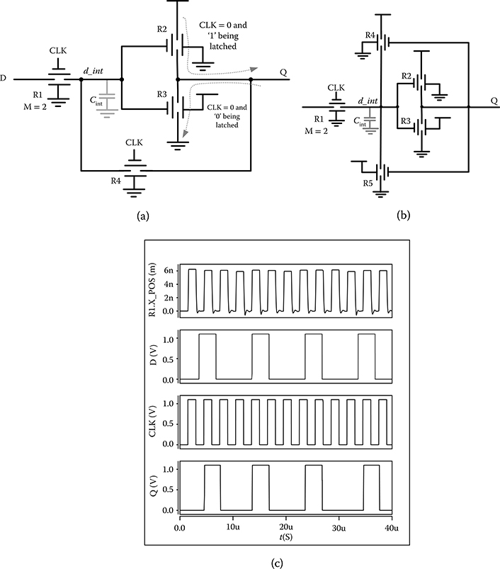
FIGURE 9.5 (a) Bootstrap latch, (b) keeper latch, and (c) bootstrap latch operation. (Reprinted with permission from R. Venkatasubramanian, S. K. Manohar, and P. T. Balsara, NEM relay-based sequential logic circuits for low-power design, IEEE Transactions on Nanotechnology, 12[3], © 2013 IEEE.)
9.4.1.2 Relay-Based Flop Circuits: Tristate Relay Flop
A flop using only four relays and operating at a frequency of 1/2tm has been proposed by Venkatasubramanian et al. [28]. The flip–flop topology is shown in Figure 9.6a. Relays R2 and R3 form a buffer. When the CLK is low, the intrinsic capacitance is charged and the buffer is turned ON. The latched value is available at the buffer output. When CLK turns high, the output gets the latched value after one mechanical delay (tm). Note that the base of R1 is connected to VDD. So R1 will turn ON when CLK is low. The operation of this flop is shown in Figure 9.6b. The mechanical displacement of the suspended gate with respect to the default position is shown in the waveform for relay R1. When R1 is OFF, R1.x_pos = 0.
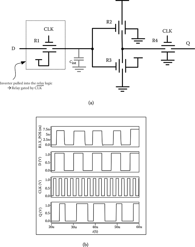
FIGURE 9.6 (a) Tristate flop, and (b) tristate flop operation. Both electrical and mechanical measurements are shown. R1.x_pos is the mechanical displacement of the suspended gate in the Y direction with respect to nonactuated position of the relay. (Reprinted with permission from R. Venkatasubramanian, S. K. Manohar, and P. T. Balsara, NEM relay-based sequential logic circuits for low-power design, IEEE Transactions on Nanotechnology, 12[3], © 2013 IEEE.)
9.4.1.3 Max Frequency of Operation and Min-Pulse Width
The clock and data signals of the sequential logic circuits should have a pulse width of at least tm for the logic operation to succeed. Care must be taken to ensure that this min-pulse width is guaranteed on all intermediate nodes of the relay logic circuit as well. This limits the maximum frequency of operation of a relay logic circuit to at most 1/2tm. The setup time, hold time, and the Tclk-Q delay for each of the sequential logic circuits proposed in this work is listed in Table 9.1. The electrical delay in each sequential circuit is denoted as te (= Ron * Cint). This work proposes a flop (tristate flop) and a latch (bootstrap latch) that can work at a frequency of 1/2tm—which is theoretically the fastest sequential circuit possible for a NEM relay logic circuit for a given nominal overdrive voltage |Vgb|/Vpi.
9.4.1.4 Performance, Energy, and Area Comparison
The performance and area (relay count) comparison between the various sequential logic topologies is shown in Table 9.1. The electrical delay in each circuit is denoted as te (= Ron * Cint). Setup time reported is the drop-dead setup time and CLK-Q delay reported is for infinite setup time—in line with the definition of setup and CLK-Q delay for CMOS circuits. For latch circuits, setup time is measured when the latch is getting disabled. In flip–flop circuits, setup time is measured at the rising edge of the clock. The tristate flop gives the maximum performance for the smallest area penalty. Among latches, the bootstrap latch gives the maximum performance as the tristate flop.
The Verilog-A model is co-simulated with HSPICE to prove the functional correctness of the sequential logic circuits and to obtain the energy per transition. The co-simulation comprehends all the mechanical and electrical effects involved in the electrostatic actuation of the relay in a circuit. The relay operates at 1 V with Vpi = 0.6 V, Vrl = 0.55 V, tmon = 130 nanoseconds. The average current Iavg, energy per transition for 0 to 1 transition (E0→1), and 1 to 0 transition (E1→0) are also reported for each of the sequential cells in Table 9.2.
Table 9.1 Performance Metrics of NEM Relay Sequential Circuits
Type |
No. of Relays (count) |
Setup Time |
Hold Time |
CLK-Q Delay |
Comment |
Bootstrapping Latch |
5 |
te |
0 |
tm Latch |
Fast |
Keeper latch Tristate |
6 |
te |
0 |
2tm |
Fastest flop |
Flop |
4 |
te |
0 |
tm |
For a given Voverdrive |
9.4.1.5 Improving Performance of NEM Relay Circuits Using Charge Boosting
As the speed of operation of NEM relay logic circuits is primarily limited by the mechanical delay, multiple circuit techniques are explored to improve the speed of operation of NEM relay logic circuits.
The suspended gate relay illustrated in this chapter has Vpi as approximately 0.6 V and the nominal operating voltage is 1 V. So the nominal gate overdrive voltage (|Vgb|/Vpi) = 1.66x. The mechanical delay (tm) is inversely proportional to the gate overdrive voltage (|Vgb|/Vpi) as shown in Equation 9.6. This is illustrated in Figure 9.7. tmoff does not vary as much with overdrive voltage for the suspended gate device used in this work. Charge boosting enables faster relay operation at the expense of the device reliability. So, as long as the device can handle an overdrive voltage reliably, this concept can be used to improve the mechanical delay of the relay. Metal engineering techniques can be used to improve the reliability of operation for overdriven relays. However, this might increase the relay fabrication cost.
A localized charge-boosting scheme to overdrive Vgb to improve the performance of the mechanical switch was first proposed by Venkatasubramanian et al. [29]. The parallel plate capacitance between the gate and base of the relay is significant enough and hence is used to realize the storage capacitance. The feasibility of localized charge boosting is tested out by integrating the charge-boosting logic into the tristate flop.
Table 9.2 NEM Relay Flops/Latches: Power/Energy Comparison
|
Iavg |
E0→1 |
E1→0 |
Sequential cell |
(A) |
(J) |
(J) |
Bootstrap latch |
1.19e-11 |
1.18e-16 |
2.63e-11 |
Tristate flop |
1.03e-15 |
2.43e-15 |
1.69e-16 |
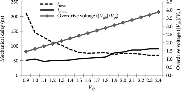
FIGURE 9.7 Mechanical delay (tmon, tmoff) versus overdrive voltage. For an overdrive of 2×, tmon reduces by approximately 2×. tmoff does not vary as much with overdrive voltage for the suspended gate model referred to in Section 9.3.
An integrated charge-boosting flip–flop using a cross-coupled voltage doubler is proposed by Venkatasubramanian et al. [28]. The doubler could be integrated with a single flip–flop or a group of flip–flops (vector flops) thereby minimizing the area overhead incurred for the doubler circuit.
9.4.1.5.1 NEM Voltage Doubler and Integrated Charge-Boosting Flip–Flop
It is important to recollect that the relay turns on whenever |Vgb| > Vpi. The operation of the relay for various gate/base voltage combinations is shown in Table 9.3.
A two-phase two relay cross-coupled voltage doubler shown in Figure 9.8a is used to generate differential signals X, X which swing between (Vdd, 2Vdd) [30]. A constant local supply of Vout = 2Vdd is generated as well. The operation of the doubler is shown in Figure 9.8b. Nonoverlapping two-phase clock is typically generated using break-before-make circuit [31].
The operation of the doubler is controlled by nonoverlapping clocks φ1 and φ2 and a set of delayed nonoverlapping clocks φ1d and φ2d. Relays Rc1 and Rc2 are configured in such a way that the parallel plate capacitor between the gate and the base terminals act as the fly capacitor (CFLY) for the doubler operation. Depending on the loading on the doubler circuit, multiple parallel relays are required to realize the total doubler capacitance. Relays R1 and R2 are turned ON on alternating phases of the clock and the relays Rc1 and Rc2 are charged to Vdd, respectively. Early clocks φ1 and φ2 set up the latch initially and thereby decouple the charging and discharging operations of the doubler. This also eliminates the short circuit current in the doubler altogether. The outputs X and X swing between Vdd and 2Vdd. Relays R3 and R4 along with multiple parallel relays Rc3 to realize the variable storage capacitor (CST) generate a constant local 2Vdd supply. This is shown in Figure 9.9b.
The NEM voltage doubler concept is extended to develop an integrated charge-boosting flip–flop and is described in detail by Venkatasubramanian et al. [29]. Basically, the integrated charge-boosting flip–flop that deploys localized charge boosting should provide the following:
Rail-to-rail output swing of [0, 2Vdd]
Reduce mechanical delay of operation to tm/2
Table 9.3 NEM Relay Operation for Various Vg/Vb Combinations
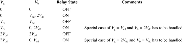
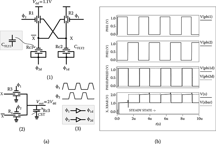
FIGURE 9.8 (a) NEM voltage doubler that uses relays for storage capacitance, and (b) NEM voltage doubler operation. (Reprinted with permission from R. Venkatasubramanian, S. K. Manohar, and P. T. Balsara, NEM relay-based sequential logic circuits for low-power design, IEEE Transactions on Nanotechnology, 12[3], © 2013 IEEE.)
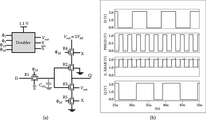
FIGURE 9.9 (a) Integrated charge-boosting flip–flop. (b) Operation. (Reprinted with permission from R. Venkatasubramanian, S. K. Manohar, and P. T. Balsara, NEM relay-based sequential logic circuits for low-power design, IEEE Transactions on Nanotechnology, 12[3], © 2013 IEEE.)
9.4.5.1.2 Integrated Charge-Boosting Flip–Flop Design
The integrated charge-boosting flip–flop is shown in Figure 9.9a and the timing diagram for the operation of the flip–flop is shown in Figure 9.9b. Note that D is assumed to be swinging between [0,2Vdd] as the previous flop (or) a primary input (PI) would be driving it with this larger swing. As the swing of D is [0, 2Vdd], this overdrive voltage gets applied to relays R2 and R3 and they turn ON faster. Relay R1, which samples D on the negative edge of the clock, is controlled by φ1d and X. The constant local supply voltage of 2Vdd is supplied by the doubler. Relays R4 and R5 are sampled by differentially overdriven clock φ2d and X. The latched value of D is sampled on the positive edge of the system clock (φ1d).
9.5 Nem Relay–Based Memory Design
Memories are important elements in electronic circuit design and a few interesting relay-based memory architectures have been reported. The bistable seesaw relay device described by Jeon et al. [32] has been proposed for use as a memory cell with one seesaw relay and one access transistor. A suspended relay–based memory architecture has been proposed by Gupta [33]. A multivalued memory architecture using relays has been proposed by Stalter [34]. Three new parallel readout bitcell architectures are proposed by Venkatasubramanian et al. [35], which address the limitations of Gupta [33] and simultaneously improve the memory access time.
9.5.1 Three-Relay Random Access Memory (3RRAM)
A three-relay RAM (RRAM) architecture proposed by Gupta [33] has three-relay devices in each bitcell. The memory architecture is shown in Figure 9.10a. Each bitline has a global precharge circuitry. The intrinsic capacitance of the relay (Cint) is used to store the charge in each bitcell. The fundamental limitation of this architecture is that the readout is serial in nature. Data stored in word “0” is accessible only if all the other words (words 1…n) are enabled, and so on.
9.5.2 Two-Relay Random Access Memory (2RRAM)
A two-relay bitcell with an external capacitor has been proposed by Gupta [33] and is shown in Figure 9.10b. This architecture has the serial readout limitation as well. In addition, an external capacitance is assumed for charge storage.
As both of the above bitcell architectures implement serial readout, they have higher read access time (RAT). Further, as each bitcell read involves all the bitcells in the memory array column, this poses a reliability issue in the memory operation. The entire column becomes nonfunctional even if one of the bits in that column is not reliable. Also, serial readout architecture is not conducive for low-voltage operation because of their higher voltage headroom requirements.
9.5.3 P4RRAM: Parallel 4R RAM Bitcell
P4RRAM—Parallel 4R RAM bitcell is based on the tristate flop topology (Figure 9.6). The bitcell architecture is shown in Figure 9.11a.
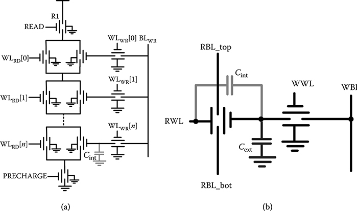
FIGURE 9.10 (a) 3RRAM memory bitcell and memory architecture, and (b) 2RRAM memory bitcell.
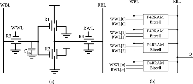
FIGURE 9.11 (a) P4RRAM Bitcell. (b) P4RRAM Array Column.
Tristate flop operation is explained in Section 9.4.1.2. Relays R1 and R2 form a buffer. When the CLK is low, the intrinsic capacitance is charged and the buffer is turned ON. The latched value is available at the buffer output. When CLK turns high, the output gets the latched value after one mechanical delay (tm). This concept is used in the topology of the P4RRAM bitcell. As it is a parallel readout architecture, the read bitline (RBL) can be shared across all the bitcells in the column and can be tristated when there is no read operation. No precharge or predischarge of RBL is necessary.
This memory bitcell is very reliable as it stores both “1” and “0” and drives the output directly from the supply. Also, the RAT is one mechanical delay (tm) for both the read and write operations. The memory array column for this bitcell is shown in Figure 9.11b.
As long as the RC delay required to discharge the RBL capacitance is less than one mechanical delay, additional sense amplifier circuitry is not required to improve the RAT.
9.5.4 P3RRAM: Parallel 3R Ram Bitcell
P3RRAM bitcell (Parallel 3R RAM) is a variant of the 4R bitcell described in Section 9.5.3, in which zero storage capability has been removed to minimize the bit-cell area. The bitcell architecture is shown in Figure 9.12a. Hence, the memory RBL has to be predischarged before every read operation. This results in additional delay for the RAT. The memory array column for this bitcell is shown in Figure 9.12b.
The basic read operation of this bitcell is shown in Figure 9.13a. Bit[0] is storing a “0” and Bit[1] is storing a “1.” The predischarge cycle before every read operation ensures that the RBL is discharged. When Bit[1] is read out by asserting RWL[1], the RBL gets asserted to “1.”
9.5.5 P3RRAM-SNR
This bitcell topology proposes a notion of storage node refresh (SNR) where the bit-cell state is replenished through the write bitline every time a memory write operation is performed. The bitcell architecture is shown in Figure 9.13b. An external capacitance C1 is added to each bitcell and it holds the state of the bitcell and facilitates faster readout. The circuit topology ensures that the internal capacitance C1 is replenished and the bitcell state is preserved during any memory write operation. Charge replenishment enables a reliable memory operation and also improves the memory RAT.
9.5.6 Comparison of the NEM Relay Bitcell Architectures
The low- and high-noise margins (NML and NMH, respectively) for a relay circuit can be defined by examining the DC transfer characteristic of a relay-based buffer [33]. The DC characteristics of a buffer are shown in Figure 9.14.
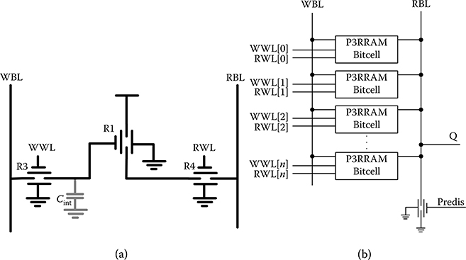
FIGURE 9.12 (a) P3RRAM Bitcell. (b) P3RRAM Array Column.
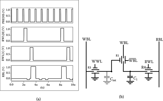
FIGURE 9.13 (a) P3RRAM Bitcell operation. (b) P3RRAM-SNR Bitcell.
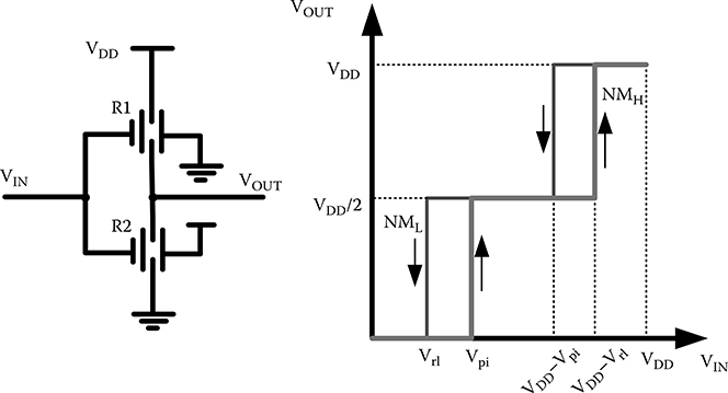
FIGURE 9.14 Relay buffer (left) and its DC transfer characteristics (right).
The write margin, read margin, and hold margin of a memory bitcell are the key metrics that define the stability and noise tolerance characteristics of the bit-cell. For each of the bitcell architectures proposed, the margin metrics are shown in Table 9.4.
The relay parameters used in Table 9.4 are as follows:
tm: the mechanical switching delay
Ron: ON resistance of the relay
Cint: the intrinsic capacitance of the relay
C1: the external capacitance added in P3RRAM-SNR
CRBL: the capacitance of the RBL
The electrical delay in each of the bitcell circuits is a function of the relay ON resistance Ron and the capacitance involved in charge storage. The advantages and disadvantages of each of the bitcell architectures are shown in Table 9.5.
Stability metrics: Write margin is the maximum noise that the bitcell can handle during a write operation without corrupting the value being stored. Read margin is the maximum noise that the bitcell can handle that will not corrupt the value stored in the memory during a read operation. Hold margin is a measure of the data retention property of the bitcell and is defined as the noise voltage above which the bitcell will fail to hold the value, thereby corrupting the memory location.
Performance metrics: RAT, write access time (WAT), and cycle time (Tcc) are the typical performance care-abouts for a memory bitcell. The comparison of various performance metrics and stability metrics is shown in Table 9.4.
Table 9.4 Performance/Stability Metrics for the Bitcell Architectures
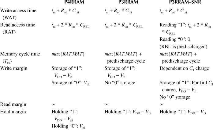
Table 9.5 Summary of NEM Relay–Based Memory Bitcell Architectures
In summary, the P3RRAM bitcell offers a good compromise between area, speed, and reliability among all the NEM-relay bitcell architectures. The P3RRAM-SNR bitcell provides faster RAT with an additional external capacitor.
9.6 Conclusion
Over the past few decades, CMOS technology scaling has enabled constant reduction of energy-per-operation in integrated circuits. But the threshold voltage of the transistors has already been scaled to its limit and any further reduction in the threshold voltage would actually increase the amount of energy consumed per operation. So the need for new devices with steeper subthreshold slope such as NEM relay is necessary to enable further reduction of energy-per-operation in integrated circuits. To be able to build large logic circuits using NEM relays, the key building blocks such as combinatorial logic, sequential logic, SRAMs, and IOs need to be studied in detail. This chapter gives an overview of two of the key building blocks of NEM relay logic—sequential latch and flip–flops have been shown to have a delay of 1/2tm, which is theoretically the fastest frequency possible for a given overdrive voltage.
According to ITRS-2009 Emerging Research Devices report [36], “Approaches to minimize switching energy in which mechanical energy is stored and released to assist the transition between logic states merit further development (in NEM relays).” Several innovative circuits related to relay-based circuit architecture have been reviewed in this chapter. Conceivably, these circuits could form a relay logic–based cell library that could be used to build large-scale electronic circuits using NEM relays or NEMS–CMOS heterogeneous integrated circuits.
References
1. The International Technology Roadmap for Semiconductors (ITRS), 2011. http://public.itrs.net.
2. N. S. Kim, T. Austin, D. Baauw, T. Mudge, K. Flautner, J. S. Hu, M. J. Irwin, M. Kandemir, and V. Narayanan. Leakage current: Moore’s law meets static power. Computer, 36(12): 68–75, 2003.
3. D. Markovic, V. Stojanovic, B. Nikolic, M. A. Horowitz, and R. W. Brodersen. Methods for true energy-performance optimization. IEEE Journal of Solid-State Circuits, 39(8): 1282–1293, 2004.
4. H. Kam. MOSFET Replacement Devices for Energy-Efficient Digital Integrated Circuits. PhD thesis, University of California, Berkeley, CA, 2010.
5. M. Spencer, F. Chen, C. C. Wang, R. Nathanael, H. Fariborzi, A. Gupta, Hei Kam et al. Demonstration of integrated micro-electro-mechanical relay circuits for VLSI applications. IEEE Journal of Solid-State Circuits, 46(1): 308–320, 2011.
6. B. Nikolic. Design in the power-limited scaling regime. IEEE Transactions on Electron Devices, 55(1): 71–83, 2008.
7. W. M. Reddick and G. A. J. Amaratunga. Silicon surface tunnel transistor. Applied Physics Letters, 67(4): 494–496, 1995.
8. M. Haselman and S. Hauck. The future of integrated circuits: A survey of nanoelectronics. Proceedings of the IEEE, 98(1): 11–38, 2010.
9. Advanced CMOS and Emerging Technologies—Sematech, 2012. http://www.sematech.org/meetings/archives/symposia/9105/Jammy_Raj.pdf.
10. R. Jammy. Materials, Process and Integration Options for Emerging Technologies. Technical report, SEMATECH, 2009.
11. V. Pott, H. Kam, R. Nathanael, J. Jeon, E. Alon, and T.-J. K. Liu. Mechanical computing redux: Relays for integrated circuit applications. Proceedings of the IEEE, 98(12): 2076–2094, 2010.
12. The Economist. New transistors: Mechanical advantage, July 15, 2011, p. 82, 2011. www.economist.com/node/18956106.
13. T.-J. K. Liu, E. Alon, V. Stojanovic, and D. Markovic. The relay reborn. IEEE Spectrum, 49(4): 40–43, 2012.
14. P. M. Zavracky, S. Majumder, and N. E. McGruer. Micromechanical switches fabricated using nickel surface micromachining. Journal of Microelectromechanical Systems, 6(1): 3–9, 1997.
15. D. A. Czaplewski, G. A. Patrizi, G. M. Kraus, J. R. Wendt, C. D. Nordquist, S. L. Wolfley, M. S. Baker, and M. P. de Boer. A nanomechanical switch for integration with CMOS logic. Journal of Micromechanics and Microengineering, 19(8): 085003, 2009.
16. H. Kam, V. Pott, R. Nathanael, J. Jeon, E. Alon, and T. -J. K. Liu. Design and reliability of a micro-relay technology for zero-standby-power digital logic applications. In 2009 IEEE International Electron Devices Meeting (IEDM), pp. 1–4, Baltimore, MD, 2009.
17. X. Wang, S. Narasimhan, S. Paul, and S. Bhunia. NEMTronics: Symbiotic integration of nanoelectronic and nanomechanical devices for energy-efficient adaptive computing. In 2011 IEEE/ACM International Symposium on Nanoscale Architectures (NANOARCH), pp. 210–217, San Diego, CA, 2011.
18. H. F. Dadgour. Evolutionary and Disruptive Approaches for Designing Next-Generation Ultra Energy-Efficient Electronics. PhD thesis, University of California, Santa Barbara, CA, 2010.
19. F. Chen, H. Kam, D. Markovic, T.-J. K. Liu, V. Stojanovic, and E. Alon. Integrated circuit design with NEM relays. In 2008 IEEE/ACM International Conference on Computer-Aided Design (ICCAD), pp. 750–757, San Jose, CA, 2008.
20. S. Chong, K. Akarvardar, R. Parsa, J.–B. Yoon, R. T. Howe, S. Mitra, and H.-S. P. Wong. Nanoelectromechanical (NEM) relays integrated with CMOS SRAM for improved stability and low leakage. In IEEE/ACM International Conference on Computer-Aided Design—Digest of Technical Papers (ICCAD) 2009, pp. 478–484, San Jose, CA, 2009.
21. HSPICE. User Guide: Simulation and Analysis, 2010.
22. R. Venkatasubramanian. Energy efficient circuit design using Nanoelectromechanical relays. PhD thesis, Department of Electrical Engineering, University of Texas, Dallas, TX, 2012.
23. R. Soroush, A. Koochi, A. S. Kazemi, A. Noghrehabadi, H. Haddadpour, and M. Abadyan. Investigating the effect of Casimir and van der Waals attractions on the electrostatic pull-in instability of nano-actuators. Physica Scripta, 82(4): 045801, 2010.
24. R. Maboudian and R. T. Howe. Critical Review: Adhesion in surface micromechanical structures. Journal of Vacuum Science Technology B: Microelectronics and Nanometer Structures, 15(1): 1–20, 1997.
25. J. N. Israelachvili. Intermolecular and Surface Forces, Revised 3rd Edition. Academic Press, Elsevier Science, USA, 2011.
26. A. Ramezani, A. Alasty, and J. Akbari. Influence of van der Waals force on the pull-in parameters of cantilever type nanoscale electrostatic actuators. Microsystem Technologies, 12: 1153–1161, 2006.
27. W.-C. Chuang, H.-L. Lee, P.-Z. Chang, and Y.-C. Hu. Review on the modeling of electrostatic MEMS. Sensors, 10(6): 6149–6171, 2010.
28. R. Venkatasubramanian, S. K. Manohar, and P. T. Balsara. NEM relay-based sequential logic circuits for low-power design. IEEE Transactions on Nanotechnology, 12(3): 386–398, 2013.
29. R. Venkatasubramanian, S. K. Manohar, and P. T. Balsara. Improving performance of NEM relay logic circuits using integrated charge-boosting flip flop. In 2011 IEEE/ACM International Symposium on Nanoscale Architectures (NANOARCH), pp. 37–44, San Diego, CA, 2011.
30. F. Pan and T. Samaddar. Charge Pump Circuit Design. McGraw-Hill electronic engineering series. McGraw-Hill, USA, 2006.
31. R. Venkatasubramanian, S. K. Manohar, and P. T. Balsara. Ultra low power high efficiency charge pump design using NEM relays. In 2011 IEEE 54th International Midwest Symposium on Circuits and Systems (MWSCAS), pp. 1–4, Seoul, South Korea, 2011.
32. J. Jeon, V. Pott, H. Kam, R. Nathanael, E. Alon, and T.-J. K. Liu. Seesaw relay logic and memory circuits. Journal of Microelectromechanical Systems, 19(4): 1012–1014, 2010.
33. A. Gupta. NEM Relay Memory Design. Master’s thesis, University of California, Berkeley, CA, 2009.
34. D. T. Stalter. Digital Logic and Multi-Valued Memory Using NEMS Switches. Master’s thesis, Case Western Reserve University, Cleveland, OH, 2010.
35. R. Venkatasubramanian, S. K. Manohar, V. Paduvalli, and P. T. Balsara. NEM relay based memory architectures for low power design. In 12th IEEE Conference on Nanotechnology (IEEE-NANO), 2012, pp. 1–5, Birmingham, England, 2012.
36. Emerging Research Devices. International Technology Roadmap for Semiconductors, 2009 edition. http://www.itrs.net/links/2009ITRS/2009Chapters_2009Tables/2009_ERD.doc, 2009.