
11 Basics, Applications, and Design of Reversible Circuits
Robert Wille
Contents
11.2 Basics on Reversible Circuits
11.3.2 Mapping Reversible Circuits to Quantum Circuits
11.4.2 Reversible Circuits in the Design of Low-Power Encoders
11.5 Design of Reversible Circuits
11.5.1 Considering the Number of Circuit Lines
11.1 Introduction
Great progress has been made in the development of computing machines. Over the last 20–30 years, a design flow was developed that allows for the specification and implementation of circuits and systems that are composed of millions of components. To handle the steadily increasing complexity, several abstractions are thereby applied during the design process—represented, for example, by the specification level, the electronic system level (ESL), the register transfer level (RTL), and the gate level. Here, the design of circuits and systems based on conventional computation paradigms has been focused.
However, conventional technologies are going to face serious challenges in the near future. The ongoing miniaturization (according to Moore’s Law), one of the main drivers of the last accomplishments in circuit and system design, eventually will come to a halt. At least when feature sizes of single transistors approach the atomic scale, no further improvement can be expected. Besides that, power dissipation represents a major obstacle. In the last decades, the amount of power dissipated in the form of heat to the surrounding environment of a chip increased by orders of magnitude. As excessive heat may decrease the reliability of a chip (or even destroys it), power dissipation is one of the major barriers to progress the development of smaller and faster computer chips. As a consequence, researchers and engineers are intensely considering alternative technologies.
Reversible computation marks a promising new computing paradigm where all operations are performed in an invertible manner. That is, in contrast to the conventional paradigm, all computations can be reverted (i.e., the inputs can be obtained from the outputs and vice versa). A simple standard operation such as the logical AND already illustrates that reversibility is not guaranteed in conventional systems. Indeed, it is possible to obtain the inputs of an AND gate if the output is set to 1 (then both inputs must be set to 1 as well). But, it is not possible to determine the input values if the AND outputs 0. In contrast, reversible computation allows bijective operations only, that is, n-input n-output functions that map each possible input vector to a unique output vector.
In this chapter, promising applications of this alternative computation paradigm are briefly reviewed. More precisely, we show how reversible circuits help in the design of quantum circuits—an emerging technology that makes it possible to solve many practically relevant problems much faster than conventional solutions. Besides that, possible benefits in the domain of low-power design are discussed, for example, a recent achievement in the design of low-power encoders where reversible circuits have successfully been applied. Afterwards, differences in the design of this kind of circuits are discussed and the current state of the art of the respective design methods is outlined. However, first, the most important basics on the reversible computation paradigm are provided.
11.2 Basics on Reversible Circuits
Logic computations can be defined as a function over Boolean variables. More precisely: A Boolean function is a mapping with n∈N. A function f is defined over its primary input variables X = {x1,x2,…,xn} and hence is also denoted by f (x1,x2,…,xn). The precise mapping is described in terms of Boolean expressions that are formed over the variables from X and operations such as ∧ (AND), ∨ (OR), or (NOT).
A multi-output Boolean function is a mapping with n, m ∈ N. More precisely, it is a system of Boolean functions fi (x1,x2,…,xn) with 1 ≤ i ≤ m. The respective functions fi are also denoted as primary outputs.
Multi-output functions are also denoted as n-input, m-output functions or n × m functions, respectively. Reversible functions are a subset of multi-output functions. More precisely, a multi-output function is reversible if:
Its number of inputs is equal to the number of outputs (i.e., n = m).
It maps each input pattern to a unique output pattern.
In other words, each reversible function is a bijection that performs a permutation of the set of input patterns. A function that is not reversible is termed irreversible.
Table 11.1 Boolean Functions
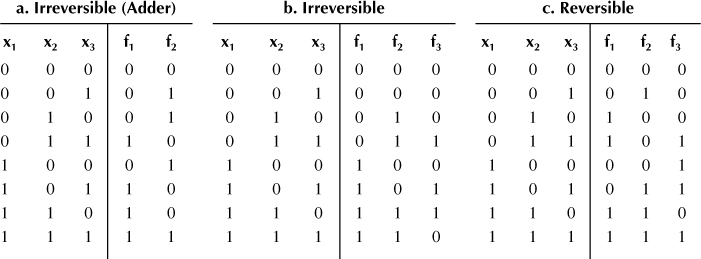
Table 11.1a shows the truth table of a three-input, two-output function representing a 1-bit adder. This function is irreversible, as n ≠ m. Also, the function in Table 11.1b is irreversible. Here, the number n of inputs indeed is equal to the number m of outputs, but there is no unique input–output mapping (e.g., both inputs 000 and 001 map to the output 000). In contrast, the 3 × 3 function shown in Table 11.1c is reversible, as each input pattern maps to a unique output pattern.
Reversible functions are realized by reversible circuits. A reversible circuit G is a cascade of reversible gates, where fanout and feedback are not directly allowed [1]. A reversible gate has the form g (C;T), where C = {xi1,…,xik} ⊂ X is the set of control lines and T = {xj1,…,xjl} ⊂ X with C∩T = ; is the set of target lines. C may be empty. Control lines and unconnected lines always pass through the gate unaltered. In contrast, the gate operation is applied on the target iff all control lines are assigned to 1. The most frequently used reversible gate is the Toffoli gate [2], which inverts the value of the (single) target line in this case.
Figure 11.1a shows a Toffoli gate drawn in standard notation, that is, control lines are denoted by •, whereas the target line is denoted by ⊕. A circuit composed of several Toffoli gates is depicted in Figure 11.1b. This circuit maps, for example, the input 111 to the output 110 and vice versa.
11.3 Quantum Computation
11.3.1 General Background
Quantum computation [1] is a promising application of reversible logic. Here, information is represented in terms of qubits instead of bits. In contrast to Boolean logic, qubits do not only allow the representation of Boolean 0s and Boolean 1s but also the superposition of both. In other words, a qubit is a two-level quantum system, described by a two-dimensional complex Hilbert space. The two orthogonal quantum states
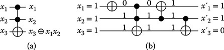
FIGURE 11.1 (a) Toffoli gate and (b) Toffoli circuit.
The state of a quantum system with n > 1 qubits is given by an element of the tensor product of the respective state spaces and can be represented as a normalized vector of length 2n, called the state vector. The state vector is changed through multiplication of appropriate 2n × 2n unitary matrices. Thus, each quantum computation is inherently reversible, but manipulates qubits rather than pure logic values.
Using quantum computation and qubits in superposition, functions can be evaluated with different possible input assignments in parallel. Unfortunately, it is not possible to obtain the current state of a qubit. Instead, if a qubit is measured, either 0 or 1 is returned depending on a respective probability, that is, 0 is returned 0 with probability of |α|2 and 1 is returned with probability of |β|2. After the measurement, the state of the qubit is destroyed.
Nevertheless, using these quantum mechanical phenomena, quantum computation allows for breaching complexity bounds which are valid for computing devices based on conventional mechanics. The Grover search [3] and the factorization algorithm by Shor [4] rank among the most famous examples for quantum algorithms that solve problems in time complexities, which cannot be achieved using conventional computing. The first algorithm addresses thereby the search of an item in an unsorted database with k items in time , whereas conventional methods cannot be performed using less than linear time. Shor’s algorithm performs prime factorization in polynomial time, that is, the algorithm is exponentially faster than its best known conventional counterpart. First physical realizations of quantum circuits have been presented in the work of Vandersypen et al. [5].
11.3.2 Mapping Reversible Circuits to Quantum Circuits
Reversible circuits are of interest in the domain of quantum computation as all quantum operations inherently are reversible. As most of the known quantum algorithms include a large Boolean component (e.g., the database in Grover’s search algorithm and the modulo exponentiation in Shor’s algorithm), the design of these components is often conducted by a two-stage approach: (1) realizing the desired functionality as a reversible circuit, and (2) mapping the resulting circuit to a functionally equivalent quantum circuit.
Different libraries of quantum gates have thereby been introduced for this purpose. In the literature, the NCV gate library [6] is frequently applied. This library is composed of the following universal set of quantum gates:
NOT gate : A single qubit t is inverted which is described by the unitary matrix .
ControlledNOT (CNOT) gate T ({c},t): The target qubit t is inverted if the control qubit c is 1.
ControlledV gate V ({c},t): The operation described by the unitary matrix is performed on the target qubit t if the control qubit c is 1.
ControlledV+ gate V+({c},t): The operation described by the unitary matrix is performed on the target qubit t if the control qubit c is 1. The V+ gate performs the inverse operation of the V gate as V+ = V−1.
The V and V+ gates often are referred to as controlled square-root-of-NOT gates as two adjacent identical V, or V+, gates are equivalent to a CNOT gate.
If circuits with Boolean inputs use NCV gates only, the value of each qubit at each stage of the circuit is restricted to one of {0,v0,1,v1} where and . The NOT, V, and V+ operations over these four-valued logic are given by:
x |
NOT (x) |
V (x) |
V+(x) |
0 |
1 |
v0 |
v1 |
v0 |
v1 |
1 |
0 |
1 |
0 |
v1 |
v0 |
v1 |
v0 |
0 |
1 |
As shown, NOT is a complement operation, V is a cycle, and V+ is the inverse cycle.
An alternative library has recently been introduced by Sasanian et al. [7]. Here, four-valued quantum gates are considered and summarized to the NCV-4 gate library. The NCV-4 gate library is composed of (1) the three unitary gates (i.e., gates without a control line) performing the NOT-, V-, and V+-operation as well as (2) respective controlled versions of these gates. In contrast to the NCV-library, the controlled gates perform the respective operation not in case the control line is 1, but in case the control line is set to the highest logic value (v1 in this case).
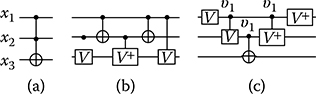
FIGURE 11.2 Mapping a Toffoli gate to respective quantum gates. (a) A Toffoli gate T ({x1,x2},x3), (b) to a functionally equivalent quantum circuits composed of NCV gates, and (c) NCV-4 gates.
Quantum circuits composed of gates from both libraries can easily be derived from reversible circuits. For this purpose, each reversible gate simply has to be mapped to a corresponding cascade of quantum gates. As an example, Figure 11.2 shows the mapping of (a) a Toffoli gate T ({x1,x2},x3), (b) to a functionally equivalent quantum circuits composed of NCV gates, and (c) NCV-4 gates, respectively. Improved mappings for other configurations of reversible gates or entire reversible circuits are available in the works of Barenco et al. [6], Miller et al. [8], and Soeken et al. [9].
11.4 Low-Power Design
11.4.1 General Background
Pioneering work by Landauer [10] showed that, regardless of the underlying technology, losing information during computation causes power dissipation. More precisely, for each lost bit of information, at least k · T · log (2) joules are dissipated (where k is the Boltzmann constant and T is the temperature). Since today’s computing devices are usually built of elementary gates such as AND, OR, NAND, and so on, they are subject to this principle and, hence, dissipate this amount of power in each computational step.
Although the theoretical lower bound on power dissipation still does not constitute a significant fraction of the power consumption of current devices, it nonetheless poses an obstacle for the future. Figure 11.3 illustrates the development of the power consumption of an elementary computational step in recent and expected future CMOS generations (based on values from the work of Zeitzoff and Chung [11]). The figure shows that today’s technology is still a factor of 1000 away from the Landauer limit and that the expected CMOS development will reduce this to a factor of 100 within the next 10 years. However, a simple extrapolation also shows that the trend cannot continue with the current family of static CMOS gates as no amount of technological refinement can overcome the Landauer barrier. Moreover, the Landauer limit is only a lower bound on the dissipation. Gershenfeld has shown that the actual power dissipation corresponds to the amount of power used to represent a signal [12], that is, Landauer’s barrier is closer than immediately implied by the extrapolation from Figure 11.3.
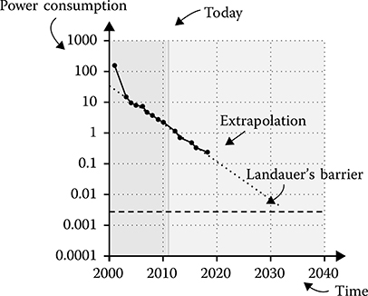
FIGURE 11.3 Power consumption Q in different CMOS generations.
As reversible circuits bijectively transforms data at each computation step, the above-mentioned information loss and its resulting power dissipation does not occur. Because of this, reversible circuits manifest themselves as the only way to break this fundamental limit. In fact, it has been proven that to enable computations with no power consumption at all, the underlying realization must follow reversible computation principles [13]. These fundamental results together with recent experimental evaluations [14] motivate researchers in investigating this direction further.
11.4.2 Reversible Circuits in the Design of Low-Power Encoders
A precise application of reversible circuits within the domain of low-power design can be found in the design of encoders for on-chip interconnects. With the rise of very deep submicron and nanometric technologies, these interconnects are increasingly affecting the overall energy consumption in today’s chips [15]. An established method to address this includes the application of coding strategies to modify the communication of the interconnects and, thus, to reduce the energy consumption [16,17].
The idea behind this is briefly illustrated by means of the probability based mapping (pbm) [16]. Here, it is assumed that the power consumption of the interconnect is related to the number of 1s transmitted through it. Hence, the pbm scheme tries to minimize the transmission of patterns with a large Hamming weight: Instead of transmitting the original data, each pattern is encoded depending on its probability.
As an example, Table 11.2a shows a set of data inputs with their corresponding probability of occurrence. Based on that, an encoder should map the most frequently occurring data input (i.e., 100) to a bit string with the lowest Hamming weight (i.e., 000). Then, the second-most frequently occurring data inputs should be mapped to a bit string with the second-lowest Hamming weight and so on. That is, a coding is desired, which leads to patterns with Hamming weights as shown in Table 11.2b. A precise coding satisfying this property is given in Table 11.2c.
Table 11.2 Illustrating the Objective of an Encoder
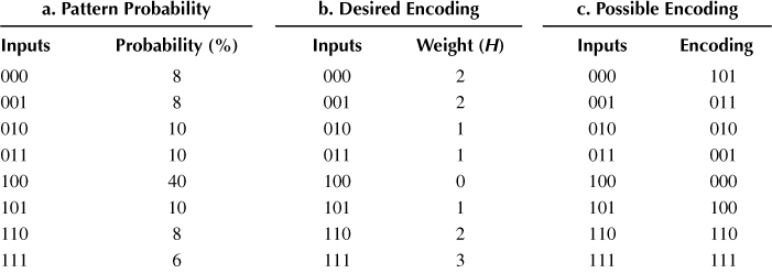
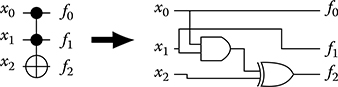
FIGURE 11.4 Mapping Toffoli gate to conventional circuit.
Unfortunately, determining the best possible or even just one good coding is a nontrivial task. Already for 3-bit data inputs as considered in Table 11.2a, eight different codings are possible. In the general case with m-bit data inputs, this number significantly increases to .
However, as encoders realize reversible one-to-one mappings, the application of synthesis approaches for reversible logic is a reasonable choice. In fact, the underlying reversibility of existing design methods for reversible circuits (see Section 11.5) enables to determine the desired codings in a more elegant and powerful way than their conventional counterparts. As the resulting reversible circuits represent a logic description, they can also easily be mapped to a conventional gate library. As an example, Toffoli gates with two control lines can be mapped to a netlist composed of one AND-gate and one XOR-gate as shown in Figure 11.4. From such a netlist, the established optimization and technology mapping steps can be performed.
11.5 Design of Reversible Circuits
The basics and the applications for reversible circuits as introduced in Sections 11.2, 11.3, and 11.4 already represent the main models and motivation for research in the domain of reversible circuit design. Nevertheless, reversible circuits have not been intensively studied by researchers before the year 2000. The main reason for that may lie in the fact that applications of reversible logic have been seen as “dreams of the future.” But, this changed as first physical realizations of reversible circuits emerged, that is, in terms of quantum circuits [5] or in terms of reversible CMOS realizations with certain low-power properties [18]. Therewith, proofs of concept were available motivating reversible circuits as a promising research area.
As a consequence, in the last years, researchers started to develop new methods for the design of this kind of circuits. In the following, the current state of the art is briefly reviewed.
11.5.1 Considering the Number of Circuit Lines
To synthesize compact reversible circuits, the number of used circuit lines is crucial—in particular for applications in the domain of quantum computation (see Section 11.3). Here, each circuit line corresponds to a qubit—a limited resource. Besides that, a large number of lines may decrease the reliability of the resulting system. For this, the number of circuit lines (or qubits) has to be kept as small as possible. However, often additional circuit lines are inevitable.
The following observations are thereby applied: If the function f : Bn → Bn to be synthesized is reversible, then obviously only n circuit lines are needed. In contrast, if irreversible functions are synthesized, additional lines might be required.
As an example, consider again the adder function from Table 11.1a. The adder obviously is irreversible, because (1) the number of inputs differs from the number of outputs, and (2) there is no unique input–output mapping. Even adding an additional output to the function (leading to the same number of inputs and outputs) would not make the function reversible. Then, without loss of generality, the first four lines of the truth table can be embedded with respect to reversibility as shown in the rightmost column of Table 11.3a. However, as f1 = 0 and f2 = 1 already appeared two times (marked bold), no unique embedding for the fifth line is possible any longer. The same also holds for the lines shown in italic. Hence, additional outputs are needed. This may lead to more circuit lines.
In general, at least [log2(μ)] additional outputs (also called garbage outputs) are required to make an irreversible function reversible [19], whereby μ is the maximal number of times an output pattern is repeated in the truth table. Thus, to realize an irreversible function f : Bn → Bm, at least m + [log2(μ)] circuit lines are required. The resulting circuit then would have n primary inputs, m + [log2(μ)] − n constant inputs, m primary outputs, and [log2(μ)] garbage outputs. The values of the constant inputs and the garbage outputs can thereby be chosen arbitrarily as long as they ensure a unique input/output mapping. Note that if the number of primary inputs n is larger than m + [log2(μ)], of course at least n circuit lines are needed to realize the function.
Table 11.3 Embeddings of Boolean Functions
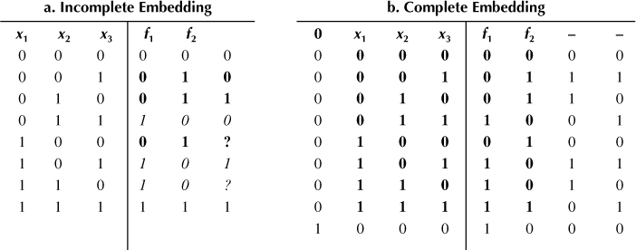
In case of the adder function, [log2(3)] = 2 additional outputs are required, because at most three output patterns are repeated, that is, μ = 3. Thus, besides the three primary inputs and two primary outputs, a reversible realization of an adder must consist of at least one constant input and two garbage outputs. A possible assignment to the newly added values is depicted in Table 11.3b (the original adder function is highlighted in bold).
For small functions to be synthesized (i.e., for functions given in terms of a truth table), keeping the number of circuit lines small is easily possible [19]. In fact, most of the respective approaches [20–22] generate circuits with a minimal number of circuit lines. However, for larger functions (i.e., for functions that cannot be represented in terms of a truth table any longer), keeping the number of circuit lines minimal is significantly harder. In fact, most of the existing approaches [23–25] often lead to circuits that are way beyond the optimum of the number of lines [26].
11.5.2 Synthesis
Synthesis is one of the most important steps while building complex circuits. Considering the conventional design flow, synthesis is carried out in several individual steps such as high-level synthesis, logic synthesis, mapping, and routing. To synthesize reversible logic, adjustments and extensions are needed. For example, throughout the whole flow, the restrictions caused by the reversibility (no fanout and feedback) and a completely new gate library must be considered.
Existing synthesis approaches addressing these issues can be categorized as follows:
Boolean synthesis approaches for small functions: These approaches can handle small Boolean functions, for example, provided in terms of permutations [20,27], truth tables [21,28,29], positive-polarity Reed-Muller expansion [22], or Reed-Muller spectra [30]. Besides, exact approaches exist that do not only generate a reversible circuit for a given function, but in addition ensure that the resulting circuit is composed of a minimal number of gates [31].
The scalability of all these approaches is thereby limited. Usually, only circuits for functions containing not more than 30 variables can be obtained with them. Hence, if larger functions should be synthesized, more compact function descriptions and, accordingly, other synthesis approaches have to be considered.
Boolean synthesis approaches for larger functions: Synthesis methods for larger functions make use of more compact function representations. In particular, approaches based on exclusive sum of products [23] and approaches based on binary decision diagrams [24] fall into this category. Here, the structure of the function representation is mapped to respective reversible subcircuits. By cascading the resulting subcircuits, the overall function is realized.
Synthesis approach based on a programming language: Although the previous approaches rely on Boolean descriptions for the synthesis of reversible circuits, recently a programming language has been proposed for this purpose [25]. This language, called SyReC, enables the design of more complex reversible systems.
11.5.3 Optimization
After synthesis, the resulting circuits often are of high cost. In particular, dedicated technology-specific constraints are not considered by synthesis approaches. To address this, optimization methods have been introduced. In particular, the reduction of the quantum cost of given circuits has been considered [28,32–34]. Also, reducing the number of circuit lines [35] or optimization of further, more technology-dependent cost metrics [36] was the subject of research activities.
11.5.4 Verification and Debugging
To ensure that the respective results (e.g., obtained by optimization) still represent the desired functionality, verification is applied. For this purpose, first verification approaches have been introduced [37–40]. Moreover, even automatic debugging methods aimed at supporting the designer to detect the error in case of a failed verification are already available [41].
11.6 Conclusions
In this chapter, the basics, promising applications, and the current state of the art of the design of reversible circuits have been briefly reviewed. Although circuits based on the conventional computation paradigm will reach fundamental limits in the future, reversible circuits find useful applications in emerging technologies such as quantum computing, and have benefits to be exploited in the domain of low-power design.
However, design of reversible circuits is just at the beginning. Considering the existing design methods, many of the proposed approaches have limitations with respect to the size of the function to be synthesized or the circuit to be considered. Furthermore, circuits obtained by current synthesis approaches often are of significant costs. Besides that, no integrated design flow for complex reversible circuits exists so far. Hence, further research in this promising area is required.
References
1. M. Nielsen and I. Chuang. Quantum Computation and Quantum Information. Cambridge University Press: NYC, 2000.
2. T. Toffoli. Reversible computing. In Automata, Languages and Programming, W. de Bakker and J. van Leeuwen (Eds.), p. 632. Technical Memo MIT/LCS/TM-151. Springer: Berlin, Heidelberg, 1980.
3. L. K. Grover. A fast quantum mechanical algorithm for database search. In Proceedings of Theory of Computing, pp. 212–219. Philadelphia, PA, 1996.
4. P. W. Shor. Algorithms for quantum computation: Discrete logarithms and factoring. In Proceedings of Foundations of Computer Science, pp. 124–134. Santa Fe, NM, 1994.
5. L. M. K. Vandersypen, M. Steffen, G. Breyta, C. S. Yannoni, M. H. Sherwood, and I. L. Chuang. Experimental realization of Shor’s quantum factoring algorithm using nuclear magnetic resonance. Nature, 414: 883–887, 2001.
6. A. Barenco, C. H. Bennett, R. Cleve, D. P. DiVinchenzo, N. Margolus, P. Shor, T. Sleator, J. A. Smolin, and H. Weinfurter. Elementary gates for quantum computation. The American Physical Society, 52: 3457–3467, 1995.
7. Z. Sasanian, R. Wille, D. M. Miller, and R. Drechsler. Realizing reversible circuits using a new class of quantum gates. In Design Automation Conference, pages 36–41. San Francisco, CA, 2012.
8. D. M. Miller, R. Wille, and Z. Sasanian. Elementary quantum gate realizations for multiple-control Toffoli gates. In International Symposium on Multi-Valued Logic, pp. 288–293. Tuusula, Finland, 2011.
9. M. Soeken, Z. Sasanian, R. Wille, D. M. Miller, and R. Drechsler. Optimizing the mapping of reversible circuits to four-valued quantum gate circuits. In International Symposium on Multi-Valued Logic, pp. 173–178. Victoria, BC, 2012.
10. R. Landauer. Irreversibility and heat generation in the computing process. IBM Journal of Research and Development, 5: 261–269, 1961.
11. P. Zeitzoff and J. Chung. A perspective from the 2003 ITRS. IEEE Circuits and Systems Magazine, 21: 4–15, 2005.
12. N. Gershenfeld. Signal entropy and the thermodynamics of computation. IBM Systems Journal, 35(3–4): 577–586, 1996.
13. C. H. Bennett. Logical reversibility of computation. IBM Journal of Research and Development, 17(6): 525–532, 1973.
14. A. Berut, A. Arakelyan, A. Petrosyan, S. Ciliberto, R. Dillenschneider, and E. Lutz. Experimental verification of Landauer’s principle linking information and thermodynamics. Nature, 483: 187–189, 2012.
15. S. Pasricha and N. Dutt. On-Chip Communication Architectures: Systems on Chip. Morgan Kaufman, Burlington, MA, 2008.
16. S. Ramprasad, N. R. Shanbhag, and I. N. Hajj. A coding framework for low-power address and data busses. IEEE Transactions on Very Large Scale Integration (VLSI) Systems, 7(2): 212–220, 1999.
17. L. Benini, A. Macii, E. Macii, M. Poncino, and R. Scarsi. Architectures and synthesis algorithms for power-efficient bus interfaces. IEEE Transactions on Computer-Aided Design of Integrated Circuits and Systems, 19: 969–980, 2000.
18. B. Desoete and A. De Vos. A reversible carry-look-ahead adder using control gates. Integration, the VLSI Journal, 33(1–2): 89–104, 2002.
19. D. Maslov and G. W. Dueck. Reversible cascades with minimal garbage. IEEE Transactions on Computer-Aided Design, 23(11): 1497–1509, 2004.
20. V. V. Shende, A. K. Prasad, I. L. Markov, and J. P. Hayes. Synthesis of reversible logic circuits. IEEE Transactions on Computer-Aided Design, 22(6): 710–722, 2003.
21. D. M. Miller, D. Maslov, and G. W. Dueck. A transformation based algorithm for reversible logic synthesis. In Design Automation Conference, pp. 318–323. Anaheim, CA, 2003.
22. P. Gupta, A. Agrawal, and N. K. Jha. An algorithm for synthesis of reversible logic circuits. IEEE Transactions on Computer-Aided Design, 25(11): 2317–2330, 2006.
23. K. Fazel, M. A. Thornton, and J. E. Rice. ESOP-based Toffoli gate cascade generation. In IEEE Pacific Rim Conference on Communications, Computers and Signal Processing (PacRim 2007), pp. 206–209. Victoria, BC, 2007.
24. R. Wille and R. Drechsler. BDD-based synthesis of reversible logic for large functions. In Design Automation Conference, pp. 270–275. San Francisco, CA, 2009.
25. R. Wille, S. Offermann, and R. Drechsler. SyReC: A programming language for synthesis of reversible circuits. In Forum on Specification and Design Languages, pp. 184–189. Southampton, UK, 2010.
26. R. Wille, O. Keszöcze, and R. Drechsler. Determining the minimal number of lines for large reversible circuits. In Design, Automation and Test in Europe, pp. 1204–1207. Grenoble, France, 2011.
27. M. Saeedi, M. S. Zamani, M. Sedighi, and Z. Sasanian. Synthesis of reversible circuit using cycle-based approach. ACM Journal of Emerging Technologies Computing Systems, 6(4), 2010.
28. D. Maslov, G. W. Dueck, and D. M. Miller. Toffoli network synthesis with templates. IEEE Transactions on Computer-Aided Design, 24(6): 807–817, 2005.
29. R. Wille, D. Grosse, G. W. Dueck, and R. Drechsler. Reversible logic synthesis with output permutation. In VLSI Design, pp. 189–194. New Delhi, India, 2009.
30. D. Maslov, G. W. Dueck, and D. M. Miller. Techniques for the synthesis of reversible Toffoli networks. ACM Transactions on Design Automation of Electronic Systems, 12(4), 2007.
31. D. Grosse, R. Wille, G. W. Dueck, and R. Drechsler. Exact multiple control Toffoli network synthesis with SAT techniques. IEEE Transactions on Computer-Aided Design, 28(5): 703–715, 2009.
32. K. Iwama, Y. Kambayashi, and S. Yamashita. Transformation rules for designing CNOT-based quantum circuits. In Design Automation Conference, pp. 419–424. New Orleans, LA, 2002.
33. J. Zhong and J. C. Muzio. Using crosspoint faults in simplifying Toffoli networks. In IEEE North-East Workshop on Circuits and Systems, pp. 129–132. Gatineau, Quebec, Canada, 2006.
34. D. M. Miller, R. Wille, and R. Drechsler. Reducing reversible circuit cost by adding lines. In International Symposium on Multi-Valued Logic, pp. 217–222. Barcelona, Spain, 2010.
35. R. Wille, M. Soeken, and R. Drechsler. Reducing the number of lines in reversible circuits. In Design Automation Conference, pp. 647–652. Anaheim, CA, 2010.
36. M. Saeedi, R. Wille, and R. Drechsler. Synthesis of quantum circuits for linear nearest neighbor architectures. Quantum Information Processing, 10(3): 355–377, 2011.
37. G. F. Viamontes, I. L. Markov, and J. P. Hayes. Checking equivalence of quantum circuits and states. In International Conference on Computer-Aided Design, pp. 69–74. San Jose, CA, 2007.
38. S. Gay, R. Nagarajan, and N. Papanikolaou. QMC: A model checker for quantum systems. In Computer Aided Verification, pp. 543–547. Springer, Berlin, Germany, 2008.
39. S.-A. Wang, C.-Y. Lu, I.-M. Tsai, and S.-Y. Kuo. An XQDD-based verification method for quantum circuits. IEICE Transactions, 91-A (2): 584–594, 2008.
40. R. Wille, D. Grosse, D. M. Miller, and R. Drechsler. Equivalence checking of reversible circuits. In International Symposium on Multi-Valued Logic, pp. 324–330. Naha, Okinawa, Japan, 2009.
41. R. Wille, D. Grosse, S. Frehse, G. W. Dueck, and R. Drechsler. Debugging of Toffoli networks. In Design, Automation and Test in Europe, pp. 1284–1289. Nice, France, 2009.