
14 Future of Asynchronous Logic
Scott C. Smith and Jia Di
Contents
14.2 Modern Asynchronous Logic
14.1 Introduction
The 2012 International Technology Roadmap for Semiconductors (ITRS) [1] states that asynchronous circuits currently account for 22% of logic within the multibillion dollar semiconductor industry, and predicts that this percentage will more than double over the next 10 years. Asynchronous logic has been around for the past 50+ years, but, until recently, synchronous circuits have been good enough to meet industry needs, so asynchronous circuits were primarily utilized for niche markets and in the research domain. However, as transistor size continues to decrease, asynchronous circuits are being looked to by industry to solve power dissipation and process variability issues associated with these emerging sub-90 nm circuits. This chapter details the state of the art of asynchronous logic, how asynchronous circuits are currently being utilized in the industry, and the future of asynchronous logic.
14.2 Modern Asynchronous Logic
Asynchronous circuits were originally designed using a bounded-delay model, which assumes that delays in both gates and wires are known, or at least bounded [2]. This requires delays to be added based on worst-case scenarios to avoid hazard conditions, which leads to extensive timing analysis to ensure correct circuit operation. In addition, bounded-delay asynchronous circuits are not suited to datapath design. Hence, micropipelines [3] were developed to avoid these issues by utilizing a bounded-delay datapath along with delay-insensitive control. Micropipelines utilize the bundled data convention, where the datapath consists of standard Boolean logic with an extra ready signal that matches the worse-case delay in the datapath to ensure that data is valid before being latched at the subsequent register. However, micropipelines still require timing analysis and delay matching, resulting in worse-case delay. Therefore, asynchronous logic research turned to completely delay-insensitive circuits, which assume that delays in both gates and wires are unbounded; however, this assumption severely limits circuit practicality [4]. So, isochronic wire forks [5,6] are assumed within basic components, such as a full-adder, meaning that wire delays within a component are assumed to be much less than the logic element delays within the component. Wires connecting components do not have to adhere to the isochronic fork assumption, making this a valid supposition even in current and future nanometer technologies. Delay-insensitive circuits with this isochronic fork assumption are referred to as quasi-delay-insensitive (QDI), and are the basis for most modern day asynchronous circuits. QDI circuits operate in the presence of indefinite arrival times for the reception of inputs, and utilize completion detection of output signals to provide handshaking control of input wave fronts. QDI circuits therefore require very little, if any, timing analysis to ensure correct operation (i.e., they are correct-by-construction), and also yield average-case performance rather than the worse-case performance of bounded-delay and synchronous paradigms.
Figure 14.1 shows a generalized block diagram of a QDI system, where QDI combinational logic is sandwiched between QDI registers, which is very similar to synchronous circuits, with the difference being that synchronous circuits utilize a clock signal to simultaneously latch data at the registers, whereas QDI circuits utilize completion detection of the combinational logic signals to generate handshaking signals that are used to latch data at a register. Note that some QDI paradigms combine combinational logic and registration together into single components, and the method of generating handshaking signals also varies.
Synchronous, bounded-delay asynchronous, and micropipelines all use a single wire to encode one bit of data: GND is encoded as Logic 0 and VDD is encoded as Logic 1; the outputs of a computation are then sampled after waiting a predetermined amount of time that is long enough to ensure that the computation has been completed. On the other hand, QDI circuits do not rely on timing to determine when a computation has finished, so they require a different way of encoding data to determine computation completion. Typically, a 1-hot encoding scheme is utilized, such as dual-rail logic, depicted in Table 14.1, where two wires, D0 and D1, are used to encode one bit of data. D0 being asserted is referred to as DATA0 and depicts a Logic 0; D1 being asserted is referred to as DATA1 and depicts a Logic 1; and neither D0 nor D1 being asserted is referred to as the spacer, or NULL, state, which depicts that the computation has not yet finished. Note that D0 and D1 are mutually exclusive, such that both rails can never be asserted simultaneously; this state is illegal, and will never occur in a properly operating system.
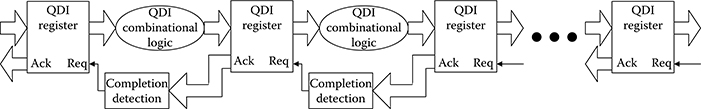
FIGURE 14.1 Quasi-delay-insensitive system framework: input wave fronts are controlled by local handshaking signals and completion detection instead of by a global clock signal. Feedback requires at least three quasi-delay-insensitive registers in the feedback loop to prevent deadlock.
Table 14.1 Dual-Rail Signal
|
DATA0 |
DATA1 |
NULL |
Illegal |
D0 |
1 |
0 |
0 |
1 |
D1 |
0 |
1 |
0 |
1 |
Using dual-rail logic, timing is no longer needed to determine computation completion. Starting with the system in an all NULL state, DATA is input to the system, which flows through the combinational logic, eventually transitioning all of the outputs to DATA, which depicts that the computation has finished. The system must then transition back into the all NULL state before the next DATA wave front is input to the system. NORing the two rails of a dual-rail signal generates a Logic 0 when DATA and a Logic 1 when NULL, which can be used as an acknowledge signal. To signal when all outputs are DATA or NULL, to determine when the computation or return to NULL has finished, respectively, the acknowledge signals must all be combined together using what is referred to as a C-element [7]. A C-element only changes state when all inputs are the same; when all inputs are asserted, the output is asserted, which then remains asserted until all inputs are deasserted, which requires internal feedback within the C-element gate. The C-element output can then be used to request the next DATA wave front input when asserted, and the return to NULL when deasserted.
Of the various implementations of QDI circuits, there are two main paradigms that have been primarily utilized in industry: NULL convention logic (NCL) [8] and precharge half buffers (PCHB) [9].
14.2.1 Null Convention Logic
NCL circuits are composed of 27 fundamental gates, as shown in Table 14.2, which constitute the set of all functions consisting of four or fewer variables. Because each rail of an NCL signal is considered a separate variable, a four-variable function is not the same as a function of four literals, which would consist of eight variables for dual-rail logic (e.g., a literal includes both a variable and its complement, F and F’, whereas NCL rails are never complemented, such that a dual-rail NCL signal, F, consists of two variables, F1 and F0, where F0 is equivalent to F′). The primary type of threshold gate, shown in Figure 14.2a, is the THmn gate, where 1 ≤ m ≤ n. THmn gates have n inputs, and at least m of the n inputs must be asserted before the output will become asserted. In a THmn gate, each of the n inputs is connected to the rounded portion of the gate; the output emanates from the pointed end of the gate; and the gate’s threshold value, m, is written inside of the gate.
Another type of threshold gate is referred to as a weighted threshold gate, denoted as THmnWw1w2…wR. Weighted threshold gates have an integer value, m ≥ wR > 1, applied to inputR. Here 1 ≤ R < n; where n is the number of inputs; m is the gate’s threshold; and w1, w2, … wR, each > 1, are the integer weights of input1, input2, … inputR, respectively. For example, consider the TH34w2 gate, whose n = 4 inputs are labeled A, B, C, and D, shown in Figure 14.2b. The weight of input A is therefore 2. Because the gate’s threshold, m, is 3, this implies that in order for the output to be asserted, either inputs B, C, and D must all be asserted, or input A must be asserted along with any other input, B, C, or D.
Table 14.2 Twenty-Seven Fundamental NULL Convention Logic Gates
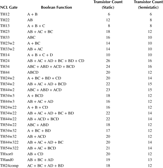
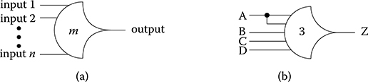
FIGURE 14.2 NULL convention logic threshold gates: (a) THmn Gate; (b) TH34w2 Gate: Z = AB + AC + AD + BCD.
NCL threshold gates are designed with hysteresis state-holding capability, such that after the output is asserted, all inputs must be deasserted before the output will be deasserted. Hysteresis ensures a complete transition of inputs back to NULL before asserting the output associated with the next wave front of input data. Hence, a THnn gate is equivalent to an n-input C-element, and a TH1n gate is equivalent to an n-input OR gate. NCL threshold gates may also include a reset input to initialize the output. Circuit diagrams designate resettable gates by either a d or an n appearing inside the gate, along with the gate’s threshold. d denotes the gate as being reset to Logic 1; n, to Logic 0. These resettable gates are used in the design of NCL registers.
NCL systems contain at least two NCL registers, one at both the input and at the output. Two adjacent register stages interact through their request and acknowledge signals, Ki and Ko, respectively, to prevent the current DATA wave front from overwriting the previous DATA wave front, by ensuring that the two DATA wave fronts are always separated by a NULL wave front. The acknowledge signals are combined in the completion detection circuitry to produce the request signal(s) to the previous register stage, as depicted in Figure 14.1. NCL registration is realized through cascaded arrangements of single-bit dual-rail registers, depicted in Figure 14.3. A dual-rail register consists of two TH22 gates (2-input C-elements) that pass a DATA value at the input only when Ki is request for data (rfd) (i.e., Logic 1), and likewise pass NULL only when Ki is request for null (rfn) (i.e., Logic 0). They also contain a NOR gate to generate Ko, which is rfn when the register output is DATA and rfd when the register output is NULL. The register depicted in Figure 14.3 is reset to NULL, because both TH22 gates are reset to Logic 0. However, the register could be instead reset to DATA0 or DATA1 by replacing exactly one of the TH22n gates with a TH22d gate.
An N-bit register stage, composed of N single-bit dual-rail NCL registers, requires N completion signals, one for each bit. The NCL completion component, shown in Figure 14.4, uses these N Ko lines to detect complete DATA and NULL sets at the output of every register stage and request the next NULL and DATA set, respectively. In full-word completion, the single-bit output of the completion component is connected to all Ki lines of the previous register stage. Because the maximum input threshold gate is the TH44 gate, the number of logic levels in the completion component for an N-bit register is given by |log4 N|. Figures 14.5 and 14.6 show the flow of DATA and NULL wave fronts through an NCL combinational circuit (i.e., an AND function) and an arbitrary pipeline stage, respectively. The average DATA/NULL cycle time, referred to as TDD, is comparable to the clock frequency of a synchronous circuit.
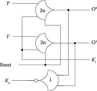
FIGURE 14.3 Single-bit dual-rail register.
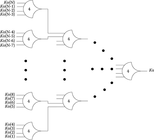
FIGURE 14.4 N-bit completion component.
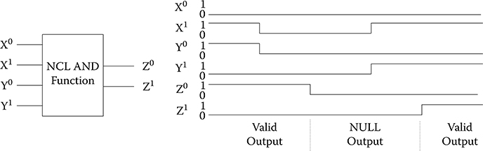
FIGURE 14.5 NULL convention logic AND function: Z = X · Y: initially X = DATA1 and Y = DATA0, so Z = DATA0; next X and Y both transition to NULL, so Z transitions to NULL; then X and Y both transition to DATA1, so Z transitions to DATA1.
Because NCL threshold gates are designed with hysteresis state-holding capability, which requires internal feedback, NCL gates require both set and hold equations, where the set equation determines when the gate will become asserted and the hold equation determines when the gate will remain asserted once it has been asserted. The set equation determines the gate’s functionality as one of the 27 NCL gates, as listed in Table 14.2, whereas the hold1 equation is simply all inputs ORed together, to ensure that the output remains asserted until all inputs are deasserted. The general equation for an NCL gate with output Z is Z = set + (Z− · hold1), where Z− is the previous output value and Z is the new value.
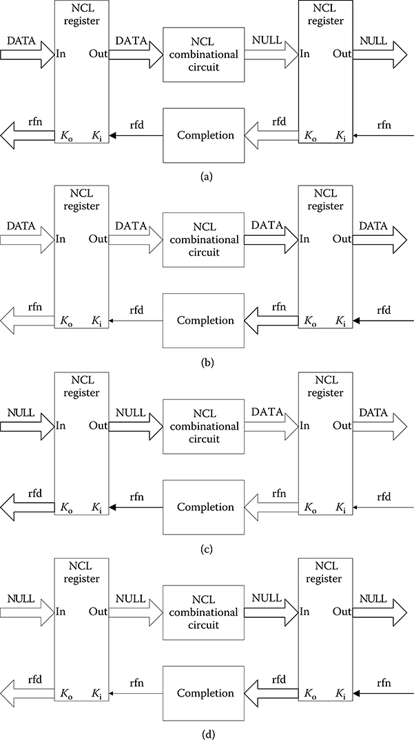
FIGURE 14.6 NULL convention logic DATA/NULL cycle. (a) DATA flowing through input register then combinational logic. (b) DATA flowing through output register then rfn flowing through completion logic. (c) NULL flowing through input register then combinational logic. (d) NULL flowing through output register then rfd flowing through completion logic.
To implement an NCL gate using complementary metal–oxide–semiconductor (CMOS) technology, an equation for the complement of Z is also required, which in general form is: Z′ = reset + (Z−′ · hold0), where reset is the complement of hold1 (i.e., the complement of each input, ANDed together) and hold0 is the complement of set, such that the gate output is deasserted when all inputs are deasserted, and then remains deasserted while the gate’s set condition is false. As shown in Figure 14.7, for the static realization, the equations for Z and Z′, given in this paragraph and the preceding paragraph, respectively, are directly implemented in the NMOS and PMOS logic, respectively, after simplifying, whereas, the semistatic realization only requires the set and reset equations to be implemented in the NMOS and PMOS logic, respectively, and hold0 and hold1 are implemented using a weak feedback inverter.
For example, the set equation for the TH23 gate is AB + AC + BC, as given in Table 14.2, and the hold equation is A + B + C; therefore, the gate is asserted when at least two inputs are asserted, and then remains asserted until all inputs are deasserted. The reset equation is A′B′C′ and the simplified set′ equation is A′B′ + B′C′ + A′C′. Directly implementing these equations for Z and Z′, after simplification, yields the static transistor-level realization shown in Figure 14.8a. The semistatic TH23 gate is shown in Figure 14.8b. In general, the semistatic implementation requires fewer transistors, but is slightly slower because of the weak inverter. Note that TH1n gates are simply OR gates and do not require any feedback, such that their static and semistatic implementations are exactly the same.
NCL combinational logic is designed utilizing the 27 NCL gates in Table 14.2, to generate a circuit that must be input-complete and observable [10], meaning that all outputs cannot transition from NULL to DATA until all inputs have transitioned from NULL to DATA, and that all asserted gates contribute to asserting at least one circuit output, respectively. Note that, for circuits with multiple outputs, it is acceptable according to Seitz’s “weak conditions” of delay-insensitive signaling [11], for some of the outputs to transition without having a complete input set present, as long as all outputs cannot transition before all inputs arrive. Figure 14.9 shows an example of an NCL full adder, and complete details of the methodology for designing NCL circuits can be found in Smith et al. [10].
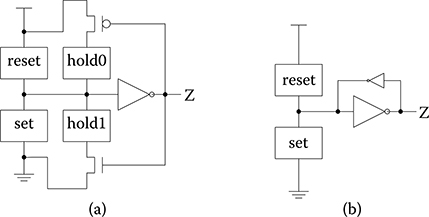
FIGURE 14.7 NULL convention logic gate realizations: (a) static implementation; (b) semi-static implementation.
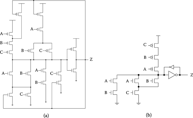
FIGURE 14.8 TH23 gate realizations: (a) static implementation; (b) semistatic implementation.
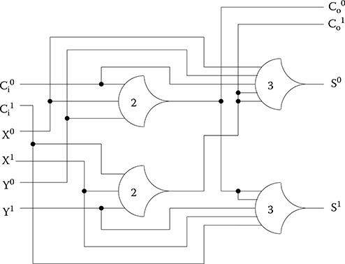
FIGURE 14.9 Optimized NULL convention logic full adder.
14.2.2 Precharge Half Buffers
PCHB circuits are designed at the transistor level, utilizing a style similar to domino logic, instead of targeting a predefined set of gates like NCL. PCHB circuits have dual-rail data inputs and outputs, and combine combinational logic and registration together into a single block, yielding a very fine-grain pipelined architecture.
Figure 14.10 shows an example of a PCHB NAND2 circuit. The dual-rail output is initially precharged to NULL. When request (Rack) and acknowledge (Lack) are both rfd, the specific function will evaluate when the inputs, X and/or Y, become DATA, causing the output, F, to become DATA. Lack will then transition to rfn only after all inputs and the output are DATA. When Rack is rfn and Lack is rfd, or vice versa, the output will be floating, so weak inverters must be used to hold the current output value to maintain delay-insensitivity. After both Rack and Lack are rfn, the output will be precharged back to NULL. After all inputs become NULL and the output changes to NULL, Lack will change back to rfd, and the next DATA wave front can evaluate after Rack becomes rfd. Note that Rack and Lack are equivalent to NCL’s Ki and Ko, respectively, and both PCHB and NCL utilize the same protocol, referred to as four-phase return-to-zero handshaking.
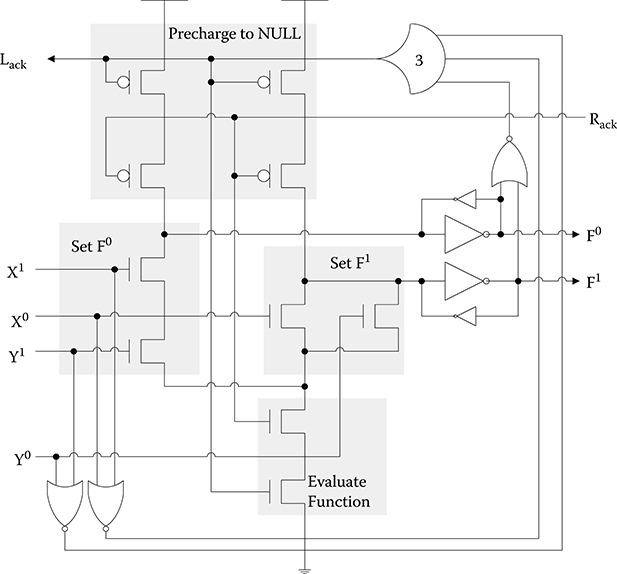
FIGURE 14.10 Precharge half buffer NAND2 circuit.
Different from NCL, in PCHB, computation and registration are integrated into a single transistor-level component, which ensures observability; and both the inputs and outputs of a component are used to generate acknowledge signals, which ensures input completeness.
14.3 Asynchronous Circuits in Industry
There have been a number of start-up companies developing asynchronous logic technology and products over the past 15 years, including Handshake Solutions, Tiempo, Theseus Logic, NanoWatt Design, Fulcrum Microsystems, and Achronix Semiconductor Corporation. Handshake Solutions was a line of business of Philips Electronics’ Technology Incubator that most notably developed low-power micro-pipeline-based bundled data asynchronous 8051 microcontrollers and ARM processors for the smart card and automotive markets; however, Handshake Solutions no longer exists. Tiempo is a fabless IC company that licenses asynchronous IP cores and accompanying automated design tools, based on their proprietary technology, which like NCL and PCHB, utilizes dual-rail logic and four-phase return-to-zero handshaking [12]. Theseus Logic, founded by the inventor of NCL, partnered with a number of companies, such as Motorola and Atmel, to develop an asynchronous microprocessor core, field-programmable gate array (FPGA), and automated design tools. Theseus Logic no longer exists; however, their NCL technology is currently being used by Camgian Microsystems to design low-power highly integrated mixed-signal Systems-on-Chip (SoCs) for wireless sensor nodes [13], and variations of NCL are being utilized by NanoWatt Design, a fabless IC company focusing on ultra-low power asynchronous design for use in mobile electronics and other devices requiring low power, such as wireless sensor nodes, utilizing their proprietary sleep convention logic (SCL) technology [14], and by Wave Semiconductor to develop a proprietary low-power, high-speed, low-cost reprogrammable device, called Azure, which is structured as a 2D mesh of byte-level processing elements that can be quickly and partially reconfigured to support expedient hardware context switching [15].
SCL, also referred to as MTNCL, combines NCL with multithreshold CMOS [16], to yield a patented and patent-pending ultra-low power asynchronous circuit design methodology [17–19]. SCL utilizes the same dual-rail logic and four-phase return-to-zero handshaking as other QDI paradigms; however, instead of propagating the NULL wave front to reset all gates to zero as in NCL, all gates in a stage are simultaneously slept to zero using the handshaking signals. This requires a modification in the overall architecture, shown in Figure 14.11, and in the gate design. The completion logic inputs now come from the register inputs, instead of register outputs, and require the completion signal from the previous stage as an additional input, which is referred to as Early Completion [20]. The new gate design, used to implement the combinational logic and completion logic, now includes a sleep input, and no longer requires internal hysteresis feedback, as shown in Figure 14.12. This allows for SCL combinational logic to no longer require input-completeness and observability, because all logic in a stage is now simultaneously reset to NULL instead of propagating the NULL wave front, which results in substantially smaller and faster circuits. Also note that select high-threshold (high-Vt) transistors (shown in dotted circles in Figure 14.12) are utilized in SCL gates to ensure that all paths from VDD to GND include at least one high-Vt transistor that is off when the gate is deasserted, while using faster low-Vt transistors for the switching logic, to yield extremely low leakage power while the circuit is idle in the slept NULL state without substantially degrading speed.
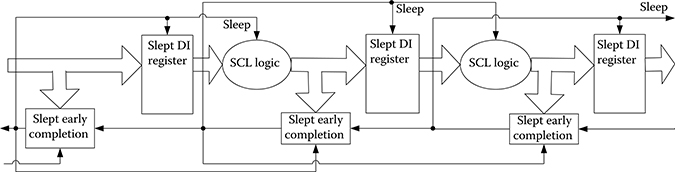
FIGURE 14.11 Sleep convention logic circuit architecture.
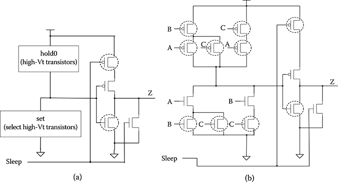
FIGURE 14.12 Sleep convention logic gate realization: (a) general implementation; (b) TH23 example.
Wave Semiconductor’s patent-pending technology is similar to SCL in that it can simultaneously sleep a stage’s gates to zero instead of propagating the NULL wave front, and can utilize select high-Vt transistors to reduce leakage power [21–23]. It utilizes a precharge transistor to pull up the internal node, causing the output to become zero, similar to PCHB. Like SCL, it utilizes a modified threshold gate design to build dual-rail combinational logic, combined with four-phase return-to-zero handshaking.
Fulcrum Microsystems utilized PCHB technology on a low-leakage 130-nm process to develop 4-port and then 24-port network switch chips, both of whose channels operated at 10 Gb speed with 200 ns latency through the chip, which were the fastest networking chips on the market. In 2011, Intel purchased Fulcrum Microsystems, who are now Intel Switch & Router Division, producing Ethernet switch chips with up to 64 10 Gb ports [24].
Achronix develops high-speed and low-power FPGAs that have a synchronous interface with an asynchronous core that utilizes PCHB technology [25]. Achronix FPGAs utilize Intel’s 22-nm 3D tri-gate FinFET process, and include high-density versions that offer up to 1.7 million effective LUTs that utilize approximately half the power of standard commercial synchronous FPGAs, and high-speed versions that offer up to 590 thousand effective LUTs and operate at up to 1.5 GHz, three to four times faster than commercial synchronous FPGAs. Achronix FPGAs are programmed using the Achronix CAD Environment (ACE), which works in conjunction with industry-standard tools to synthesize standard Very High Speed Integrated Circuit Hardware Description Language or Verilog RTL code.
14.4 The Next 10 Years
Ten years ago, in 2003, ITRS predicted a gradual industry shift from synchronous to asynchronous design styles to help mitigate power, robustness to process variation, and timing issues, as process technology continued to shrink [26]. The 2005 ITRS edition predicted asynchronous circuits to constitute 20% of the industry by 2012 [27]; this prediction was indeed confirmed in the latest 2012 ITRS update, which shows that asynchronous technology did account for 20% of the industry in 2012 [1]. Looking forward, ITRS predicts asynchronous circuits to account for 49% of the multibillion dollar semiconductor industry by 2024, and continue to grow to become the predominant design style [1]; hence, the future of asynchronous circuits is looking very bright.
QDI paradigms are the path forward for asynchronous circuits in the industry, because they do not rely on timing assumptions, which, due to process variation, are becoming more and more unpredictable as transistor size continues to shrink. QDI circuits are the underlying technology of all the major asynchronous companies mentioned in Section 14.3 whom are still in business, and are being utilized by the industry’s leader, Intel, who purchased Fulcrum Microsystems and is currently partnering with Achronix.
Looking back, the major impediments to asynchronous design becoming more prevalent in the industry were the lack of industry-standard CAD tools for asynchronous logic and comparatively little asynchronous expertise. Because synchronous circuits were good enough to produce next generation products, asynchronous solutions received little attention. However, as synchronous circuits are becoming more and more problematic for cutting-edge process technologies, QDI paradigms are being used much more frequently, and not just by start-up companies for niche markets, but also by industry leaders, like Intel. This transition has been aided by development of mature CAD tools for asynchronous logic, such as Achronix’s ACE, which hide the details of asynchronous circuits from designers, allowing them to utilize the current synchronous design style in which they are accustomed. Synchronous circuits will never go away entirely, because they are very good at performing certain tasks, such as measuring time (e.g., timers in a microcontroller). However, as asynchronous technology continues to increase its market share, comprising approximately one half of the multibillion dollar semiconductor industry within the next 10 years, circuit designers will be expected to know how to design asynchronous circuits as well as synchronous circuits; so, if you are new to asynchronous circuit design, the following references will help get you up to speed [9,10].
References
1. ITRS, ITRS 2012 update, available at http://www.itrs.net/Links/2012ITRS/Home2012.htm; accessed on October 2013.
2. S. H. Unger, Asynchronous Sequential Switching Circuits, Wiley, New York, NY, 1969.
3. E. Sutherland, “Micropipelines,” Communications of the ACM, 32(6): 720–738, 1989.
4. A. J. Martin, “The limitations to delay-insensitivity in asynchronous circuits,” MIT Conference on Advanced Research in VLSI, Cambridge, MA, pp. 263–278, 1990.
5. A. J. Martin, “Programming in VLSI,” in Development in Concurrency and Communication, Addison-Wesley, Reading, MA, pp. 1–64, 1990.
6. K. Van Berkel, “Beware the Isochronic Fork,” Integration, the VLSI Journal, 13(2): 103–128, 1992.
7. D. E. Muller, “Asynchronous logics and application to information processing,” in Switching Theory in Space Technology, pp. 289–297, Stanford University Press, Palo Alto, CA, 1963.
8. K. M. Fant and S. A. Brandt, “NULL Convention Logic: A complete and consistent logic for asynchronous digital circuit synthesis,” International Conference on Application Specific Systems, Architectures, and Processors, pp. 261–273, Chicago, IL, 1996.
9. A. J. Martin and M. Nystrom, “Asynchronous techniques for system-on-chip design,” Proceedings of the IEEE, 94(6), 1089–1120, 2006.
10. S. C. Smith and J. Di, “Designing asynchronous circuits using NULL convention logic (NCL),” Synthesis Lectures on Digital Circuits and Systems, Morgan & Claypool Publishers, San Rafael, CA, 4(1), July 2009.
11. C. L. Seitz, “System timing,” in Introduction to VLSI Systems, Addison-Wesley, pp. 218–262, Reading, MA, 1980.
12. Tiempo company website, available at http://www.tiempo-ic.com/, accessed on October 2013.
13. Camgian Microelectronics company website, available at http://www.camgian.com/, accessed on October 2013.
14. NanoWatt Design company website, available at http://www.nanowattdesign.com/, accessed on October 2013.
15. Wave Semiconductor company website, available at http://wavesemi.com/, accessed on October 2013.
16. S. Mutoh, T. Douseki, Y. Matsuya, T. Aoki, S. Shigematsu, and J. Yamada, “1-V power supply high-speed digital circuit technology with multithreshold-voltage CMOS,” IEEE Journal of Solid-State Circuits, 30(8): 847–854, August 1995.
17. Jia Di and Scott Christopher Smith, “Ultra-low power multi-threshold asynchronous circuit design,” U.S. Patent 7,977,972 B2, filed April 30, 2010, and issued July 12, 2011.
18. Jia Di and Scott Christopher Smith, “Ultra-low power multi-threshold asynchronous circuit design,” U.S. Patent 8,207,758 B2, filed July 1, 2011, and issued June 26, 2012.
19. Scott Christopher Smith and Jia Di, “Multi-threshold sleep convention logic without NSleep,” U.S. Patent Application 20130181740, filed July 18, 2013.
20. S. C. Smith, “Speedup of self-timed digital systems using early completion,” IEEE Computer Society Annual Symposium on VLSI, pp. 107–113, Pittsburgh, PA, 2002.
21. Wave Semiconductor, Inc., “Multi-Threshold Flash NCL Circuitry,” U.S. Patent Application 20130214813, filed August 22, 2013.
22. Wave Semiconductor, Inc., “Self-Ready Flash NULL Convention Logic,” U.S. Patent Application 20130214814, filed August 22, 2013.
23. Wave Semiconductor, Inc., “Implementation Method for Fast NCL Data Path,” U.S. Patent Application 20130249594, filed September 26, 2013.
24. Fulcrum Microsystem company website, available at http://www.fulcrummicro.com/, accessed on October 2013.
25. Achronix Semiconductor Corporation company website, available at http://www.achronix.com/, accessed on October 2013.
26. ITRS, International technology roadmap for semiconductors 2003 edition, Design, available at http://www.itrs.net/Links/2003ITRS/Design2003.pdf, accessed on October 2013.
27. ITRS. International technology roadmap for semiconductors 2005 edition, Design, available at http://www.itrs.net/Links/2005ITRS/Design2005.pdf, accessed on October 2013.