
19 Heterogeneous Memory Design
Chengen Yang, Zihan Xu, Chaitali Chakrabarti and Yu Cao
Contents
19.2 Nonvolatile Memory Background
19.2.2 Spin Torque Transfer Magnetic Random-Access Memory
19.2.3 Comparison of Energy and Latency in Scaled Technologies
19.3 Heterogeneous Memory Design
19.3.1 Case Study of Heterogeneous Memory
19.3.2.1 Heterogeneous Cache Architecture
19.3.2.2 Heterogeneous Architecture for Main Memory
19.4 Reliability of Nonvolatile Memory
19.4.1 Reliability of Phase-Change Memory
19.4.1.1 Enhancing Reliability of Phase-Change Memory
19.4.2 Reliability of Spin-Transfer Torque Magnetic Memory
19.4.2.1 Enhancing Reliability of Spin-Transfer Torque Magnetic Memory
19.1 Introduction
Memory systems are essential to all computing platforms. To achieve optimal performance, contemporary memory architectures are hierarchically constructed with different types of memories. On-chip caches are usually built with static random-access memory (SRAM), because of their high speed; main memory uses dynamic random-access memory (DRAM); large-scale external memories leverage nonvolatile devices, such as the magnetic hard disk or solid state disk. By appropriately integrating these different technologies into the hierarchy, memory systems have traditionally tried to achieve high access speed, low energy consumption, high bit density, and reliable data storage.
Current memory systems are tremendously challenged by technology scaling and are no longer able to achieve these performance metrics. With the minimum feature size approaching 10 nm, silicon-based memory devices, such as SRAM, DRAM, and Flash, suffer from increasingly higher leakage, larger process variations, and severe reliability issues. Indeed, these silicon-based technologies hardly meet the requirements of future low-power portable electronics or tera-scale high-performance computing systems. In this context, the introduction of new devices into current memory systems is a must.
Recently, several emerging memory technologies have been actively researched as alternatives in the post–silicon era. These include phase-change memory (PRAM), spin-transfer torque magnetic memory (STT-MRAM), resistive memory (RRAM), and ferroelectric memory (FeRAM). These devices are diverse in their physical operation and performance.
Figure 19.1 compares the device operation and performance of different types of memories [1]. As the figure illustrates, these nonvolatile memories (NVMs) have much lower static power consumption and higher cell density, as compared to SRAM or DRAM. But there is no winner of all: some of them have higher latency (e.g., PRAM and MRAM), and some have higher programming energy (e.g., PRAM). Moreover, akin to the scaled CMOS memory devices, one of the biggest design challenges is how to compensate for the excessive amount of variations and defects in the design of a reliable system.
This chapter introduces a top–down methodology for heterogeneous memory systems that integrate emerging NVMs with other type of memories. While PRAM and STT-MRAM are used as examples, for their technology maturity and scalability, the integration methodology is general enough for all types of memory devices. We first develop device-level compact models of PRAM and STT-MRAM based on physical mechanism and operations. The models cover material properties, process and environmental variations, as well as soft and hard errors. They are scalable with device dimensions, providing statistical yield prediction for robust memory integration. By embedding these device-level models into circuit- and architecture-level simulators, such a CACTI and GEM5, we evaluate a wide range of heterogeneous memory configurations, under various system constraints. We also provide a survey of existing heterogeneous memory architecture that shows superior timing or energy performance. Finally, to address the reliability issues of the emerging memory technologies such as multilevel cell (MLC) PRAM and STT-MRAM, we also show how to extract error models from device-level models and review existing techniques for enhancing their reliability.
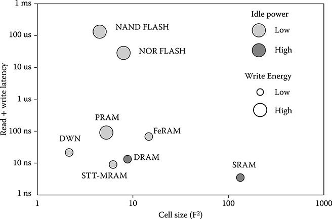
FIGURE 19.1 Diversity in memory operation and performance. (R. Venkatesan et al., “TapeCache: A high density, energy efficient cache based on domain wall memory,” ACM/IEEE International Symposium on Low Power Electronics and Design, ISLPED’12, © 2012 IEEE.)
This chapter is organized as follows: Section 19.2 gives a brief introduction to PRAM and STT-MRAM devices and derives the models. The device models are embedded into CACTI, SimpleScalar, and GEM5 to analyze heterogeneous memory architectures (Section 19.3). In Section 19.4, process variability and reliability effects are studied, followed by error characterization and compensation techniques. Section 19.5 concludes the chapter.
19.2 Nonvolatile Memory Background
19.2.1 Phase Change Memory
The structure of a PRAM cell is shown in Figure 19.2a. It consists of a standard NMOS transistor and a phase change device. The phase change device is built with a chalcogenide-based material, usually Ge2Sb2Te5 (GST), that is put between the top electrode and a metal heater that is connected to the bottom electrode. GST switches between a crystalline phase (low resistance) and an amorphous phase (high resistance) with the application of heat; the default phase of this material is crystalline. The region under transition is referred to as programmable region. The shape of the programmable region is usually of mushroom shape due to the current crowding effect at the heater to phase change material contact [2].
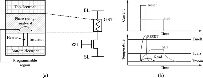
FIGURE 19.2 (a) Phase-change memory cell structure (H. S. P. Wong et al., “Phase change memory,” Proceedings of the IEEE, pp. 2201–2227, © 2010 IEEE.) (b) Phase-change memory cells are programmed and read by applying electrical pulses with different characteristics.
During write operation of single-level cell (SLC) PRAM, a voltage is applied to the word line (WL), and the current driver transistor generates the current that passes between the top and bottom electrodes to heat the heater, causing a change in the phase of the GST material. During write-0 or RESET operation, a large current is applied between top and bottom electrodes (see Figure 19.3b). This heats the programmable region over its melting point, which when followed by a rapid quench, turns this region into an amorphous phase. During write-1 or SET operation, a lower current pulse is applied for a longer period of time (see Figure 19.3b) so that the programmable region is at a temperature that is slightly higher than the crystallization transition temperature. A crystalline volume with radius r′ starts growing at the bottom of the programmable region as shown in Figure 19.3b. At the end of this process, the entire programmable region is converted back to the crystalline phase. In read operation, a low voltage is applied between the top and bottom electrodes to sense the device resistance. The read voltage is set to be sufficiently high to provide a current that can be sensed by a sense amplifier but low enough to avoid write disturbance [2].
Because the resistance between the amorphous and crystalline phases can exceed two to three orders of magnitude [3], multiple logical states corresponding to different resistance values can be accommodated. For instance, if four states can be accommodated, the PRAM cell is a 2-bit MLC PRAM. The four states of such a cell are “00” for full amorphous state, “11” for full crystalline state, and “01” and “10” for two intermediate states. MLC PRAM can be programmed by shaping the input current profile [2]. To go to “11” state from any other state, a SET pulse of low amplitude and long width is applied. However, to go to “00” state from any other state, it has to first transition to “11” state to avoid over programming. To go to “01” or “10” state, it first goes to “00” state and then to the final state after application of several short pulses. After each pulse, the read and verify method is applied to check whether the correct resistance value has been reached.
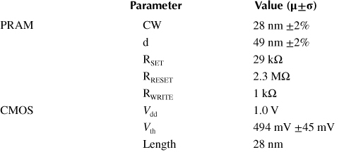
PRAM cell resistance is determined by the programming strategy and current profile. The Simulation Program with Integrated Circuit Emphasis (SPICE) parameters needed to simulate a PRAM cell are given in Table 19.1. These are used to obtain the initial resistance distributions of the four logical states of a 2-bit MLC PRAM. The variation in these parameters is used to calculate the shifts in these distributions, which again affect the error rate.
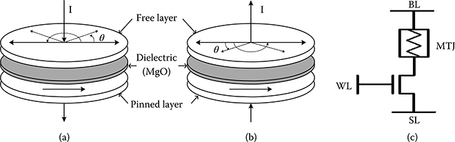
FIGURE 19.3 Spin-transfer torque magnetic memory structure: (a) parallel, (b) antiparallel, and (c) magnetic tunneling junction circuit structure.
Table 19.1 Phase-Change Memory Cell Parameter Values Used in SPICE Simulation for 45-nm Technology Node
The parameter values in Table 19.1 are used to calculate the energy and latency of read and write operations of a single cell PRAM. These values are then embedded into CACTI [4] to generate the energy and latency of a PRAM bank, as will be described in Section 19.3. Our approach is similar to that in Dong et al. (2009) and Dong et al. (2012) [5,6] where SLC PRAM parameters are embedded into CACTI to enable system-level study of energy consumption and latency [7,8].
19.2.2 Spin Torque Transfer Magnetic Random-Access Memory
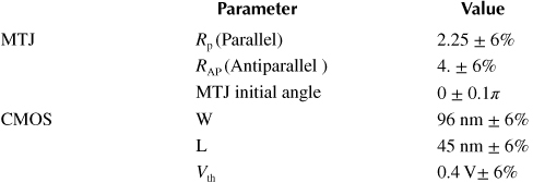
In STT-MRAM, the resistance of the magnetic tunneling junction (MTJ) determines the logical value of the data that is stored. MTJ consists of a thin layer of insulator (spacer-MgO) about ~1 nm thick sandwiched between two layers of ferromagnetic material [9]. Magnetic orientation of one layer is kept fixed and an external field is applied to change the orientation of the other layer. Direction of magnetization angle (parallel [P] or antiparallel [AP]) determines the resistance of MTJ, which is translated into storage value. Low resistance (parallel) state that is accomplished when magnetic orientation of both layers is in the same direction corresponds to storage of bit 0. By applying external field higher than critical field, magnetization angle of free layer is flipped by 180°, which leads to a high resistance state (antiparallel). This state corresponds to storage of bit 1. The difference between the resistance values of parallel and antiparallel states is called tunneling magnetoresistance (TMR) defined as TMR = (RAP − RP) / RP, where RAP and RP are the resistance values at antiparallel and parallel states, respectively. Increasing the TMR ratio makes the separation between states wider and improves the reliability of the cell [10]. Figure 19.3a and b highlights the parallel and antiparallel states.
Figure 19.3c describes the cell structure of an STT-MRAM cell. It consists of an access transistor in series with the MTJ resistance. The access transistor is controlled through WL, and the voltage levels used in bit lines (BLs) and select lines (SLs) determine the current that is used to adjust the magnetic field. There are three modes of operation, read, write-0, and write-1.
For read operation, current (magnetic field) lower than critical current (magnetic field) is applied to MTJ to determine its resistance state. Low voltage (~0.1 V) is applied to BL, and SL is set to ground. When the access transistor is turned on, a small current passes through MTJ whose value is detected based on a conventional voltage sensing or self-referencing schemes [11].
During write operation, BL and SL are charged to opposite values depending on the bit value that is to be stored. During write-0, BL is high and SL is set to zero, whereas during write-1, BL is set to zero and SL is set to high. We distinguish between write-0 and write-1 because of the asymmetry in their operation. For instance, in 45-nm technology, write-1 needs 245 μA programming current while write-0 requires 200 μA.
A physical model of MTJ based on the energy interaction is presented [12]. Energies acting in MTJ are Zeeman, anisotropic, and damping energy [13] and the state change of an MTJ cell can be derived by combining these energy types:
Here is the magnetic moment, Ms is the saturation magnetization, µ0 is the vacuum permeability, α is the damping constant, H is the magnetic field, θ is the magnetic angle of the free dielectric, and K is the anisotropic constant. Such an equation can be modeled using Verilog-A to simulate the circuit characteristics of STT-MRAM [12]. For instance, differential terms are modeled using capacitance, whereas Zeeman and damping energy are described by voltage-dependent current source.
The nominal values and variance of the device parameters are listed in Table 19.2. We consider 40 mV variation for random dopant fluctuation (RDF) when the width of 128 nm is equivalent to W/L = 4, and scaled it for different W/L ratios. The SPICE values have been used to calculate the energy and latency of a single cell during read and write operations and embedded into CACTI for system-level simulation. The parameter variations have been used to estimate the error rates as will be demonstrated in Section 19.4.
Table 19.2 Spin-Transfer Torque Magnetic Memory Parameter Values Used in SPICE Simulation for 45-nm Technology Node
19.2.3 Comparison of Energy and Latency in Scaled Technologies
The parameter values of NVM memories are embedded into CACTI [4] and used to generate the latency and energy results presented in this section. Because PRAM and STT-MRAM are resistive memories, the equations for BL energy and latency had to be modified. The rest of the parameters are the same as the default parameters used in DRAM memory simulator with International Technology Roadmap for Semiconductors low operation power setting used for peripheral circuits. For 2-bit MLC PRAM, cell parameters were obtained using the setting in Table 19.1. A total of 256 cells corresponding to a 512-bit block were simulated for write/read operations. Note that the write latency and write energy of two intermediate states “01” and “10” are much higher than that of “11” or “00” states [14]. This is because the write operation of intermediate states requires multiple current pulses with a read and verify step after each current pulse.
The write latency and write energy simulation results of a 2M 8-way 512 bits/block cache for different memory technologies are presented in Figure 19.4. For SRAM and DRAM, we do not distinguish between read and write for both latency and energy while for PRAM and MRAM, they are quite distinct and are shown separately. The results show that PRAM and STT-MRAM has higher write energy than SRAM and DRAM. For 45-nm technology, the write energy of PRAM is 7.3 nJ, which is seven times higher than that of SRAM and DRAM. STT-MRAM has much lower write energy than PRAM, but it is still twice than that of SRAM and DRAM. Note that the read energy of PRAM and STT-MRAM is less than that of SRAM and DRAM due to their simple 1T1R structure without precharging during read. The asymmetry between write and read energy of NVMs such as PRAM and STT-MRAM has been exploited in some NVM-based heterogeneous memories as will be described in Section 19.3.2.
The latency comparison in Figure 19.4b shows that MLC PRAM has the highest write latency due to multistep programming in MLC. STT-MRAM has comparable read latency to SRAM and DRAM though the write latency is higher. Thus, STT-MRAM is being considered a suitable replacement of SRAM for high level caches.
Next, we describe the trends of these parameters for scaled technology nodes. The scaling rule in PRAM is the constant-voltage isotropic scaling rule, assuming that phase change material remains the same during scaling and the three dimensions are scaled by the same factor k. Thus, the resistance for both amorphous and crystalline states increases linearly. Because the voltage is constant, the current through the material decreases linearly by 1/k while the current density increases linearly by k. Assuming the melting temperature remains the same during scaling, the time of phase changing (thermal RC constants) decreases by 1/k2. Based on this scaling rule and the published data for PRAM at 90-nm [15] and 45-nm [16] technology nodes, the critical electrical parameters of PRAM such as resistance, programming current, and the RC constant are predicted down to 16 nm.
The scaling rule of STT-MRAM is a constant-write-time (10 nanoseconds) scaling [17] with the assumption that the material remains the same. If the dimensions l and w of the MTJ are scaled by a factor k, and d (the thickness) scales by k–1/2, the resistance gets scaled by k–3/2 and the critical switching current gets scaled by k3/2. Based on this scaling rule and the published data of STT-MRAM in 45-nm technology node [18], the critical electrical parameters such as resistance and switching current are predicted down to 16 nm.
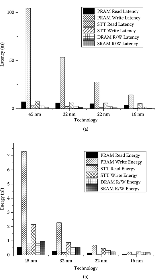
FIGURE 19.4 (a) Latency per access and (b) dynamic energy of different memory technologies at different technology nodes.
Figure 19.4 describes the effect of technology scaling on the dynamic energy and latency of different memory technologies. From Figure 19.4a, we see that SRAM has the lowest read latency at 45 nm and 32 nm, but for 22-nm and lower, the read latency of MRAM is comparable to that of SRAM. In terms of write latency, SRAM is the lowest for all technology nodes. The write latency for MRAM does not scale much and the write latency of PRAM scales according to the 1/k2 scaling rule. So, at lower technology nodes, the PRAM write latency is not that high compared to the MRAM write latency. However, they are both higher than SRAM and so are less suitable for L1 cache unless a write-back buffer is possibly used as in [19,20].
From Figure 19.4b, we also see that in all the technology nodes, PRAM has the highest write energy while the write energy of SRAM is the lowest. For read energy, PRAM and MRAM always have lower energy consumption than DRAM and SRAM. The energy of PRAM and MRAM scale very fast compared to SRAM and DRAM; PRAM write energy scales even faster than MRAM due to the 1/k2 scaling rule of its write latency. PRAM has the lowest read energy at 45 nm, but read energy of MRAM drops faster with technology scaling, making it the lowest one for 32 nm and lower technology nodes. Among all the technologies, the leakage power of SRAM is the highest. CACTI simulation results show that at 32-nm technology, 2M SRAM has 10 times more leakage than 2M PRAM and 2M MRAM. This is because PRAM and STT-MRAM cells have very low leakage compared to SRAM cells. All of this implies that the use of SRAM in L2 cache will increase the overall power consumption, as will be demonstrated in Section 19.3.
19.3 Heterogeneous Memory Design
Most multiple level caches, which are integrated on chip with CPU, consist of two or three levels of SRAM-based caches with gradually increasing size. The last or the highest cache level tends to occupy a large on-chip silicon area, and thus incurs a significant amount of leakage power consumption. Emerging NVMs, such as PRAM and STT-MRAM, which have high data storage density and low leakage power, have been considered as promising replacements of SRAM in higher levels of memory hierarchy. However, the access latency, especially the write latency of these memories, is much longer than that of SRAM. Thus, while using emerging memories in high cache level (L2 or L3) can dramatically reduce the leakage power consumption, the instructions per cycle (IPC) remains constant or decreases slightly.
19.3.1 Case Study of Heterogeneous Memory
In this section, we analyze heterogeneous memory under the same area rule, that is, the competing memory technologies have the same area (instead of memory size or density). Accordingly, a 4 MB STT-MRAM has the same area as a 16 MB MLC PRAM or a 512 KB SRAM.
We consider three configurations with comparable total area: Config (i) 32 KB SRAM in L1 and 512 KB SRAM in L2, Config (ii) 32 KB SRAM in L1 and 4 MB MRAM in L2, and Config (iii) 32 KB SRAM in L1 and 16 MB MLC PRAM in L2. We use SimpleScalar 3.0e [21] and our extension of CACTI to generate the latency and energy of the different cache system configurations. All caches are 8-way with 64 bytes per block.
Figure 19.5 shows the average energy comparison of the three configurations in 45-nm technology for seven benchmarks, namely gcc, craft, and eon from SPEC2000 and sjeng, perlbench, gcc06, and prvray from SPEC2006. For each benchmark, the first bar corresponds to Config (i), the second bar corresponds to Config (ii), and the third bar corresponds to Config (iii). The energy values of Configs (ii) and (iii) are normalized with respect to that of Config (i). For all the benchmarks, Config (i) has the largest energy consumption. Config (iii) has the second largest energy consumption. Config (ii) has the lowest energy consumption, which is 70% and 33% lower than Config (i) and Config (ii). The leakage energy of Config (iii) is almost the same as that of Config (ii) because the leakage of STT-MRAM and PRAM are both very low. The high dynamic energy of Config (iii) results from the repeated read&verify process for programming intermediate states in MLC PRAM.
Figure 19.6 plots the normalized IPC of the three configurations for the same set of benchmarks. The IPC increase is modest; it increases by 8% for Config (ii) and by 11% for Config (iii). This increase is because for the same area constraint, large L2 cache reduces the L2 cache miss penalty. Thus from Figures 19.5 and 19.6, we conclude that Config (ii), which uses STT-MRAM, has the largest IPC improvement with the lowest energy consumption.
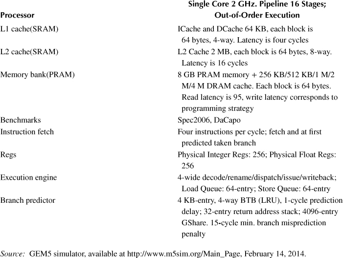
Next, we present an example of heterogeneous main memory design using a small-size DRAM as cache on top of large PRAM. The configurations used in GEM5 are listed in Table 19.3 [22]. Our workload includes the benchmarks of SPEC CPU INT 2006 and DaCapo-9.12. For the GEM5 simulations, the PRAM memory latency is obtained by CACTI and expressed in number of cycles corresponding to the processor frequency of 2 GHz.
Figure 19.7 shows the normalized IPC, lifetime, and energy of PRAM- and STT-MRAM-based heterogeneous main memory with different sized DRAM cache. The lifetime of PRAM is defined as the maximum number of program/erase (P/E) cycles for which data stored in memory remains reliable according to a 10−8 block failure rate (BFR) constraint. As the DRAM size of the PRAM-based heterogeneous memory increases, the frequency of PRAM access decreases and the lifetime of PRAM, in terms of P/E cycles, increases. The energy consumption has a significant reduction (about 50%) when cache size increases from 256 KB to 1M. That is because the amount of access to PRAM, which is costly in terms of high energy consumption, is reduced. However, the total energy consumption becomes flat as the cache size keeps increasing. This is because the reduction in PRAM energy due to very few accesses is offset by the increase in leakage and refresh energy of a large DRAM cache. Similar to IPC in heterogeneous cache design, the IPC of PRAM-based main memory increases slowly with increase in the size of DRAM cache. In general, if we want to achieve a balance between latency and energy, 1 M DRAM cache seems to be an efficient configuration. If long lifetime is also required, then the cache size should be increased though this does not result in much gain in performance and energy.
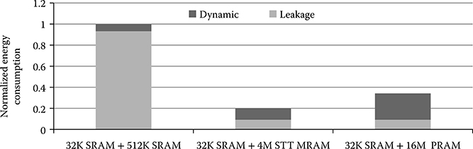
FIGURE 19.5 Normalized energy consumption of the three configurations for 45-nm technology. The normalization is with respect to Config (i).
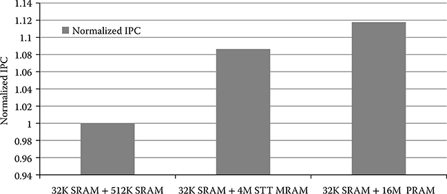
FIGURE 19.6 Normalized IPC (respect to Config (i)) of the three configurations for 45-nm technology. The normalization is with respect to Config (i).
Table 19.3 GEM5 System Evaluation Configuration
Source: GEM5 simulator, available at http://www.m5sim.org/Main_Page, February 14, 2014.
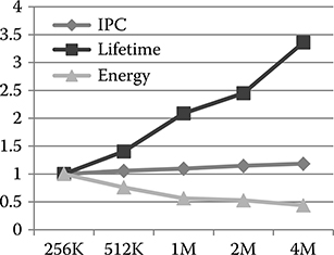
FIGURE 19.7 Normalized IPC, lifetime, and energy of PRAM-based heterogeneous main memory. The PRAM is of size 8 GB and the DRAM size is varied from 256 KB to 4 MB.
For STT-MRAM-based heterogeneous memory, the normalized lifetime and energy have the same trend as PRAM-based heterogeneous memory. That is because the reduction of accesses to the main memory is the same. The IPC improvement due to increased DRAM size is even lower than that in PRAM-based heterogeneous memory because the access latency of STT-MRAM is lower than that of PRAM, as shown in Figure 19.8.
19.3.2 Related Work
19.3.2.1 Heterogeneous Cache Architecture
In Chen et al. [23], STT-MRAM has been studied as the last-level (L2) cache to reduce cache leakage power. To address possible degradation in IPC performance, the NMOS transistor width of the access transistor is varied and the difference between read and write latency studied. Simulation results show that while some benchmarks favor the use of relatively small NMOS transistors in memory cells, others favor the use of relatively large NMOS transistors.
A relationship between retention time of STT-MRAM and its write latency has been established in Jog et al. [24] and used to calculate an efficient cache hierarchy. Compared to SRAM-based design, the proposed scheme lowers write latency and improves performance and energy consumption by 18% and 60%, respectively.
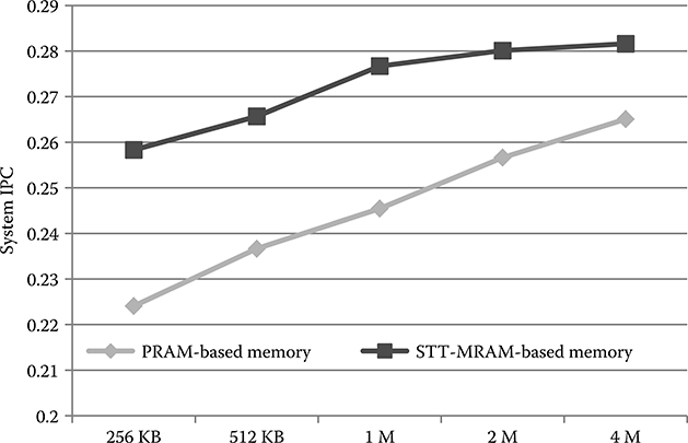
FIGURE 19.8 IPC of PRAM and STT-MRAM-based heterogeneous main memories. The DRAM size is varied from 256 KB to 4 MB.
Cache memories have also been designed where PRAM is used as L2 or the last level cache. In Joo et al. [25], design techniques are proposed to reduce the write energy consumption of a PRAM cache and to prolong its lifetime. This is done by using read-before-write, data inverting, and wear leveling. Simulation results show that compared with the baseline 4 MB PRAM L2 cache having less than an hour of lifetime, Joo et al. [25] achieved 8% of energy saving and 3.8 years of lifetime.
A novel architecture RHCA in which SRAM and PRAM/MRAM serve in the same cache level has been proposed in Wu et al. [26]. The PRAM/MRAM part is used to store data that is mostly used for reads and SRAM is used to store data that will be updated frequently. Because the read/write access ratio for a cache line changes over time, data is transferred from the fast SRAM region to the slow PRAM/MRAM region and vice versa dynamically.
19.3.2.2 Heterogeneous Architecture for Main Memory
Different memory combinations have been studied for the main memory level. Most of the work has been geared toward partially replacing DRAM, which has problems of large power consumption, especially due to refresh power and is not amenable to aggressive scaling. Unfortunately, PRAM has high programming energy and reliability problems. Thus, most approaches try to hide the write latency of PRAM and reduce the number of PRAM accesses by putting DRAM/Flash buffer or cache before PRAM-based main memory. The major differences among these architectures are memory organization, such as buffer/cache size or line size, and data control mechanisms.
An architecture where the DRAM is used as a buffer in a DRAM+PRAM architecture is proposed in Qureshi et al. [27]. The DRAM buffer is organized similar to a hardware cache that is not visible to the OS, and is managed by the DRAM controller. This organization successfully hides the slow write latency of PRAM, and also addresses the endurance problem of PRAM by limiting the number of writes to the PRAM memory. Evaluations showed that a small DRAM buffer (3% the size of PRAM storage) can bridge the latency gap between PRAM and DRAM. For a wide variety of workloads, the PRAM-based hybrid system provides an average speed up of 3X while requiring only 13% area overhead.
There are several DRAM+PRAM hybrid architectures where DRAM is used as cache. The architecture in Park et al. [28] uses DRAM as a last level cache. The DRAM can be bypassed when reading data from PRAM with the low cache hit rate. In this case, DRAM has lower refresh energy while the miss rate increases. Dirty data in DRAM is kept for a longer period than clean data to reduce the write backs to PRAM. This memory organization reduces the energy consumption by 23.5%–94.7% compared to DRAM-only main memory with very little performance overhead.
Another hybrid architecture has been proposed in Ferreira et al. [29], which focuses on the lifetime of PRAM. It achieves the same effect of lazy write by restricting CPU writes to DRAM and only writing to PRAM when a page is evicted. Such a scheme has been shown to have significant impact on endurance, performance, and energy consumption. Ferreira et al. [29] claim that the lifetime of PRAM can be increased to 8 years.
A PDRAM memory organization where data can be accessed and swapped between parallel DRAM and PRAM main memory banks has been proposed in Dhiman et al. [30]. To maintain reliability for PRAM (because of write endurance problem), Dhiman et al. [30] introduced a hardware-based book-keeping technique that stores the frequency of writes to PRAM at a page-level granularity. It also proposes an efficient operating-system-level page manager that utilizes the write frequency information provided by the hardware to perform uniform wear leveling across all the PRAM pages. Benchmarks show that this method can achieve as high as 37% energy savings at negligible performance overhead over comparable DRAM organizations.
19.4 Reliability of Nonvolatile Memory
One major drawback of NVMs is that they suffer from reliability degradation due to process variations, structural limits, and material property shift. For instance, repeated use of high currents during RESET programming of PRAM results in Sb enrichment at the contact reducing the capability of heating the phase change material to full amorphous phase and results in hard errors. Process variations in the metal–oxide–semiconductor field-effect transistor current driver in STT-MRAM impact the programming current and lead to unsuccessful switch. In order for NVMs to be adopted as a main part of heterogeneous memory, it is important that the reliability concerns of these devices also be addressed.
19.4.1 Reliability of Phase-Change Memory
As described in Section 19.2, the logical value stored in PRAM is determined by the resistance of the phase change material in the memory cell. Assuming there is no variation in the phase change material characteristic and there is no sense amplifier mismatch, the primary cause of errors in PRAM is due to overlap of the resistance distributions of different logical states, as shown in Figure 19.9a. The resistance distributions of all the states shift from the initial position due to the change in the material characteristics such as structure relaxation or recrystallization [31,32]. There are three threshold resistances, Rth (11,10), Rth (10,01), and Rth (01,00), to identify the boundaries between the four states. A memory failure occurs when the resistance distribution of one state crosses the threshold resistance; the error rate is proportional to the extent of overlap. Figure 19.9b shows the resistance distributions of state “00” obtained by using the parameters in Table 19.2 for running 10,000 point Monte-Carlo simulations. We see that the resistance distribution curve of state “00” has a long tail, which makes it more prone to error.
The reliability of a PRAM cell can be analyzed with respect to data retention, cycling endurance, and data disturbs [33]. For PRAM, data retention depends on the stability of the resistance in the crystalline and amorphous phases. While the crystalline phase is fairly stable with time and temperature, the amorphous phase suffers from resistance drift and spontaneous crystallization. Let data storage time (DST) be the time that the data is stored in memory between two consecutive writes. Then, the resistance drift caused due to DST can be modeled by
where Rt is the resistance at time t, RA is the effective resistance of amorphous part, Re is the effective resistance of crystalline part, and ν is the resistance drift coefficient, which is 0.026 for all the intermediate states. Note that RA and Re have different values for the different states. Soft errors occur when the resistance of a state increases and crosses the threshold resistance, demarcating its resistance state with the state with higher resistance.
Hard errors occur when the data value stored in one cell cannot be changed in the next programming cycle. There are two types of hard errors in SLC PRAM: stuck-RESET failure and stuck-SET failure [33]. Stuck-SET or stuck-RESET means the value of stored data in PRAM cell is stuck in “1” or “0” state no matter what value has been written into the cell. These errors increase as the number of programming cycles (NPC) increases.
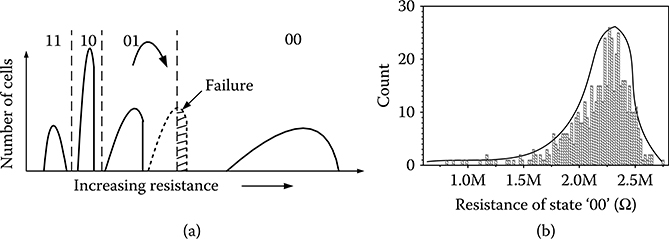
FIGURE 19.9 (a) An example of a failure caused by the “01” resistance shift. (b) Resistance distribution of the state “00.”
Stuck-SET failure is due to repeated cycling that leads to Sb enrichment at the bottom electrode [34]. The resistance reduction is a power function of the NPC and is given by ΔR = a × NPCb, where a equals 151,609 and b equals 0.16036 [35]. The stuck-SET failure due to the resistance drop of state “00” is the main source of hard errors in PRAM. This kind of errors occur if the resistance distribution of state “00” crosses Rth (00,01).
For MLC PRAM, the failure characteristics due to NPC is similar to that in SLC PRAM, but the number of hard errors in MLC PRAM is larger than that in SLC PRAM. This is to be expected since the threshold resistance between state “00” and state “01” in MLC PRAM is higher than the threshold resistance between state “0” and state “1” in SLC PRAM. As a result, for the same NPC, the number of errors due to distribution of state “00” crossing Rth (00,01) is higher.
In summary, hard error rate is determined by the resistance of state “00” decreasing and its distribution crossing Rth (01,00) and soft error rate is primarily determined by the resistance of state “01” increasing and its distribution crossing Rth (01,00). Thus, the threshold resistance Rth (01,00) plays an important role in determining the total error rate. Because we can estimate the resistance shift quantitatively, we can control the error rate by tuning the threshold resistance [35].
19.4.1.1 Enhancing Reliability of Phase-Change Memory
Many architecture-level techniques have been proposed to enhance the reliability of PRAM. Techniques to reduce hard errors in SLC PRAM have been presented in Qureshi et al., Seong et al., Schechter et al., and Yoon et al. [27,36–38]. Wear leveling techniques and a hybrid memory architecture that reduce the number of write cycles in PRAM have been proposed in Qureshi et al. [27]. The schemes in Seong et al. [36] and Schechter et al. [37] can identify the locations of hard errors based on read-and-verify process. While additional storage area is needed to store the location addresses of hard errors in Schechter et al. [37], iterative error partitioning algorithm is proposed in Seong et al. [36] to guarantee that there is only one hard error in a subblock so that it can be corrected during read operation. For correcting soft errors in MLC PRAM, a time tag is used in Xu et al. [39] to record the retention time information for each memory block or page and this information is used to determine the threshold resistance that minimizes the soft error bit error rate (BER). However, tuning of threshold resistance for reducing only soft errors has an adverse effect on its hard error rate. A multitiered approach spanning device, circuit, architecture, and system levels has been proposed for improving PRAM reliability [35,40]. At the device level, tuning the programming current profile can affect both the memory reliability as well as programming energy and latency. At the circuit level, there is an optimal threshold resistance for a given data retention time and number of programming cycles that results in the lowest error rate (soft errors + hard errors). At the architecture level, Gray coding and 2-bit interleaving distribute the odd and even bits into an odd block that has very low BER and an even block that has comparatively high BER. This enables us to employ a simpler error control coding (ECC) such as Hamming on odd block and a combination of subblock flipping [14] and stronger ECC on even block. The multitiered scheme makes it possible to use simple ECC schemes and thus, has lower area and latency overhead.
19.4.2 Reliability of Spin-Transfer Torque Magnetic Memory
The primary causes of errors in STT-MRAM are due to variations in MTJ device parameters, variations in CMOS circuit parameters, and thermal fluctuation. Recently, many studies have been performed to analyze the impact of MTJ device parametric variability and the thermal fluctuation on the reliability of STT-MRAM operations. Li et al. [41] summarized the major MTJ parametric variations affecting the resistance switching and proposed a “2T1J” STT-MRAM design for yield enhancement. Nigam et al. [42] developed a thermal noise model to evaluate the thermal fluctuations during the MTJ resistance switching process. Joshi et al. [43] conducted a quantitative statistical analysis on the combined impacts of both CMOS/MTJ device variations and thermal fluctuations. In this section, we also present the effects of process variation and geometric variation.
Typically, there are two main types of failures that occur during the read operation: read disturb and false read. Read disturb is the result of the value stored in the MTJ being flipped because of large current during read. False read occurs when current of parallel (antiparallel states) crosses the threshold value of the antiparallel (parallel) state. In our analysis, we find that the false read errors are dominant during the read operation; thus, we focus on false reads in the error analysis.
During write operation, failures occur when the distribution of write latency crosses the predefined access time. Write-1 is more challenging for an STT-MRAM device due to the asymmetry of the write operation. During write-1, access transistor and MTJ pair behaves similar to a source follower that increases the voltage level at the source of the access transistor and reduces the driving write current. Such a behavior increases the time required for a safe write-1 operation.
The variation impacts of the different parameters are presented in Figure 19.10 for read and write operations. To generate these results, we changed each parameter one at a time and did Monte Carlo simulations to calculate the contribution of each variation on the overall error rate. We see that variation in access transistor size is very effective in shaping the overall reliability; it affects the read operation by 37% and write operation by 44% with the write-0 and write-1 having very similar values. The threshold voltage variation affects the write operation more than the read operation. Finally, the MTJ geometry variation is more important in determining the read error rate as illustrated in Figure 19.10 [35].
19.4.2.1 Enhancing Reliability of Spin-Transfer Torque Magnetic Memory
The reliability of an STT-MRAM cell has been investigated by several researchers. While Joshi et al. [43] studied the failure rate of a single STT-MRAM cell using basic models for transistor and MTJ resistance, process variation effects such as RDF and geometric variation were considered in Chatterjee et al. [10] and Zhang et al. [44]. A methodology of optimizing STT-MRAM cell design that chose the MTJ device parameters and the NMOS transistor sizes to minimize write errors was proposed in Zhang et al. [18]. In Li et al. [41], an architecture-aware cell sizing algorithm that reduces read failures and cell area at the expense of write failures was proposed. In Yang et al. [14], we presented a multitiered approach spanning circuit level and system level to improve STT-MRAM reliability. By using a combination of an increase in the W/L ratio of the access transistor, applying a higher voltage difference across the memory cell, and adjusting pulse width in write operation, the error rate was significantly reduced. As a result, a low-cost ECC was able to achieve very low BFR.
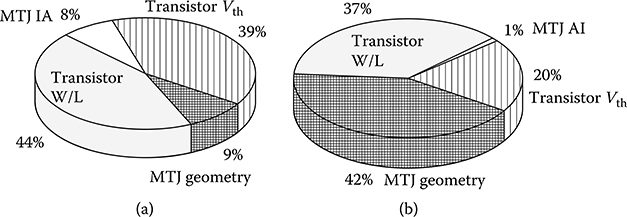
FIGURE 19.10 Effects of different variations on STT-MRAM. (a) Write operation. (b) Read operation.
We are not aware of any work that explicitly addresses the reliability of NVM-based heterogeneous memory systems. Existing DRAM + PRAM systems improve the reliability of PRAM implicitly by reducing the number of hard errors due to reduced number of P/E cycles. However, such a system is likely to see an increase in the number of soft errors because the time between two consecutive writes in the one PRAM page is larger. In this case, stronger ECC will be required to deal with increased soft errors that result in long decoding latency in read operation.
For STT-MRAM, programming current amplitude and width affect the probability of a successful write. To meet programming latency and energy constraints, a homogeneous memory system may have high error rate that has to be compensated by strong ECC. However, DRAM or SRAM buffer can also reduce the number of accesses to STT-MRAM, which would reduce the energy of the hybrid memory. In that case, the STT-MRAM part can still use high current pulse amplitude and long pulse width to achieve low error rate without adversely affecting the energy and latency performance of the system.
19.5 Conclusion
To address the scaling problems of CMOS-based memory devices in sub-nanotechnology and provide desirable performance, heterogeneous memory systems built with emerging memory technologies are needed. This chapter introduces a design methodology for such systems through device modeling, architecture level and system-level simulation, as well as reliability analysis. Compact device models of PRAM and STT-MRAM are built to facilitate study of memory latency, energy, and reliability. By embedding device model parameters into circuit and architecture simulators, system-level optimization can be achieved for different performance metrics. We also provide reliability analysis and methods to improve reliability for PRAM and STT-MRAM, because it affects memory energy, performance, and lifetime.
References
1. R. Venkatesan, V. J. Kozhikkottu, C. Augustine, A. Raychowdhury, K. Roy, and A. Raghunathan, “TapeCache: A high density, energy efficient cache based on domain wall memory,” ACM/IEEE International Symposium on Low Power Electronics and Design, pp. 185–190, 2012.
2. H. S. P. Wong, S. Raoux, S. Kim, J. Liang, J. P. Reifenberg, B. Rajendran, M. Asheghi, and K. E. Goodson, “Phase change memory,” Proceedings of the IEEE, pp. 2201–2227, December 2010.
3. G. W. Burr, M. J. Breitwisch, M. Franceschini, D. Garetto, K. Gopalakrishnan, B. Jackon, B. Kurdi et al., “Phase change memory technology,” Journal of Vacuum Science and Technology B, 28(2): 223–262, April 2010.
4. S. Thoziyoor, N. Muralimanohar, J. H. Ahn, and N. P. Jouppi, “CACTI 5.1 technical report,” HP Labs, Palo Alto, CA, Tech. Rep. HPL-2008-20, 2008.
5. X. Dong, N. Jouppi, and Y. Xie, “PCRAMsim: System-level performance, energy, and area modeling for phase-change RAM,” IEEE/ACM International Conference on Computer-Aided Design, San Jose, CA, pp. 269–275, 2009.
6. X. Dong, C. Xu, Y. Xie, and N. P. Jouppi, “NVSim: A circuit-level performance, energy, and area model for emerging nonvolatile memory,” IEEE Transactions on Computer-Aided Design of Integrated Circuits and Systems, 31(7): 994–1007, July 2012.
7. G. Sun, Y. Joo, Y. Chen, D. Niu, Y. Xie, Y. Chen, and H. Li, “A Hybrid solid-state storage architecture for the performance, energy consumption, and lifetime improvement,” IEEE 16th International Symposium on High Performance Computer Architecture, pp. 1–12, January 2010.
8. G. Dhiman, R. Ayou, and T. Rosing, “PDRAM: A hybrid PRAM and DRAM main memory system,” IEEE Design Automation Conference, San Francisco, CA, pp. 664–669, July 2009.
9. T. Kawahara, R. Takemura, K. Miura, J. Hayakawa, S. Ikeda, Y. Lee, R. Sasaki et al., “2 Mb SPRAM (spin-transfer torque RAM) with bit-by-bit bi-directional current write and parallelizing-direction current read,” IEEE Journal of Solid State Circuits, 43(1): 109–120, January 2008.
10. S. Chatterjee, M. Rasquinha, S. Yalamanchili, and S. Mukhopadhyay, “A scalable design methodology for energy minimization of STTRAM: A circuit and architecture perspective,” IEEE Transactions on VLSI Systems, 19(5): 809–817, May 2011.
11. Y. Chen, H. Li, X. Wang, W. Zhu, and T. Zhang, “A 130nm 1.2V/3.3V 16Kb spin-transfer torques random access memory with non-deterministic self-reference sensing scheme,” IEEE Journal of Solid State Circuits, pp. 560–573, February 2012.
12. Z. Xu, K. B. Sutaria, C. Yang, C. Chakrabarti, and Y. Cao, “Compact modeling of STT-MTJ for SPICE simulation,” European Solid-State Device Research and Circuits Conference, Bucharest, Romania, pp. 338–342, September 2013.
13. J. Kammerer, M. Madec, and L. Hébrard, “Compact modeling of a magnetic tunnel junction – Part I: dynamic magnetization model,” IEEE Transactions on Electron Devices, 57(6): 1408–1415, June 2010.
14. C. Yang, Y. Emre, Z. Xu, H. Chen, Y. Cao, and C. Chakrabarti, “A low cost multi-tiered approach to improving the reliability of multi-level cell PRAM,” Journal of Signal Processing, 1–21, DOI: 10.1007/s11265-013-0856-x, May 2013.
15. R. Annunziata, P. Zuliani, M. Borghi, G. De Sandre, L. Scotti, C. Prelini, M. Tosi, I. Tortorelli, and F. Pellizzer, “Phase change memory technology for embedded non volatile memory applications for 90nm and beyond,” IEEE International Electron Devices Meeting, Baltimore, MD, pp. 1–4, Dec. 2009.
16. G. Servalli, “A 45nm generation phase change memory technology,” IEEE International Electron Devices Meeting, Baltimore, MD, pp. 1–4, December 2009.
17. R. Dorrance, F. Ren, Y. Toriyama, A. Amin, C. K. Ken Yang, and D. Marković, “Scalability and design-space analysis of 1T-1MTJ memory cell,” IEEE/ACM International Symposium on Nanoscale Architectures, pp. 32–36, 8–9, June 2011.
18. Y. Zhang, X. Wang, and Y. Chen, “STT-RAM cell design optimization for persistent and non-persistent error rate reduction: A statistical design view,” IEEE Transaction on Magnetics, 47(10): 2962–2965, October 2011.
19. R. I. Bahar, G. Albera, and S. Manne, “Power and performance tradeoffs using various caching strategies,” International Symposium on Low Power Electronics and Design, Monterey, CA, pp. 64–69, August 1998.
20. B. Lee, E. Ipek, O. Mutlu, and D. Burger, “Architecting phase change memory as a scalable DRAM alternative”, International Symposium on Computer Architecture, pp. 2–13, June 2009.
21. Simplescalar 3.0e, available at http://www.simplescalar.com/, March 22, 2011.
22. GEM5 simulator, available at http://www.m5sim.org/Main_Page, February 14, 2014.
23. Y. Chen, X. Wang, H. Li, H. Xi, W. Zhu, and Y. Yan, “Design margin exploration of spin-transfer torque RAM (STT-RAM) in scaled technologies”, IEEE Transactions on Very Large Scale Integration Systems, 18(12): 1724–1734. December 2010.
24. A. Jog, A. Mishra, Cong Xu, Y. Xie, V. Narayanan, R. Iyer, and C. Das, “Cache revive: Architecting volatile STT-RAM caches for enhanced performance in CMPs,” Design Automation Conference, San Francisco, CA, pp. 243–252, June 2012.
25. Y. Joo, D. Niu, X. Dong, G. Sun, N. Chang, and Y. Xie, “Energy- and endurance-aware design of phase change memory caches,” Design, Automation and Test in Europe Conference and Exhibition, Dresden, Germany, pp. 136–141, March 2010.
26. X. Wu, J. Li, L. Zhang, E. Speight, and Y. Xie, “Power and performance of read-write aware Hybrid Caches with non-volatile memories,” Design, Automation & Test in Europe Conference & Exhibition, Nice, France, pp. 737–742, April 2009.
27. M. K. Qureshi, V. Srinivasan, and J. Rivers, “Scalable high performance main memory system using phase-change memory technology,” International Symposium on Computer Architecture, pp. 1–10, June 2009.
28. H. Park, S. Yoo, and S. Lee, “Power management of hybrid DRAM/PRAM-based main memory,” Design Automation Conference, New York, pp. 59–64, June 2011.
29. A. Ferreira, M. Zhou, S. Bock, B. Childers, R. Melhem, and D. Mosse, “Increasing PCM main memory lifetime,” Design, Automation & Test in Europe Conference & Exhibition, Dresden, Germany, pp. 914–919, March 2010.
30. G. Dhiman, R. Ayoub, and T. Rosing, “PDRAM: A hybrid PRAM and DRAM main memory system,” Design Automation Conference, San Francisco, CA, pp. 664–669, July 2009.
31. S. Lavizzari, D. Ielmini, D. Sharma, and A. L. Lacaita, “Reliability impact of chalcogenide-structure relaxation in phase-change memory (PCM) cells—Part II: physics-based modeling,” IEEE Transactions on Electron Devices, 56(5): 1078–1085, March 2009.
32. D. Ielmini, A. L. Lacaita, and D. Mantegazza, “Recovery and drift dynamics of resistance and threshold voltages in phase-change memories,” IEEE Trans. Electron Devices, 54(2): 308–315, 2007.
33. K. Kim and S. Ahn, “Reliability investigation for manufacturable high density PRAM,” IEEE 43rd Annual International Reliability Physics Symposium, pp. 157–162, 2005.
34. S. Lavizzari, D. Ielmini, D. Sharma, and A. L. Lacaita, “Reliability impact of chalcogenide-structure relaxation in phase-change memory (PCM) cells—Part I: Experimental Study,” IEEE Transactions on Electron Devices, pp. 1070–1077, May 2009.
35. C. Yang, Y. Emre, Y. Cao, and C. Chakrabarti, “Improving reliability of non-volatile memory technologies through circuit level techniques and error control coding,” EURASIP Journal on Advances in Signal Processing, 2012: 211, 2012.
36. N. H. Seong, D. H. Woo, V. Srinivasan, J. A. Rivers, and H. H. S. Lee, “SAFFER: Stuck-At-Fault Error Recovery for Memories,” Annual IEEE/ACM International Symposium on Microarchitecture, Atlanta, GA, pp. 115–124, 2009.
37. S. Schechter, G. H. Loh, K. Strauss, and D. Burger, “Use ECP, not ECC, for hard failures in resistive memories,” International Symposium on Computer Architectures, pp. 141–152, June 19–23, 2010.
38. D. H. Yoon, N. Muralimanohar, J. Chang, P. Ranganathan, N. P. Jouppi, and M. Erez, “FREE-p: Protecting non-volatile memory against both hard and soft errors,” IEEE 17th International Symposium on High Performance Computer Architecture, pp. 466–477, 2009.
39. W. Xu and T. Zhang, “A time-aware fault tolerance scheme to improve reliability of multi-level phase-change memory in the presence of significant resistance drift,” IEEE Transactions on Very Large Scale Integration Systems, 19(8): 1357–1367, June 2011.
40. C. Yang, Y. Emre, Y. Cao, and C. Chakrabarti, “Multi-tiered approach to improving the reliability of multi-level cell PRAM,” IEEE Workshop on Signal Processing Systems, Quebec City, pp. 114–119, October 2012.
41. J. Li, P. Ndai, A. Goel, S. Salahuddin, and K. Roy, “Design paradigm for robust spin-torque transfer magnetic RAM (STT MRAM) from circuit/architecture perspective,” IEEE Transactions on Very Large Scale Integration Systems, 18(12): 1710–1723, 2010.
42. A. Nigam, C. Smullen, V. Mohan, E. Chen, S. Gurumurthi, and W. Stan, “Delivering on the promise of universal memory for spin-transfer torque RAM (STT-RAM),” International Symposium on Low Power Electronics and Design, Fukuoka, Japan, pp. 121–126, August 2011.
43. R. Joshi, R. Kanj, P. Wang, and H. Li, “Universal statistical cure for predicting memory loss,” IEEE/ACM International Conference on Computer-Aided Design, San Jose, CA, pp. 236–239, November 2011.
44. Y. Zhang, Y. Li, A. Jones, and Y. Chen. “Asymmetry of MTJ switching and its implication to STT-RAM designs,” In Proceedings of the Design, Automation, and Test in Europe, Dresden, Germany, pp. 1313–1318, March 2012.