
8 Quest for Energy Efficiency in Digital Signal Processing
Architectures, Algorithms, and Systems
Ramakrishnan Venkatasubramanian
Contents
8.2 DSP Computing: Compute and Memory Bandwidth Trends
8.2.2 High-Performance Computing and DARPA Computing Challenges
8.3 DSP Comparison with Application Processors and GPU
8.3.1 What Makes a DSP a DSP? Real-Time Processing–DSP versus Application Processor
8.3.4 Single Core versus Multicore
8.4 DSP Compute Scaling Trend and Floating-Point Convergence
8.4.2 Fixed versus Floating Point
8.4.3 Dynamic Range and Precision
8.4.4 Convergence of Fixed and Floating Point
8.5 Energy Efficiency as the Metric
8.5.1 Gene’s Law and Its Scaling
8.5.2 Computational Density per Watt
8.6 Improving Energy Efficiency in Memory and IO Interfaces
8.6.1 Improving Memory Bandwidth and Memory Efficiency
8.7 Holistic Approach to DSP Processing: Architecture, Algorithms, and Systems
8.7.1 Algorithms Mapping to Underlying Architecture
8.7.2 Reducing IDLE and Standby Power
8.1 Introduction
Digital signal processors (DSPs) are essential for real-time processing of real-world digitized data, performing the high-speed numeric calculations necessary to enable a broad range of applications—from basic consumer electronics to sophisticated industrial instrumentation. Software programmability for maximum flexibility and easy-to-use, low-cost development tools of DSPs enable designers to build innovative features and differentiate value into their products, and get these products to market quickly and cost-effectively.
A modern-day MacBook Air operated at the energy efficiency of computers from 1991 would last only 2.5 seconds on its fully charged battery [1]. Technology scaling and architectural improvements have enabled tremendous energy efficiency in end products with the energy efficiency revolution over last three decades. The compute and memory bandwidth trends are only pointing us to improved computing and memory bandwidth requirements to enable rich and sophisticated user experience in handheld devices and the server platforms in the future.
8.2 DSP Computing: Compute and Memory Bandwidth Trends
In 2008, 68% of all DSPs were used in the wireless sector—mobile handsets and base stations [2]. A large percentage of the remaining 32% find usage in embedded systems—cameras, sensors, audio players, and industrial and automotive systems. Baseband chips typically consist of one or more DSP cores. The largest market for DSP silicon is known as embedded solutions, generally referred to as System-on-Chip (SoC) products. Of that SoC DSP market, cell phones constitute the largest segment, with baseband modem chips being the most significant. In 2012, Qualcomm shipped 616 million Mobile Station Modem chips. An average of 2.3 DSP cores in each chip amount to a total of 1.6 billion DSPs shipped in silicon in 2013 [3].
The energy efficiency of embedded SoCs in handheld and base station space has led to adoption of DSPs in the high-performance computing (HPC) space as coprocessors that offer increased giga floating-point operations per second per milliwatt (GFLOPS/mW) to enable energy-efficient scaling in the HPC domain.
The fundamental difference between handheld devices and HPC is the power versus performance trade-off in the overall power budget of the system. Handheld devices (cell phones, tablets, etc.) being battery operated are extremely sensitive for standby power. They try to optimize leakage and dynamic power of the embedded SoC to the fullest extent possible using hardware techniques such as automatic voltage scaling (AVS) and many hardware–software codesign techniques to reduce overall power. On the other hand, HPC kernels operate on large datasets and need the maximum performance possible in a given power budget. The design parameters are optimized differently to achieve the optimal solution to the HPC market. DSPs are broadly categorized into following three categories [4]:
Application-specific DSP (AS-DSP): Typically customized to an application to serve high-end application performance or cost requirements, for example, DSP optimized for speech coding.
Domain-specific DSP (DS-DSP): DS-DSPs are targeted to a wider application domain, for example, cellular modems (TI C540, TCSI Lode). They can be applied to a variety of applications within the domain and can run domain-specific algorithms efficiently.
General purpose DSP (GP-DSP): GP-DSP is designed for markets with a volume high enough to allow specialized solutions. GP-DSPs have evolved from the classic Fast Fourier Transform (FFT)/filtering multiply-accumulate design paradigm. Examples are TI C66x, Lucent 16xx, and ADI 21. GP-DSPs are readily available, widely applicable and have a large software base.
The industry trend is to increase compute capacity by using heterogeneous processing, using dedicated processing elements to efficiently handle specific tasks, and using high level of concurrency and parallelism to get the job done faster. Memory access latency has been the bottleneck for computing as the processor advances, the processing speed is usually input-output (IO) bound that the data is not ready when core needs it. Industry trend is to improve the efficiency of data movement, by prefetching the data closer to CPU, using wider memory bandwidth to reduce the memory access latencies. The compute and memory bandwidth trends are explained in the context of two domains—mobile computing and high-performance computing.
8.2.1 Mobile Computing Trends
The mobile computing and bandwidth trend in smartphones and tables is illustrated in Figure 8.1. The 1080p video support and octa-core (8 cores) already available in smartphones today [5] illustrate the compute trend in smartphones and tablets over the last decade. A smartphone has more computing power than personal computers and for the first time, the number of tablets and smartphones crossed the number of PCs in 2010 [6].
The compute power increase in tablets and smartphones enables richer end applications that find the need and use for all the compute power available in the system. But handheld devices being battery operated need to be extremely efficient to enable a long battery life. One of the most demanding applications where semiconductors are used is in the various applications of digital video from tablet computers to home entertainment. iPad with a retina display is already at high-definition (HD) resolution (2048 × 1536 pixels), and all indications are that video is racing toward what is known as 4K resolution, also known as ultrahigh definition, 3840 × 2160 pixels, which is roughly four times the pixels and hence four times as demanding as HD. A pictorial representation of display technology trend is shown in Figure 8.2 [7].
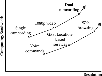
FIGURE 8.1 Mobile computing trends: Computing/bandwidth trend. (Woo, S. Samsung Analyst Day 2013, The Semiconductor Wiki Project, accessed August 2013, http://www.semiwiki.com/forum/files/S.LSI_Namsung%20Woo_Samsung%20System%20LSI%20Business-1.pdf.)
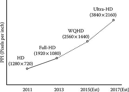
FIGURE 8.2 Mobile display trends: Illustrates memory bandwidth and compute trend. (Woo, S. Samsung Analyst Day 2013, The Semiconductor Wiki Project, accessed August 2013, http://www.semiwiki.com/forum/files/S.LSI_Namsung%20Woo_Samsung%20System%20LSI%20Business-1.pdf.)
Camera sensors are showing a similar exponential trend as well. This is illustrated in Figure 8.3. Very sophisticated image processing algorithms enable face detection, wide dynamic range, night vision, and other advanced features for processing the captured image in sensors.
8.2.2 High-Performance Computing and DARPA Computing Challenges
The end application for HPC is typically significant data crunching for scientific research or cloud-based data crunching on large data sets. Typically, HPC is used in oil and gas exploration, bioscience, big data mining, weather forecast, financial trading, electronic design automation, and defense. HPC systems need to be scalable, provide high computing power to meet the ever increasing processing needs with high energy efficiency for varied end applications. One of the major challenges faced in supercomputing industry is its efforts to hit exascale compute level by the end of the decade. In 1996, Intel’s Accelerated Strategic Computing Initiative (ASCI) Red was the first supercomputer built under the ASCI; the supercomputing initiative of the U.S. government to achieve 1 TFLOP performance [8]. In 2008, the IBM-built Roadrunner supercomputer for Los Alamos National Laboratory in New Mexico reached the computing milestone of 1 petaflop by processing more than 1.026 quadrillion calculations per second; it ranked number 1 in the TOP500 list in 2008 as the most powerful supercomputer [9]. Moving to 1000 times capacity to ExaFLOPs is very challenging—given the fact that power density of such ExaFLOP cannot expand 1000 times. Power delivery and distribution create significant challenges. Intel, IBM, and HP, for example, are continuing on the journey for core performance on multicore, many core, as well as graphical processing unit (GPU) accelerator model, and face significant power efficiency challenges.
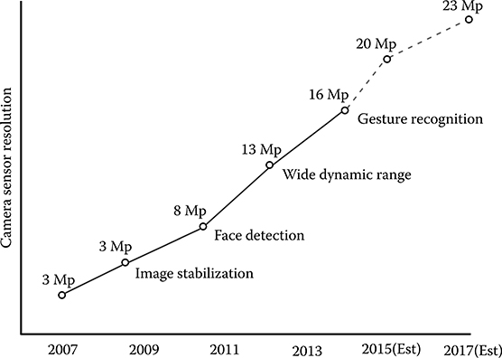
FIGURE 8.3 Mobile camera sensor trends: Illustrates memory bandwidth and algorithm trends. (Woo, S. Samsung Analyst Day 2013, The Semiconductor Wiki Project, accessed August 2013, http://www.semiwiki.com/forum/files/S.LSI_Namsung%20Woo_Samsung%20System%20LSI%20Business-1.pdf.)
To reach to the ExaFLOP level of compute performance, an optimal HPC processor should have sufficient compute performance and efficient data movement on chip and cross chips as necessary. The TOP500 list of supercomputers and their performance scaling is shown in Figure 8.4 [10]. Even in defense industry, most deployed military information systems have constrained computational capability because of limited electrical power available on platforms, heat dissipation challenges, and limitations in size and weight. The end result is that many of the current intelligence, surveillance, and reconnaissance systems have sensors that collect more information than can be processed in real time resulting in potentially valuable real-time intelligence data not processed in a timely manner.
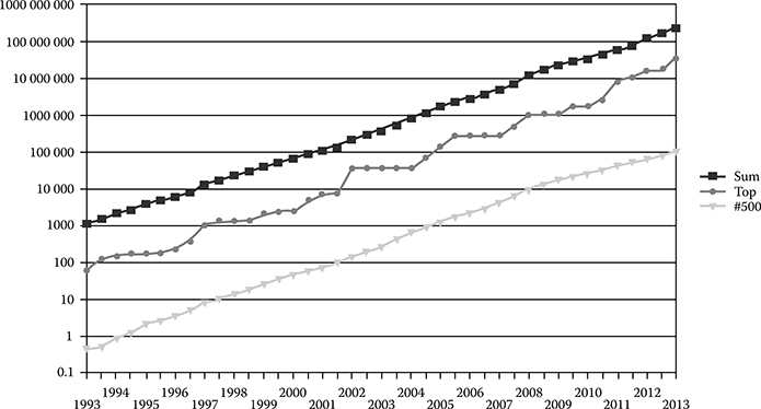
FIGURE 8.4 The logarithmic y axis shows performance in GFLOPS. The “Top” line denotes the fastest supercomputer in the world at the time. The “#500” line denotes supercomputer No. 500 on the TOP500 list. The “Sum” line denotes the total combined performance of supercomputers on the TOP500 list. (TOP500, Wikipedia, accessed August 2013, http://en.wikipedia.org/wiki/TOP500)
Current embedded processing systems have power efficiencies of around 1 GFLOPS/W. Recently, Texas Instruments multicore DSP claimed to achieve 12.8 single precision GFLOPS/W [11]. Warfighters anticipate requirements of at least 75 GFLOPS/W. The goal of the Power Efficiency Revolution For Embedded Computing Technologies (PERFECT) program is to provide warfighter-required power efficiency [12]. PERFECT aims to achieve the 75 GFLOPS/W goal by taking novel approaches to processing power efficiency. These approaches include near-threshold voltage operation and massive heterogeneous processing concurrency, combined with techniques to effectively use the resulting concurrency and tolerate the resulting increased rate of soft errors. To reach Defense Advanced Research Projects Agency (DARPA) PERFECT goals, it requires more than 14 times more power efficiency compared to current DSPs and 75 times more power efficiency comparing to typical HPC processors.
8.3 DSP Comparison with Application Processors and GPU
8.3.1 What Makes a DSP a DSP? Real-Time Processing—DSP versus Application Processor
A DSP is typically characterized by a single-cycle MAC (multiply and accumulate) operation and has the ability to support hard real-time requirements. They enable a better support for real-time requirement (e.g., audio samples delivered every 100 milliseconds and the signal processing has to be completed within that window to keep up with the real-time data stream) with short pipelines, in order processing, no speculation in the processor, ability to run a high-level real-time operating system (RTOS), low latency interrupts, and so on. Further, DSPs typically also support multiple execution units with highly customized datapaths, sophisticated direct memory access (DMA), and high-bandwidth memory systems, with very efficient zero or near-zero overhead looping.
In a hard real-time system, missing a deadline would result in a total system failure. In a soft real-time system, the usefulness of the results degrades after its deadline, thereby degrading the quality of service of the system.
An application processor provides high-level OS functions such as virtualization, multiple levels of caches with MMU, speculative fetching and branching, protected memory, semaphore support, context save and restore, and threading support. An application processor such as an ARM® core in an embedded SoC typically will not be able to meet hard real-time requirements, but might be able to support soft real-time requirements.
8.3.2 VLIW and SIMD
Very long instruction word (VLIW) architectures have multiple functional units that take advantage of vastly available instruction-level parallelism in applications. Single-instruction multiple data (SIMD) techniques operate on multiple data in a single instruction (exploiting data parallelism).
The main difference between DSP and other SIMD-capable CPUs is that the DSPs are self-contained processors with their own instruction set, whereas SIMD extensions rely on the general-purpose portions of the CPU to handle the program details, and the SIMD instructions handle the data manipulation only. DSPs also tend to include instructions to handle specific types of data, sound, or video, for instance, whereas SIMD systems cater to generic applications.
Oftentimes, a general purpose processor executes the main application and calls the SIMD processor for the compute-intensive kernels. SIMD has typically dominated HPC since Cray-1. Adding SIMD enhancements to embedded processing cores is becoming increasingly common as well. ARM® A15 cores offer SIMD instructions. The Texas Instruments C66x DSP architecture adds SIMD instructions to a VLIW architecture [11].
8.3.3 DSP versus GPGPU
A GPU provides more FLOPs per chip when compared to the x86 main processor in a computer. This raw GPU performance is achieved by the following reasons:
Each core inside the GPU is very simple, with a simple instruction set and no out-of-order, speculation, or other complex logic. Programming the GPU is more complicated, as programs are run on groups of processors and with lots of little constraints. This makes it possible to fit more cores into the same area.
GPUs typically have very little cache memory. Hence programs have to rely on bandwidth and managing to stream data the GPU.
A GPGPU (general-purpose GPU) extends usage of GPU units to general-purpose tasks. For tasks that operate on wide data (vector processing) and data intensive (imaging, video, graphics), GPGPU programming can offer predictable algorithms that can effectively and efficiently prefetch data and stream it through the cores at a predictable rate. But GPGPUs are very bad for control code programming. SIMD processing is applied on large vectors of independent elements in parallel.
A classic single-core DSP, on the other hand, has specialized instructions in the instruction set for signal processing, support for loops in very efficient ways, and is often SIMD. Recent DSP implementations support vector processing capabilities as well. DSPs are general enough to be able to run a rudimentary OS and operate semi-independently from the main processor. In a multicore DSP cluster, each DSP operates on a different problem. So rather than one vector of a thousand elements in a video compression, each DSP might operate on independent video streams load balancing all the thousand streams across the multicore cluster. Although DSP programming is painful compared to GP processors, their programming model is much simpler compared to GPGPUs [13]. Hence, GPGPUs are very different from DSPs and are used to solve different types of problems in different ways.
8.3.4 Single Core versus Multicore
The trend to develop multicore systems is a general trend not just in DSPs but across the processor space. The thermal design power limitations and the energy efficiency requirements have forced processor developers to add multicore capabilities instead of increasing the clock frequency of the operation.
The variable parameters in the design of multicore systems include type and number of cores; the speed of operation of the cores (instances required); homogeneous or heterogeneous multicore systems; and the usual considerations of area, power, and performance.
Functions that determine the topology and architecture of a multicore platform are cache coherency and memory bandwidth. When there are caches involved in a multicore system, support for cache coherency across the entire multicore system is desired as it enables the software running on the embedded processing system to balance load and allocate tasks seamlessly between cores. In addition to the number of cores, the reduced instruction set computer (RISC) (control decision)/SIMD (data vector) processing balance for the end application determines the number of DSP or application processors required in the system. Specialized hardware accelerators typically improve specific algorithms in hardware by a factor of 10×–50× over a GPCPU or DSP. Availability of such specialized accelerators improves the overall energy efficiency of the system by powering up the accelerator logic only for the duration it is required. It also frees up available compute capability in the multicore system for other processing. High-bandwidth sophisticated DMA functions take up all the data movement tasks in the multicore platform, enabling processors to be powered up on demand for a specific data processing task. Further, the software programming model, the software tool chain availability, and support for multicore programming models, such as OpenMP, are typically taken into account in the selection of multicore architectures for a given end application.
8.4 DSP Compute Scaling Trend and Floating-Point Convergence
8.4.1 GMAC Scaling Trend
GMAC is a one billion multiply-accumulate operations. The metric for measuring the performance improvement in DSPs is GMAC scaling. Figure 8.5 shows the MMAC/s (million multiply-accumulate operations per second) trend over five generations of Texas Instruments DSP architectures [14]. The MMAC improvement trend attributed to both the clock increase and parallel processing across generations shows that MMAC availability in DSP cores double every year. It can be seen that within the same architecture, technology scaling typically improves performance by a factor of two. On top of technology scaling, architectural improvements enhance performance by another factor of two. Although the MMAC compute scaling trend enables significant compute scaling, the focus has since shifted to energy efficiency.
8.4.2 Fixed versus Floating Point
There are many considerations for system developers when selecting DSPs for their applications. Among the key factors to consider are the computational capabilities required for the end application, processor and system costs, performance attributes, and ease of development. The first and foremost factor is the fixed-point versus floating-point arithmetic support for the end application.
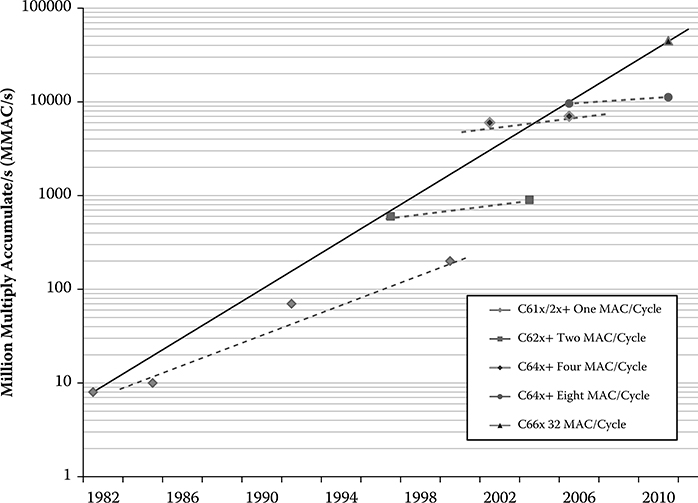
FIGURE 8.5 TI DSP MMAC scaling over the last 30 years. The dotted lines show the performance of each architecture with improvement achieved by technology scaling. The performance shift between dotted lines shows the impact of the architectural innovations between successive architectures. (R Venkatasubramanian, Texas Instruments, Inc., Dallas, TX.)
Underlying DSP architecture can be separated into two categories based on the numeric representation—fixed point and floating point. These designations refer to the format used to store and manipulate numeric representations of data [15].
Fixed-point systems use the bits to represent a fixed range of values, either integers or with a fixed number of integer and fractional bits. The dynamic range of values is therefore quite limited and values outside the set range must be saturated to the endpoints. Fixed-point processors usually quote their 16-bit performance as multiplies per second or MAC operations per second. Algorithms developed for fixed-point processors have to operate on a set of data that stays within the predetermined range to make the optimal use of the quoted DSP performance. Because of this, any data set that is not predictable or has a wide variation will have significant performance reduction in a fixed-point DSP.
On the other hand, floating-point representations offer a wider dynamic range by rational number representation (scientific notation), using a mantissa and an exponent for the representation. Floating-point representation was standardized by the IEEE Standard for Floating-Point Arithmetic, IEEE 754. It is a technical standard for floating-point computation established in 1985. The latest version, IEEE 754-2008 published in August 2008, extends the original IEEE 754-1985 standard and IEEE Standard for Radix-Independent Floating-Point Arithmetic, IEEE 854-1987. Single-precision floating-point format is represented in 4 bytes (32 bits) and represents a wide dynamic range of floating-point values. Double-precision floating-point format is represented by 8 bytes (64 bits) and represents an even wider dynamic range of floating-point values.
Single-precision floating-point operations where numbers are represented in 32 bits as: (−1)5 × M × 2(N − 127), where S is the sign bit, M the mantissa, and N the exponent. S is 1 bit, N represented in 8 bits and M represented with 23 bits. In this way numbers in the range 2−127 − 2128 can be represented with 24 bits of precision in the mantissa. By contrast, a fixed-point algorithm with 16 bits can only represent a range of 216 values (the numbers 0–65535), so there is much less dynamic range inherent in the numerical representation. Hence, any data set that is not predictable or has a wide variation would naturally fit into a floating-point representation of the data set.
8.4.3 Dynamic Range and Precision
The exponentiation inherent in floating-point computation assures a much larger dynamic range—the largest and smallest numbers that can be represented—which is especially important when processing extremely large data sets or data sets where the range may be unpredictable. As such, floating-point processors are ideally suited for computationally intensive applications.
It is also important to consider fixed- and floating-point formats in the context of precision—the size of the gaps between numbers. Every time a DSP generates a new number via a mathematical calculation, that number must be rounded to the nearest value that can be stored via the format in use. Rounding and/or truncating numbers during signal processing naturally yields quantization error, which is the deviation between actual analog values and quantized digital values. Since the gaps between adjacent numbers can be much larger with fixed-point processing when compared to floating-point processing, round off error can be much more pronounced. As such, floating-point processing yields much greater precision than fixed-point processing, thereby distinguishing floating-point processors as the ideal DSP when computational accuracy is a critical requirement.
The data set requirements associated with the target application typically dictate the need for fixed-point or floating-point processing.
8.4.4 Convergence of Fixed and Floating Point
From a hardware implementation point of view, fixed-point implementations are definitely smaller and faster than floating-point implementations. However, there is a price to pay in terms of development time for certain algorithms. Typically, algorithms are developed based on computer models and used for initial system deployments. As the deployments grow in scope and usage, engineers gather real-world data and bring this back to the lab to improve the system performance by tweaking the algorithms. These new algorithms are often developed using MATLAB® or other inherently floating-point tools. The challenge then lies in translating these floating-point algorithms to fixed-point algorithms while retaining the performance of both the algorithm and of the system. Unwieldy or complex algorithms can use up a disproportionate amount of system resources thereby lowering the overall performance of the system. It is not uncommon for the process of porting code from MATLAB to a real system to take weeks or months when complicated processing is involved. If the DSP processor hardware offers floating-point support, the entire conversion from floating point to fixed point is unnecessary and would enable faster time to market. This is illustrated in Figure 8.6 [15].
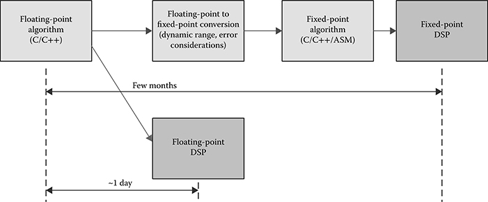
FIGURE 8.6 Effort involved in fixed-point to floating-point conversion and ease of mapping to floating-point DSP.
Across mission-critical applications, such as defense, public safety infrastructure, and avionics, floating point provides ease of development and performance lift. Not only does floating point shorten development life cycle by being able to use code directly out of MATLAB, but also floating-point implementations of many algorithms take fewer cycles to execute than fixed-point code (such as large FFT). For example, radar, navigation, and guidance systems process data that are acquired using arrays of sensors. The varying energy pattern across the many sensor elements provides the information relevant to the location and tracking of the target. This array of data must be processed as a set of linear equations to extract the desired information. Solution methods include math functions such as matrix inverse, factorization, and adaptive filtering. Image recognition, used for medical imaging such as ultrasound, as well as machine vision and industrial automation, also requires a high degree of accuracy and thus benefits from floating point. In ultrasound, signals from sound sources must be defined and processed to create output images that provide useful diagnostic information. The greater precision enables imaging systems to achieve a much higher level of recognition and definition for the user.
A well-known application area for floating-point use is in audio processing, where a high sampling rate, coupled with very tight latency requirements, can force filtering and other noise reduction algorithms toward the higher precision and larger dynamic range provided by floating point. Wide dynamic range also plays a part in robotic design. Unpredictable events can occur on an assembly line. The wide dynamic range of a floating-point DSP enables the robot control circuitry to deal with unpredictable circumstances in a predictable manner.
Texas Instruments introduced the C66x line of DSP processors in 2009, which merged fixed- and floating-point capabilities into a single processor without compromising the speed of operation [11]. Since then, almost all the major players in the DSP market space have followed suit and merged fixed-/floating-point implementations in their DSPs.
8.5 Energy Efficiency as the Metric
8.5.1 Gene’s Law and Its Scaling
According to Gene’s law [16], the power dissipation in embedded DSP processors reduces by half every 18 months. One metric that has been used to illustrate this scaling is “mW/MIPS.” Figure 8.7 shows the mW/MIPS trend with respect to DSP processor improvements over multiple decades. Of course, the driving force for Gene’s law has been all the computational requirements for various end applications as described in Section 8.2. Some of the metrics used for comparison of DSP architectures include computational density per watt (CDW) and energy per function.
8.5.2 Computational Density per Watt
In computing domain, CDW is a measure typically used to determine the energy efficiency of a particular computer architecture or system. Computational density is the measure of computational performance across range of parallelism, grouped by process technology [17]. CDW normalizes the process technology and process voltage considerations and provides a single metric that can be used to compare performance across range of parallelism.
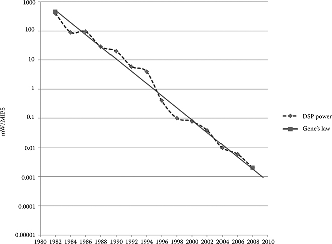
FIGURE 8.7 Gene’s law. (Frantz, G., Digital signal processor trends, IEEE Micro, 20(6), 52–59, © 2000 IEEE.)
In the context of DSP cores, the CDW metric that is typically used is the number of MMAC’s supported by 1 milliwatt of power (MMAC/mW). Based on the type algorithms running in the end application, the exact computational unit is compared for CDW. Example: In HPC, the majority of the operations are double precision floating-point operations. So the number of double-precision floating-point per watt is the metric used in HPC. Other typical computational metrics include 16-bit integer per watt, 32-bit integer per watt and single-precision floating-point per watt.
Sometimes computational density is normalized to energy. In such scenarios, energy efficiency metric (MMAC/mJ) is used for comparison. Typically, all the architectural and physical design innovations in DSP design are targeted toward improving the overall power and energy efficiency of the overall system. For example, the C66x DSP core from Texas Instruments [14] showed a power efficiency improvement of 4.5× over the previous C64x+ DSP architecture as shown in Table 8.1.
8.5.3 Energy per Function
If an algorithm is predominantly using one type of function (e.g., 1024-point single-precision FFT), the exact energy for that function can be computed for diverse architectures and “Energy per function” metric can be used for comparing the architectures. Note that “Energy per function” is different from the “Energy efficiency per watt” metric. Energy efficiency per watt computes total energy consumed regardless of the end algorithm or function, whereas energy per function only looks at one function and computes the energy for the same. For example, in HPC, FFT’s are used widely. A comparison of “Energy per FFT function” between GPU, DSP, and GPP is shown in Table 8.2 [18].
Table 8.1 TI DSP Power Efficiency Scaling
|
C64x+ (2005) |
C66x (2009) |
Comments |
Process and voltage |
65 nm, 1.1 V |
40 nm, 1 V |
|
Operating speed |
1GHz |
1.25 GHz |
|
Total power |
960 mW |
1180 mW |
|
16-bit fixed-point MMAC |
8000 |
40000 |
|
Power efficiency (MMAC/mW) |
8.3 |
37 |
4.5X improvement |
Source: Damodaran, R. et al., 25th International Conference on VLSI Design (VLSID) ©2012 IEEE.
Table 8.2 Energy per FFT Function
Platform |
Effective Time to Compute 1024 Point Complex-to-Complex Single-Precision FFT (μS) |
Power (W) |
Energy per FFT (μJ) |
GPU: nVidia Tesla C2070 |
0.16 |
225 |
36.0 |
GPU: nVidia Tesla C1060 |
0.30 |
188 |
56.4 |
GPP: Intel Xeon Core Duo @3 GHz |
1.80 |
95 |
171.0 |
GPP: Intel Nehalem Quad core @3.2 GHz |
1.20 |
130 |
156.0 |
DSP: TI C6678 @1.2 GHz |
0.86 |
10 |
8.6 |
Source: Saban N. Multicore DSP vs. GPUs, Workshop on GPU & Parallel Computing, Israel, January 2011, http://www.sagivtech.com/contentManagment/uploadedFiles/fileGallery/Multi_core_DSPs_vs_GPUs_TI_for_distribution.pdf.
8.5.4 Application Cube
Another interesting metric for DSP architecture comparison called “Application cube” was proposed by Lucent back in 1997 [19]. It is shown in Figure 8.8. The three parameters—power, performance, and cost—are defined on the axes of the cube in three dimensions. For any particular application, each DSP processor is mapped to various cubes and smaller the volume of the cube, the more suited the DSP is to the application. Ever since this metric was proposed in 1997, code size has become less important consideration, and the dimension could instead be replaced with “Memory bandwidth per function.”
8.5.5 Energy Benchmarking
Benchmark suites such as BDTI [20] and EEMBC® [21] are typically used for performance and power analysis and comparison across architectures. However, benchmarking multicore architectures are significantly more complicated than benchmarking single-core devices. This is because multicore performance is not only affected by the choice of CPU, but also is heavily dependent on the memory system and the interconnect capabilities [2].
Depending on the end application, specific application kernels are used for benchmarking as shown in Table 8.3. Even though different architectures may show different results for the application kernels, finally what matters is the actual performance achieved for the system in the context of the end application.
Because of the focus on energy efficiency and power efficiency considerations in architectures, EEMBC released EnergyBench™ [21]—a benchmark suite that attempts to provide data on the amount of energy a processor consumes while running EEMBC’s performance benchmarks. The EEMBC-certified Energymark™ score is a metric that normalizes the process technology and voltage and provides a metric for a processor’s efficient use of power and energy.
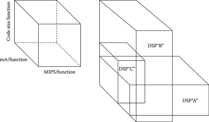
FIGURE 8.8 Application cube. (Edwin J. Tan and Wendi B. Heinzelman, DSP architectures: past, present and futures, SIGARCH Comput. Archit. New, 31(3), 6–19, http://doi.acm.org/10.1145/882105.882108, © 2003 IEEE.)
Table 8.3 Typical Benchmarks for Various Application Classes
Type of Application |
Typical Algorithms |
Control code |
Loops, calls and returns, branch performance |
Multimedia and graphics kernels |
SAD, DCT/IDCT |
General DSP |
FFT, IFFT, IIR, matrix multiply, viterbi decoding |
Application specific |
Mediabench for multimedia, radar algorithms for RADAR etc. |
8.6 Improving Energy Efficiency in Memory and IO Interfaces
8.6.1 Improving Memory Bandwidth and Memory Efficiency
On-chip embedded SRAM has been an area of active research for the last three decades. In advanced technology nodes, numerous power management techniques have been used to improve memory energy efficiency including memory pipelining to enable full bandwidth from memories and array source biasing [14]. Near-threshold operation of memories with assist circuits has been deployed to reduce the overall memory leakage power as well.
For external memory accesses, the access latency has become a major performance road block in recent years as memory performance has not kept up with the processing capacity gains from CPU frequency and massive parallelism in multi-core SoCs. Next-generation high-performance memory interfaces such as Hybrid Memory Cube (HMC) and High-Bandwidth Memory Interface (HBM) are being looked at to address the memory performance bottleneck.
HMC is a computer RAM technology developed by Micron Technology that deploys 3D packaging of multiple memory dies, typically 4 or 8 memory dies per package with through-silicon vias (TSV) and microbumps [22]. It has more data banks than classic DRAM memory of the same size, and memory controller is integrated into memory package as separate logic die. According to the first public specification HMC 1.0, published in April 2013, HMC uses 16-lane or 8-lane (half-size) full-duplex differential serial links, with each lane having 10, 12.5, or 15 Gbps SerDes. The ultimate aim of HMC memory topology is to offer improved Gbps data transfer at a lower power footprint.
A standard that leverages Wide IO and TSV technologies to deliver products with memory interface ranging from 128 GB/s to 256 GB/s has been defined by the HBM initiative by JEDEC standard in March 2011 [23]. The HBM task group is defining support for up to 8-high TSV stacks of memory on a data interface that is 1024-bit wide. HBM provides very large memory bandwidth because of parallelism; it basically integrates memory into the same SoC package and thus increases processing capacity in the SoC and reduces the power per Gbps compared to HMC.
8.6.2 High Bandwidth IOs
Consider a multicore SoC with some number of DSP cores and application processor cores (and potentially multimedia and other accelerator peripherals). For efficient processing in the cores in the SoC, enough data movement has to be enabled in and out of the SoC to feed the computational capacity offered by the cores. Figure 8.9 gives an overview of IO interfaces that can potentially be used in an embedded multicore SoC with their relative latency versus bandwidth comparison [23,24]. On one end of the spectrum is the high bandwidth applications support with 1 or 10 Gigabit Ethernet interfaces that enable data transfer over a long distance. On the other end of the spectrum, we have PCI Express and other serial interfaces that offer short links with high data rates. Each of the categories of interfaces is evolving and continues to offer the most efficient data transfer at the least power footprint depending on the end-use case. It is important to note that getting data in and out of the multicore SoC takes up significant amount of energy and the SoC architecture has to comprehend this.
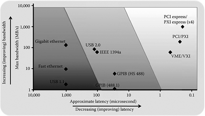
FIGURE 8.9 IO bandwidth versus latency comparison. (From National Instruments white-paper, PXI Express Specification Tutorial, 2010, http://www.ni.com/white-paper/2876/en/.)
8.7 Holistic Approach to DSP Processing: Architecture, Algorithms, and Systems
8.7.1 Algorithms Mapping to Underlying Architecture
AS-DSP and DS-DSP described in Section 8.2 typically would be tailored to a specific market. For example, Qualcomm’s Snapdragon processor is tailored for a specific market—application processor for mobile application. The architecture is tailor made for individual functions in that application space. Similarly, a processor optimized for audio/voice domain would require a much lower power and smaller footprint DSP.
Depending on the application, loss of precision and dynamic range due to floating-point to fixed-point conversion can be avoided by choosing processor cores with native floating-point support. This results in improved time to market and better dynamic range for calculations. For every algorithm in the application space, the mapping of the algorithm to the underlying architecture is key to achieving the most energy efficient end product out of the architecture. The energy per function and the CDW metrics for the specific functions need to be compared and the architecture/algorithms optimized accordingly to enable energy efficiency improvement. Data movement within the SoC and to/from external sources consumes power and energy. This should be factored in mapping of DMA and processor assignment for tasks in a multicore system.
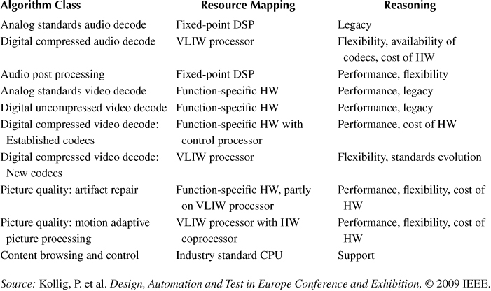
For multimedia end applications, Kollig et al. [25] describe the process that is typically followed to map all the functions in the application kernel to the available heterogeneous multicore resources and be able to maximize the energy efficiency of the system. Table 8.4 shows a potential mapping of algorithm class to the resources available in the SoC.
For voice activation application in a smartphone, the power consumption linked with three different architectures is shown below:
Voice activation on ARM® A9 (application processor) takes about 20 mA.
Using a dedicated chip for handling always-on voice processing, using TI C55 (GP-DSP), the consumption reduces to 4.5 mA.
Voice activation on CEVA TL410, the Teak Lite DSP core (AS-DSP) consumes less than 2 mA.
So depending on the end application and the available resources, the power and energy consumption can vary significantly. This has to be taken into account in mapping of algorithms to available resources in an SoC.
8.7.2 Reducing IDLE and Standby Power
IDLE and Standby power is the leakage and dynamic power consumed when the processor core is not performing any active task. IDLE/Standby power management is typically achieved by either of the two implementation schemes:
Based on the load balancing and scheduling operations, software can use AVS implementation if it is available (on a per core granularity) to reduce the voltage of processor core that is idle.
Software can schedule all the data crunching activities to a given processor and enable completion of the task as soon as possible with full voltage and maximum clock frequency. Once the task is complete, the processor core can be powered down.
The decision metric to use either of the above schemes is the idle period. If the processor core is idle for a long period, powering it down would provide the most energy efficient solution. On the other hand, if the idle periods are short and happen more often, it may better qualify for automatic voltage scaling.
8.7.3 Architecture (Hardware Platform)
A general overview of multicore DSP platforms is provided by Karam et al. [2], Tan and Windi [26], and Oshana [27]. From an energy efficiency point of view, heterogeneous multicores offer the best algorithm mapping to the underlying architecture. Typically any end application has a control plane that requires application processing including high-level operating system tasks. The data plane is controlled by the control plane, which includes all the high-speed DMA functions and monitoring the data crunching operations in the DSP or GPU or hardware accelerators. High-speed IOs typically facilitate this high-speed data movement.
Table 8.4 Algorithm Mapping to Resources for a Multimedia SoC
Source: Kollig, P. et al. Design, Automation and Test in Europe Conference and Exhibition,© 2009 IEEE.
This heterogeneous multicore operation is illustrated in the context of the scalable multicore platform called Keystone from Texas Instruments [28]. The heterogeneous multicore platform is shown in Figure 8.10. Keystone multicore architecture supports a variable number of C66x floating-point DSP cores and ARM® Cortex A8 and A15 RISC cores. These programmable elements are supplemented by AccelerationPacs, which are configurable accelerators that offload standardized functions from the programmable cores. As the features are implemented in hardware, AccelerationPacs give significant performance improvement for the function with improved energy efficiency. Physical interconnection within the chip denoted by Teranet and Multicore Navigator offer structures for fast access to on-chip memory and to external memory and hardware-based feature to facilitate load balancing and resource sharing within and between chips. These elements are scalable, allowing the platform to tailor the SoC to the performance and power consumption needs of devices serving different markets. Finally, there are high-performance IOs which, like the AccelerationPac, vary by market.
The Keystone Multicore SoC enables three levels of compute capabilities:
DSP CorePac with vector processing performs the scientific, data crunching, delivers real-time low-latency analytics achieving 12.8 GFLOP/W power efficiency.
ARM® CorePac handling the control plane tasks including high-level OS support, task management, and protocol logic.
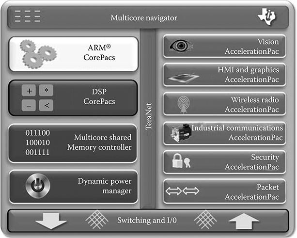
FIGURE 8.10 Keystone heterogeneous multicore platform from Texas Instruments. (From Texas Instruments Keystone Platform. http://www.ti.com/lsds/ti/dsp/keystone_arm/overview.page.)
Configurable and programmable AccelerationPac delivering fast-path data processing with low latency and deterministic response.
All these heterogeneous compute elements can run in parallel to achieve high capacity, power efficiency and delivers performance more than Moore’s law.
A few embedded processing SoCs that belong to this platform include:
TI 66AK2H12: 4 Cortex-A15 processors and 8 TMS320C66x DSPs optimized for HPC, media processing, video conferencing, off-line image processing and analytics, gaming, security digital video recorders (DVR/NVR), virtual desktop infrastructure, and medical imaging.
TI 66AK2E05: 4 Cortex-A15 processors and 1 TMS320C66x DSP optimized for Enterprise video, IP cameras (IPNC), traffic systems (ITS), video analytics, industrial imaging, voice gateways, and portable medical devices.
TI TDA2X: 2 Cortex-A15 processors, 2 TMS320C66x DSP and a Vision AccelerationPac optimized for automotive vision.
Another example of a multicore platform is the CEVA-XC4000 series of multi-core processors optimized for next-generation wireless infrastructure applications [29]. The CEVA-XC4500 delivers highly powerful fixed-point and floating-point vector capabilities supplying the performance and flexibility demanded by next-generation wireless infrastructure applications. Freescale’s QorIQ Qonverge is another heterogeneous multicore architecture optimized for wireless infrastructure applications [30].
8.7.4 Software Ecosystem
A seamless software ecosystem is key to any hardware multicore platform. From an energy efficiency point of view, the software stack must be able to load balance the tasks among the multicore systems and reduce idle/standby power through either AVS or powering down the idle processor cores.
The software model for wireless handsets is typically asymmetric processing, where systems are preconfigured and optimized for specific use cases (often employing more than one type of DSP core). In wireless infrastructure, the software model is to deploy symmetric multiprocessing through many similar cores. In the HPC space, multicore SoC complexity inevitably translates to software (SW) complexity.
For the sake of illustration of the software and system development capabilities, the TI software stack for DSP and ARM® in the context of the Keystone architecture is shown in Figure 8.11 [31]. The TI software development kit includes TI RTOS (real-time OS) running on DSP with real-time OS, optimized foundational SW including device drivers, board support package, boot utility so that the user does not need to spend the time to study SoC register level details. TI RTOS also provides optimized DSP libraries, multi-core SW framework with OpenMP, OpenCL, and MPI, as well as networking protocol stack to facilitate application level software development. In ARM® side, TI SW SDK is based on mainline Linux that leverages the open-source community effort to deliver reliable and high-quality SW to reduce time to market cycles. TI Eclipse-based Code composer Studio IDE enables a rich development, debug, and instrumentation environment that increases SW development productivity, optimizes SW effort, and enables best return on investment.
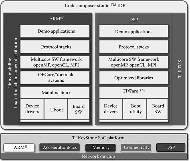
FIGURE 8.11 Keystone software platform from Texas Instruments. (From Texas Instruments Appnote. www.ti.com/lit/pdf/spry231.)
Power-efficient CMOS processes integrate hardware techniques that enable granularly defined low-power modes, and voltage and frequency scaling. Software APIs make these techniques readily available to the application for control through the RTOS, and test tools help the designer evaluate different implementations for power consumption. This enables such fine-grained control of low-power modes and voltage/frequency scaling on a per core granularity. Software is designed to use the DSP’s internal memory wherever possible, keeping high-bandwidth memory on-chip and reserving external memory for low-speed, occasional access. Off-chip memory also serves well for booting, and can be powered down after startup. Software is typically optimized for performance to reduce the code’s footprint in memory and the number of instruction fetches. Tighter code makes better use of the cache and internal instruction buffers. As it generally runs faster, it reduces the system’s time in active mode.
8.8 Conclusion
On-chip power-optimization techniques in multicore platforms now offer more granular control, more power-saving modes, and more complete information about processor power consumption than ever before. Further, the DSP development tools give designers more insight into how the systems consume power and provide techniques for lowering power consumption via on-chip hardware. Algorithms need to be developed taking the underlying architecture into consideration. Software needs to be aware of the power and energy management opportunities in the underlying hardware and maximize the energy savings. To continue to improve on the quest for efficient signal processing, a holistic approach taking into consideration algorithms, underlying architecture, and the systems is required.
References
1. Koomey, J. The Computing Trend that Will Change Everything. MIT Technology Review, 2012. http://www.technologyreview.com/news/427444/the-computing-trend-that-will-change-everything/.
2. Karam, L. J., I. AlKamal, A. Gatherer, G. A. Frantz, D. V. Anderson, and B. L. Evans. Trends in multi-core DSP platforms. Signal Processing Magazine, IEEE 26(6): 38–49, 2009.
3. Strass, W. Forward Concepts. eNewsletter, Oct. 2013. https://fwdconcepts.com/enewsletter-101613/.
4. Visconti, F. The Role of Digital Signal Processors (DSP) for 3G Mobile Communication Systems, Engineering Universe For Scientific Research And Management (EUSRM), 1(5), 2009.
5. Mick, J. Samsung Unleashes 28 nm Octacore Chip for Smartphones, Tablets, DailyTech, accessed August 2013, http://www.dailytech.com/Samsung+Unleashes+28+nm+Octacore+Chip+for+Smartphones+Tablets/article32023.htm.
6. Arthur, C. Tablet shipments suggest a crossing point with PCs might not be far off, The Guardian, accessed August 2013, http://www.theguardian.com/technology/2013/feb/01/tablets-crossing-point-pcs.
7. Woo, S. Samsung Analyst Day 2013, The Semiconductor Wiki Project, accessed August 2013, http://www.semiwiki.com/forum/files/S.LSI_Namsung%20Woo_Samsung%20System%20LSI%20Business-1.pdf.
8. ASCI Red, Wikipedia, accessed August 2013, http://en.wikipedia.org/wiki/ASCI_Red.
9. FLOPS, Wikipedia, accessed August 2013, http://en.wikipedia.org/wiki/FLOPS.
10. TOP500, Wikipedia, accessed August 2013, http://en.wikipedia.org/wiki/TOP500.
11. Texas Instruments Appnote SPRT619. TMS320C66x multicore DSPs for high-performance computing, accessed August 2013, http://www.ti.com/dsp/docs/dspsplashtsp?contentId=145760.
12. DARPA PERFECT program. http://www.darpa.mil/Our_Work/MTO/Programs/Power_Efficiency_Revolution_for_Embedded_Computing_Technologies_(PERFECT).aspx.
13. General-purpose computing on graphics processing units, Wikipedia, accessed August 2013, http://en.wikipedia.org/wiki/General-purpose_computing_on_graphics_processing_units.
14. Damodaran, R. et al. A 1.25 GHz 0.8 W C66x DSP Core in 40nm CMOS. 25th International Conference on VLSI Design (VLSID), IEEE, pp. 286–291. Hyderabad, India, 2012.
15. Friedmann, A. TI’s new TMS320C66x fixed- and floating-point DSP core conquers the “Need for Speed,” Texas Instruments Whitepaper SPRY147, accessed August 2013, http://www.ti.com/lit/wp/spry147/spry147.pdf.
16. Frantz, G. Digital signal processor trends, IEEE Micro, 20(6), 52–59, 2000.
17. Williams, J. et al. Computational Density of Fixed and Reconfigurable Multi-Core Devices for Application Acceleration, 2008. http://rssi.ncsa.illinois.edu/proceedings/academic/Williams.pdf.
18. Saban, N. Multicore DSP vs. GPUs, Workshop on GPU & Parallel Computing, Israel, January 2011, http://www.sagivtech.com/contentManagment/uploadedFiles/fileGallery/Multi_core_DSPs_vs_GPUs_TI_for_distribution.pdf.
19. Lucent Technologies. A New Measure of DSP. Allentown, PA, 1997.
20. Berkeley Design Technology, Inc., accessed August 2013, http://www.bdti.com.
21. The Embedded Microprocessor Benchmark Consortium (EEMBC), accessed August 2013, http://www.eembc.org.
22. Hybrid Memory Cube Consortium, accessed August 2013, http://www.hybridmemorycube.org.
23. JESD235 Open Standard Specifications, JEDEC Solid State Technology Association, October 2013, http://www.jedec.org/standards-documents/docs/jesd235.
24. National Instruments whitepaper. PXI Express Specification Tutorial, 2010, http://www.ni.com/white-paper/2876/en/.
25. Kollig, P., C. Osborne, and T. Henriksson. Heterogeneous multi-core platform for consumer multimedia applications. Design, Automation & Test in Europe Conference & Exhibition (DATE), IEEE, Nice, France, pp. 1254–1259, 2009.
26. Tan, E. J. and B. H. Wendi. DSP architectures: Past, present and futures. ACM SIGARCH Computer Architecture News, 31(3): 6–19, 2003.
27. Oshana, R. DSP for Embedded and Real-Time Systems. Newnes: Boston, MA, 2012.
28. Texas Instruments Keystone Platform. http://www.ti.com/lsds/ti/dsp/keystone_arm/overview.page.
29. CEVA-XC Family. http://www.ceva-dsp.com/CEVA-XC-Family.
30. Freescale QorIQ Qonverge Platform, 2013. http://www.freescale.com/webapp/sps/site/overview.jsp?code=QORIQ_QONVERGE.
31. Texas Instruments Appnote. Accelerate multicore application development with KeyStone software. www.ti.com/lit/pdf/spry231.