
17 Dynamic Intrinsic Chip ID for Hardware Security
Toshiaki Kirihata and Sami Rosenblatt
Contents
17.3 High-Performance Embedded–Dynamic Random Access Memory
17.4 Retention-Based Intrinsic Chip ID
17.5 Dynamic Intrinsic Chip ID
17.6 Dynamic Intrinsic Chip ID Hardware Authentication
17.7 Field-Tolerant Intrinsic Chip ID
17.8 Field-Tolerant Hardware Authentication
17.9 Security and Authentication Enhancement for Intrinsic Chip ID
17.1 Introduction
Rapid progress in science and technology has brought great convenience for business and personal life alike. In particular, evolutionary advancements in nanoscale semiconductor technology [1], while improving performance, are key contributors to the miniaturization of electronic products. These improvements, in turn, have introduced consumers to personal computing and the information era. Lately, consumer products for mobile computing and communication have been the fastest growing segments to drive the semiconductor industry. These new products further incorporate wireless, Internet, and revolutionary social network applications, allowing interpersonal communication without restrictions of time and place. However, these new products and services have created various privacy and security concerns. Although communicating with people whom one has never met is already common in a person’s virtual life, it may result in a breach of privacy as well as in virus attacks to the personal system. Therefore, developing high-security products and services is an urgent task not only for business, but also for the semiconductor industry.
Security and privacy in the digital network use cryptographic protocols [2] with open and private keys, which are now commonplace in the industry. However, this high level of security cannot be realized without establishing a root of trust, which includes the use of highly reliable hardware. Thus, hardware security [3] is an equally, if not more, important concern for high-security systems. Hardware security requires identification, authentication, encryption, and decryption engines [4]. Unfortunately, a recent surge in counterfeit hardware has resulted in the occasional distribution of cheap, fake chips in the industry [5]. Distribution of these counterfeit chips not only leads to reduced product reliability, but also further increases privacy and security risks. These counterfeits are typically the result of either discarded chips reintroduced into the supply chain, or of fabrication of cheap copies that pass as authentic, reducing cost without significant security. Systems using unauthentic chips are consequently exposed to a high risk of failure in the field. More importantly, using fake chips for banking or defense systems results in a potentially unacceptable risk for national security. Thus, the reliability of the task of identifying hardware has become a necessity in contemporary security, which in turn requires a method for highly reliable chip identification and authentication using semiconductor components.
Figure 17.1 summarizes the hardware identification method. The simplest approach uses an identifier (ID) such as text that is uniquely assigned to each hardware unit. However, as the ID can be read by anyone, a counterfeit part can be created by simply writing the ID on the fake hardware. This approach is, therefore, not secure at all. Recent hardware, in particular a very-large-scale integration (VLSI) chip, uses embedded fuses for IDs that are uniquely assigned and programmed in each of the VLSI chips. This fuse approach is somewhat secure, because the ID cannot be read without breaking the module, whereas a special tool is necessary for writing the ID to the fuses. Older fuse technology uses laser [6] for blowing the fuses, which is a large and expensive process. The evolution of fuse technology has resulted in the electrically blowable fuse approach (eFUSE) [7]. This makes it possible to create a high-density one-time programmable read-only memory (OTPROM) [8,9] that can be used for chip ID, as well as for other programming elements such as redundancy replacement. Regardless of laser fuse or OTPROM using eFUSE, the fuses are visible by optical or electronic microscopy, and therefore the programmed ID information can still be obtained after delayering. Using nonvolatile memory such as embedded flash memory [10,11] makes it difficult to obtain the ID by the delayering method; however, direct readout from the chip is still possible if the read method is known.
There are two fundamental problems with the existing ID approaches. First, all of them use an ID that is extrinsic to the hardware. These extrinsic IDs are not integral to the hardware, as the information needs to be written or programmed, and they can be subsequently read by some method. Second, the ID can be cloned as long as it is known. These weaknesses make it possible to create counterfeits by emulating the ID in multiple fake chips. Therefore, the challenges to creating secure IDs are to make it difficult for unauthorized people to detect the ID and to make it impossible, if not impractical, to create a clone of the ID even if it can be made known with reasonable effort. An intrinsic chip ID uses intrinsic VLSI features, constituting an ideal solution for high-security applications and making it prohibitive to make fake copies.
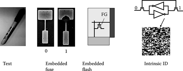
FIGURE 17.1 Evolution of chip identification (ID).
In this chapter, we discuss an intrinsic chip ID using bitmaps of an embedded dynamic random-access memory (eDRAM) macro. Section 17.2 introduces the concept of intrinsic ID, followed by a review of the existing approaches. In Section 17.3, principles of eDRAM are discussed. Sections 17.4 through 17.6 are concerned with the dynamic intrinsic ID approach using retention signatures of a one-transistor and one-capacitor cell. In Sections 17.7 and 17.8, a field-tolerant method is explored, which improves success of intrinsic ID authentication in a field. Section 17.9 introduces a security and authentication enhancement method using a multi-ID approach. Section 17.10 summarizes the chapter and briefly discusses the future challenges for intrinsic ID research and development.
17.2 Intrinsic Chip ID
Fingerprints are widely used for secure identification of individuals. A human fingerprint is a unique and unclonable feature that each person possesses. In a similar fashion, a secure intrinsic ID exploits intrinsic features of a VLSI chip. Such features arise from random process variations, and can be used to generate an ID that cannot be reverse-engineered or easily emulated, also called a “Physically Unclonable Function (PUF)” [12–37]. This thus greatly improves chip security over the existing extrinsic ID approach. In this section, we discuss the intrinsic ID generation and authentication concept using random process variations in manufacturing, and their challenges.
An intrinsic chip ID converts process variations in manufacturing into a digital binary vector for chip identification. Figure 17.2 shows intrinsic ID generation methods using complementary metal–oxide–semiconductor (CMOS) cross-coupled inverters. In the simplest approach (a), each of the inverters drives the other’s output, nodes A and B, respectively. This structure is commonly used as a temporary storage element or as a bus keeper [14] for VLSI design, and constitutes an ideal element for intrinsic ID. When used in ID generation, the cross-coupled inverter is powered up without node initialization. This power-up method, accomplished by raising a main power supply voltage (VDD), naturally determines the states of A and B as a consequence of the p-type metal-oxide-semiconductor (PMOS) and n-type metal-oxide-semiconductor (NMOS) threshold mismatch of the cross-coupled inverters. The A and B states after power-up can be used as a bit of an intrinsic ID. These states, however, may not be stable, as they may be sensitive to noise during power-up. Therefore, a preferred approach (b) includes two additional access transistors that force nodes A and B to ground (GND) level as soon as power is turned on. The states can, therefore, be determined by the PMOS threshold mismatch of the cross-coupled inverters, as nodes A and B are forced to GND level until one of the PMOS is strongly turned on, eliminating instability resulting from power-up noise. This approach (b) has two advantages. First, the threshold voltage (VT) mismatch of the cross-coupled inverters depends on the local PMOS VT mismatch, and can potentially minimize the systematic impacts of lithography, temperature, or noise. Second, this structure is identical to that of the six-transistor static random access memory (SRAM) cell, and as such enables the use of SRAM arrays and their bitmap [15–23] for intrinsic ID generation. The end result is a significant increase of density with the added benefit of allowing a product memory array to be used for intrinsic ID generation.
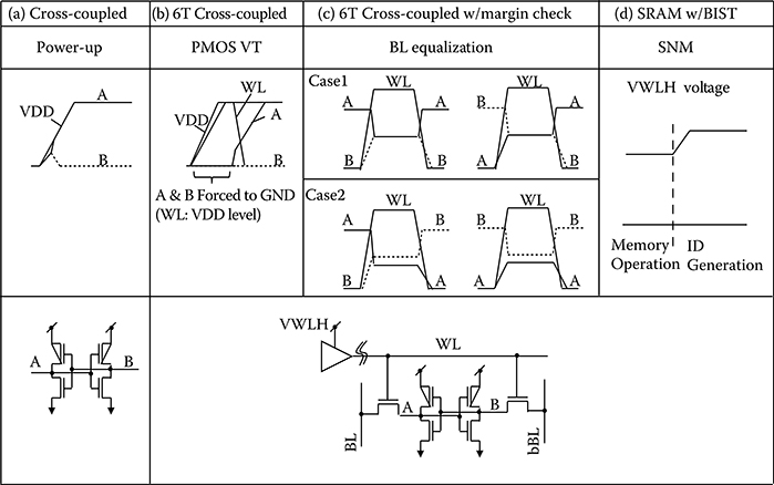
FIGURE 17.2 Physically unclonable fuse (PUF) using cross-coupled inverter. (a) Cross-coupled inverter approach. The states of A and B are naturally determined after power-up. (b) 6 Transistor (6T) SRAM cell approach. The nodes A and B are forced to GND level until one of the PMOS is strongly turned on, eliminating instability due to power-up noise. (c) 6T SRAM cell approach with margin check. Nodes A and B are equalized from the predetermined 0 and 1 states, and they generate the random bit pattern by deactivating the wordline (WL). (d) Static-noise margin (SNM) approach. The fail bits are generated by reducing SNM. The bit pattern is preferably generated using a built-in-self-test (BIST) engine.
Approach (b) may be improved by using an ID margin detection method to eliminate unstable bits. Unlike the power-up intrinsic ID generation, approach (c) [22] generates the ID after completing a power-up sequence similar to that of conventional memory operation. Before ID generation, the A and B nodes are initially set to predetermined states (“1” and “0,” or “0” and “1”). This initialization is realized by means of a SRAM write mode. Writing “1” sets nodes A and B to “1” and “0,” and writing “0” sets nodes A and B at “0” and “1,” respectively. Activation of the wordline (WL) opens the access transistor, whereas the bitlines (BLs) of the pair are held at GND level. This results in a short-circuit of nodes A and B, and the BL and bBL equalization levels are determined by intrinsic features such as threshold voltage mismatch or transistor strength of the cell. Cells containing balanced cross-coupled inverters allow nodes A and B to be equalized, and result in a small voltage difference between BL pairs during equalization, as shown in case 1. On the other hand, cells having largely imbalanced cross-coupled inverters remain unequalized, or flip the states in a preferred direction, as shown in case 2.
Evaluation or generation of the intrinsic ID is enabled by deactivation of the WL, which in turn disables the equalization of nodes A and B. This results in determining the node A and B states naturally. For the well-equalized BL cell (case 1), a generated bit is likely unstable. Otherwise, the generated bit is determined by the initial predetermined voltages of the nodes. On the other hand, a bit generated from the cell that is not well equalized (case 2) is always stable regardless of the initial predetermined voltages of the nodes. Generation and evaluation must be performed using both initial node states (A and B at “0” and “1” and “1” and “0”) to assess the intrinsic stability of the bit.
On-chip intrinsic ID generation requires a built-in-self-test (BIST) engine [38]. Fortunately, the on-chip memory in a logic chip is typically supported by BIST, and therefore is readily available for intrinsic ID generation without additional overhead. The fourth approach (d) uses a BIST engine in the generation of a random binary vector derived from checking the static-noise margin (SNM) of a SRAM array [23]. For memory operation, the wordline high voltage (VWLH) is adjusted to have a sufficient SNM when the WL goes high. For ID generation, the VWLH voltage is increased to reduce the SNM. This results in a fail for a weak cell when the WL goes high. To weed out the weakest bits, this approach includes a feedback loop between the number of fails and the VWLH voltage supply. This feedback remains active until the fail count (FC) reasonably matches a predetermined number. The result is the generation of a stable random bit pattern comprised of the fail bit addresses, which are detected and recorded using the on-chip BIST.
An intrinsic chip ID can be further implemented using a delay-based PUF. Ring-oscillator (RO)–based PUFs [24,25] compare the delay between ROs while generating unclonable random bit strings. Similar to the RO PUF, an arbiter-based PUF [26] is composed of delay paths for signals A and B and an arbiter located at the end of the delay path. The arbiter outputs “1” when signal A arrives earlier than B, otherwise it outputs “0.” Because the delay path is determined by intrinsic features in manufacturing, the output bit can be random. The challenge of this approach is to lay out the signal path symmetrically to minimize the normal delay difference between the two paths. Otherwise, the output will be skewed. Another approach [27] detects an analog voltage determined by the threshold of the MOS transistors, which is subsequently converted to a binary identification sequence using an auto-zeroing comparator. The one-time oxide breakdown PUF [28] leverages the fact that a stress condition such as high voltage can break weak cells with a higher confidence than strong cells, resulting in permanent random intrinsic ID generation. The concern with this permanent approach is that the ID bits can be detected by delayering the chip in a manner similar to the extrinsic fuse approach. Bit-string generation based on resistance variation in metals and transistors has also been reported [29].
The ultimate intrinsic ID is a fingerprint derived from product intrinsic features without need for allocating additional silicon for chip identification. VLSI chips, in particular recent multicore and multithread microprocessers [39,40], include tens or hundreds of on-chip cache memories. Using the on-chip cache as a fingerprint intrinsic ID may therefore offer an ideal solution for highly secure identification, because the memory can be used for the generation of enormous intrinsic IDs without requiring additional expensive silicon from a high-performance system. The challenges for this application reside in providing the intrinsic ID function without degrading the product chip features.
In this chapter, we discuss intrinsic chip ID generation and authentication using 32 nm HiK/metal gate eDRAM product developed for next generation multicore and multithread microprocessor. The next section describes the principle of eDRAM macro operation and the retention signature, which will be used for intrinsic ID generation and authentication to be discussed in following sections.
17.3 High-Performance Embedded–Dynamic Random Access Memory
For nanometer technology, it is desirable and essential to integrate more functions within a single die. DRAM integration with a high-performance logic process (eDRAM) [38] not only reduces packaging cost, but it also significantly increases the memory bandwidth while eliminating input and output (I/O) electrical communication that is noisy and power hungry. Because of the smaller memory cell size, the eDRAM can be approximately 3–6 times denser than embedded-SRAM, and operates with low-power dissipation and 1000 × better soft-error rate. eDRAM macros [41] that are based on high-performance logic are extremely vital microelectronic components, making it possible to integrate 32-MB on-chip cache memory on POWER7TM processors [39].
eDRAM employs a one-transistor and one capacitor (1T1C) as a memory cell that stores a data bit for a read and write operation. To reduce the cell size, the capacitor is built using either stack [42] or trench capacitor [43] structures. A deep trench capacitor approach is the preferred structure for eDRAM because the capacitor is built before device fabrication. This facilitates the implementation of a process fully compatible with logic technology, as transistor performance does not degrade because of capacitor fabrication, and design rules for back-end-of-lines (or metal wiring) remain the same as that of the logic technology. This results in an ideal technology solution for DRAM integration on a high-performance logic chip.
Figure 17.3 shows the overview of the eDRAM macro [41] for the POWER7 microprocessor [39]. The macro consists of four 292-Kb memory arrays stacked in the Y-direction, resulting in a density of 1.168 MB. These arrays are controlled by a peripheral circuit block (IOBLOCK) arranged at the bottom of the macro. The peripheral circuit block, in turn, consists of command and address receivers, decoders, and macro I/O circuitries used to control the memory arrays with given input commands.
Each 292-Kb memory array consists of 1T1C cells arranged in a two-dimensional matrix. The memory cells in the array including row and column redundancies are accessed by 264 WLs and 1200 BLs for row and column, respectively. The architecture is optimized for a L3 cache application while taking into account the performance, power, and I/O requirements. Unlike in conventional memory, the wordline drivers are placed in the area adjacent to the global sense amplifiers (GSAs), which are in turn controlled by the global WL drivers located in the peripheral circuit block (IOBLOCK). This orthogonally segmented WL architecture [38] is the key to realize the wide I/O organization.
The 292-Kb array is organized using eight 36.5-Kb microarrays for transistor microsense amplifier architecture [41]. A total of 32 cells with an additional redundant cell (total 33 cells) are coupled to the local bitline (LBL), and read or written using a local microsense amplifier (μSA). Eight groups of LBLs, each one with a μSA arranged in the same column, are coupled to a GSA through the global read and write BLs (RBL and WBL). This hierarchical approach is important both to improve performance and to reduce power dissipation for a 500-MHz random cycle.
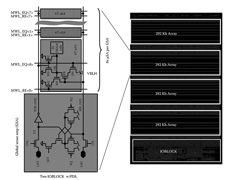
FIGURE 17.3 High-performance embedded–dynamic random access memory (eDRAM). (J. Barth, D. Plass, E. Nelson, C. Hwang, G. Fredeman, M. Sperling, A. Mathews et al., A 45 nm SOI embedded DRAM macros for POWER7TM processor 32-MByte on-chip L3 cache, IEEE Journal of Solid-State Circuits, 46[1], © 2011 IEEE.)
While in the stand-by state, the WL is held at a wordline low voltage (VWL), a negative voltage. This is key to turning all access transistors sufficiently off. Otherwise, the threshold of the access transistors must be increased, resulting in a higher WL boost voltage (VPP) requirement to turn the devices on. Signals MWL_EQs and MWL_REs are, respectively, high and low, to turn the LBL precharge device (PC) on, the NMOS foot device off, and the PMOS head device (PH) off. This signal configuration precharges all LBLs to the low level (GND), while disabling the NMOS read head device (RH) and the PMOS feedback device (FB). RBL and WBL are held high and low, respectively. When the 36.5-Kb microarray is selected for WL activation, the signal MWL_EQ goes low. This disables the NMOS (PC), floating the LBL in the selected subarray. The MWL_EQ signal in other unselected arrays remains at high level, keeping the precharge device of the unselected LBLs at low level. The low-going MWL_EQ also turns on the PMOS PH, enabling the PMOS feedback device. For writing 1 to the cell, RBL goes low. This allows the LBL to go high, resulting in a high voltage written to the corresponding capacitor. For writing 0 to the cell, WBL goes high. This keeps the LBL at the low level, resulting in a low voltage written to the corresponding capacitor.
When a read command is accepted, read data are transferred from the cell to the BL when the WL goes high. For reading 1 data, LBL goes high, which turns the NMOS RH on. This results in making RBL low when the signal MWL_RE goes high and the NMOS footer device (NF) turns on. At the same time, low-going RBL turns on the PMOS FB. This results in making the LBL go high. The high voltage on the LBL is written back to the corresponding cell. For reading 0 data, LBL stays at the low level, and the NMOS RH device remains disabled. RBL therefore stays at the high level. The RBL data are subsequently multiplexed by a column select signal (CSL) and communicated to the peripheral circuit block (IOBLOCK) through a local data bus pair (LDC and LDT) and then the primary data line (PDL) for data transfer. At the same time, the GSA senses the RBL in the high state, making WBL go high. This makes the write 0 device (W0) to turn on, forcing the LBL to the low level. Therefore, the low-level voltage on LBL is written back to the corresponding cell.
Precharge operation starts when the WL falls to the VWL voltage (negative voltage). MWL_EQ and MWL_RE go high and low, respectively, precharging the LBL to the low level. This concludes one 500-MHz random access memory cycle for < 1.5 nanoseconds latency.
After the deactivation of the WL, the data bits are kept inside the capacitors. However, the charge stored in them leaks as time goes on, and therefore they should be periodically read and written back. This is a unique but important requirement for DRAMs, and is known as the refresh operation. As long as the refresh is executed before the voltage of the storage nodes drops below the detection threshold of the SA, the data bits are maintained. The time interval during which a cell can hold the data bit is called retention time. The eDRAM intrinsic chip ID uses this retention signature in order to generate unclonable random bit patterns.
17.4 Retention-Based Intrinsic Chip ID
Figure 17.4 shows the concepts of intrinsic chip ID generation and authentication using retention signatures from eDRAM. Before ID generation, a logic 1 is written to all bit cells in an array, stored in the form of charge in the capacitors. However, the charge in each cell leaks as a function of time. Therefore, after waiting for a predetermined amount of time, the read data bits from the corresponding array may remain as 1 or change to 0. Preferably, the read operation may be managed by a BIST engine or, if not implemented, by an external tester. If the charge remains sufficiently high, the output (DQ) from the SA results in the expected value of 1, resulting in a PASS. If the charge leaks beyond the SA detection point of 1, then DQ is 0, resulting in a FAIL. Because each cell has a different retention time, the PASS and FAIL address locations in the array are random and physically unclonable. The array bit pattern (BITMAP) may then be recorded as the intrinsic chip ID in a bit-string format such that the length of the string is equal to the array size, and where a passing bit (pbit) is stored as 0, and a failing bit (fbit) is stored as 1, ordered from the first to last logical addresses. Notice that the bits of interest for the intrinsic ID binary string are the fbits, and therefore their binary values are conveniently set to 1 as opposed to their logical 0 values after the read operation.
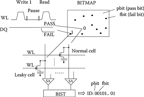
FIGURE 17.4 Retention-based intrinsic chip ID.
Because generation of fbits can be done by changing the predetermined pause time in a nondestructive manner, this retention-based intrinsic ID approach allows for use of the eDRAM array IP as is. However, the retention time depends significantly on various process or design parameters, including subthreshold leakage, junction leakage, GIDL, bitline capacitance, cell capacitance, and noise. Therefore, chip authentication using retention time becomes highly sensitive to the precise test condition used during ID generation. In addition, creating fbits at low temperatures requires a long pause time, increasing the time for ID generation.
To improve bit stability, retention-based ID generation uses a higher VWL than the product target voltage. This is equivalent to emulating a low-threshold access transistor, forcing the retention signature to be sub-threshold driven. Figure 17.5 employs a VWL controlled by the VWL generator (VWLG) [44] using a feedback loop driven by the array’s FC. Using higher VWL voltage increases the subthreshold leakage of the access transistor, which in turn generates more fbits in the bitmap. This VWL voltage can therefore be used as a tunable array input parameter controlling the number of fbits in the BITMAP.
Specifically for applications, product use is optimized using a negative VWL resulting in no retention failures within a predetermined retention target. This is labeled Memory mode in Figure 17.5. In the ID mode, significantly higher VWL voltage is applied to the array such that the retention time is determined by sub-threshold leakage. To reduce the dependency on temperature and voltage conditions during ID generation, the retention-based intrinsic ID approach includes a counter for the number of fbits in the BITMAP. VWLG adjusts the VWL voltage such that the number of fbits matches the predetermined target number. Consequently, implementing feedback between the BIST-counter pair and VWLG enables the generation of an intrinsic BITMAP (or binary string) for any target FC of the retention failures (or 1 in bit string). The target FC may be given by the Original Equipment Manufacturer (OEM) as a CHALLENGE to the chip. The generated intrinsic ID vector with the given FC is recorded in the OEM database to identify the chip for subsequent authentication.
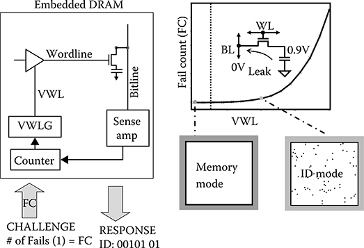
FIGURE 17.5 Method to generate the bitmap with wordline low voltage (VWL) control. Fail count (FC) is used as a CHALLENGE. VWL voltage is controlled by the VWL generator (VWLG) or an external tester such that the FC in the bitmap satisfies the target FC. The RESPONSE is the bit string created by the bitmap, where 0 and 1 are PASS and FAIL address locations in the array, respectively. (Rosenblatt, S. et al., Field tolerant dynamic intrinsic chip ID using 32 nm high-K/metal gate SOI embedded DRAM, IEEE J.Solid-StateCircuits, 48[4], © 2013 IEEE.)
Authentication is realized by extracting the ID string from the intrinsic ID binary vector using the same target FC as used earlier during the recording phase. Once the bit string with the target FC is achieved, the chip outputs the generated ID bit string as a RESPONSE to the OEM, and the database searches for the ID from within its list until it identifies the corresponding chip.
The uniqueness of a set of IDs for a given number of parts can be calculated exactly. The probability of generating n different IDs by randomly choosing j fbits out of an array of size i is given by the following expression (see Table 17.1):
For practical implementations, the inherent information entropy contained in an ID set is already very large. For example, a set of 4 Kb strings containing 100 fbits, each will be unique up to roughly 10100 parts.
17.5 Dynamic Intrinsic Chip ID
The retention-based intrinsic chip ID allows for control of the number of fails in the array bit pattern (BITMAP) by means of the VWL. During generation, the number of the fails (fbits) in the ID matches a target number, and therefore that number can be adjusted by the VWL voltage. It is not practical, however, to generate the same exact number of fails as set by the target, and even if it were, it would be too expensive or time consuming. In addition, it may not be safer from a security standpoint to use the exact same ID binary string for each authentication request. The dynamic intrinsic ID approach is introduced to eliminate the necessity to generate the exact same FC while enhancing ID security.
Table 17.1 Probability of Creating n Unique Intrinsic IDs with j Fails in Array of Size i
ID Generation Turn |
1 |
2 |
— |
n |
Failing bit addresses in IDGEN |
F1 = {f11, f12, f1j |
F2 = {f21, f22, f2j |
— |
Fn = {fn1, fn2, fnj |
# Combinations available per turn resulting in a new IDGEN |
— |
|||
# Total combinations per IDGEN per turn |
— |
|||
Probability of choosing a new IDGEN per turn |
— |
|||
Joint probability PBASE = P1 × P2…×Pn |
|
|
|
Figure 17.6 shows the concept of dynamic chip ID generation and authentication. It consists of a window-based authentication method using retention time in which the fbit locations corresponding to an ID with a larger FC number include the fbit locations corresponding to an ID with a smaller number. Unlike the direct intrinsic ID method of Section 17.4, the dynamic intrinsic ID method uses a pair of IDs (IDMIN and IDMAX). IDMIN is the intrinsic ID binary string corresponding to a target minimum FC, FCMIN (i.e., 10). IDMAX is the intrinsic ID binary string corresponding to a target maximum FC, FCMAX (i.e., 100). During ID generation, the IDMIN and IDMAX pair is generated by adjusting the VWL voltage while counting the fails until the respective FCMIN and FCMAX targets are achieved. These FC targets are used to determine the target window (i.e., 10–100) for subsequent authentication. Because of the nature of the DRAM cell, the fbits in the IDMAX bit string include those in the IDMIN bit string (Generation Rule).
Authentication uses the FC target FCAUTH inside the target window, such that FCMIN ≤ FCAUTH ≤ FCMAX. The FCAUTH target is dynamically changed within the window at each authentication request (i.e., 30, then 50, then 70), significantly improving hardware security. By construction, IDAUTH, the regenerated intrinsic ID corresponding to FCAUTH, should have a FC at least larger than IDMIN and at most smaller than IDMAX. Again because of the nature of the DRAM cell, the fbits in IDAUTH (i.e., 0010011001100101) obtained from the FCAUTH target (i.e., 50) include those in IDMIN (i.e., 0010000001100001) obtained from the FCMIN target (i.e., 10), and are included in the fbits in IDMAX (i.e., 0010111001100101) obtained from the FCMAX target (i.e., 100). Authentication using IDAUTH is therefore possible as long as the generated FC is within the target window defined by the pair IDMIN and IDMAX (Authentication Rule).
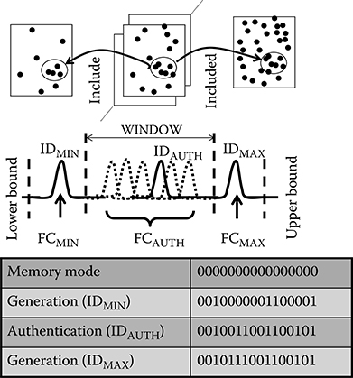
FIGURE 17.6 Concept of dynamic chip ID generation and authentication method.
As ID generation does not need to satisfy the exact FC target provided by the CHALLENGE, window-based authentication simplifies ID generation. As shown in Figure 17.6, the FC in typical hardware has a distribution centered about the target FC. It is therefore important to determine a target window suitable for authentication while considering the FC distribution, to not violate the authentication rule. One possible violation of the rule can happen if too few fails or too many fails in the ID pair reduces the uniqueness of the chip ID. Hence, it is necessary to establish a lower bound for FCMIN and an upper bound for FCMAX of the generated ID pair to avoid false positive authentication (misidentification of the ID with others), which can be regarded as a Window Rule. As an example of what can happen without boundaries, it is possible to authenticate 0 fails or 100% fails for any chip, which is not an acceptable situation. The number of fails in the ID should therefore be within a predetermined window to satisfy ID uniqueness for the target application while remaining guaranteed with an analytically chosen degree of confidence.
Figure 17.7 exemplifies the chip- and system-level architecture enabling the dynamic intrinsic ID method. For ID generation, the OEM server sends the ID generation request (CHALLENGE) with the target FC pair (FCMIN and FCMAX). This pair is used one time as a CHALLENGE for generating the corresponding chip IDMIN and IDMAX pair. On receiving the CHALLENGE, the chip starts testing the first 4-Kb memory segment (f) with the BIST. The test first verifies if the segment (SEG) is reliable for product use, such that the product’s nominal VWL voltage produces no fails. To avoid process edge effects, the edge segments are not used. If the BIST detects a fail, the segment is not reliable. The circuit SEG then increments the segment number to choose the next segment (g) and the BIST tests it next. After confirming no fails in the selected segment, the BIST requests the VWL generator to increase the VWL voltage. This emulates reducing the threshold of the access transistor, resulting in a shorter retention time. The BIST retests the selected segment with the new increased VWL voltage, and checks if the FC is within the FCMIN band (FCMIN +/− GB), where GB is the predetermined guard band. The BIST test continues until the BIST has found the first bitmap having FC satisfying the FCMIN band by incrementing the VWL voltage. The BIST test then starts searching for the second bitmap using an FC target satisfying the FCMAX window while incrementing the VWL voltage. The ID generator circuit (IDGEN) reformats the detected first and second bitmaps to the two binary bit strings composed of PASS and FAIL bits as 0 and 1 bits, respectively. This is the pair IDMIN and IDMAX. The chip then confirms if the locations of fbits in IDMAX include all fbits in the IDMIN.
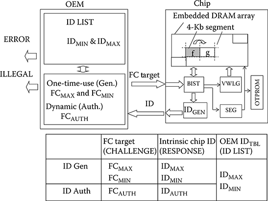
FIGURE 17.7 Chip and system architecture for dynamic chip ID.
If the IDMIN and IDMAX pair does not satisfy the Generation Rule, the circuit SEG chooses a new segment, and starts testing the new one to search for a new ID pair. The confirmed IDMIN and IDMAX pair is then sent to the system. The system first checks if the pair is unique (no collisions with other pairs). If the pair passes the uniqueness test, the system stores the ID pair in its list for subsequent authentication. The segment (i.e., g) used for ID generation is then stored in OTPROM within the chip for later authentication. If the pair fails the uniqueness test, the system requests new ID generation to search for a new ID pair using a new segment. In case no ID pair is found among all segments, the system outputs the error code (ERROR), resulting in a discarded chip.
The ID authentication request is enabled when the authentication CHALLENGE FCAUTH is provided to the chip. The chip searches for the bitmap having FC satisfying the FCAUTH band by incrementing the VWL voltage in a manner similar to the ID generation process, after confirming there are no fails with nominal VWL voltage (product specifications). The detected bitmap is reformatted to the IDAUTH binary bit string. This string is then output to the system.
The system checks if the FC of IDAUTH is the same as the given CHALLENGE (FCAUTH). If these FCs do not match within a specified tolerance (FCAUTH +/− GB), the chip may be counterfeit and spoofing a known chip ID. The dynamic intrinsic chip ID, therefore, protects against illegal use with output code ILLEGAL. This prevents against a counterfeiter using a previous CHALLENGE by preprogramming it. If the FC is valid, the system searches within its list (ID LIST) for the chip having an IDMIN and IDMAX pair whose fbit locations are included in and include IDAUTH, respectively (in other words, satisfies the Authentication Rule).
The uniqueness of an authentication key IDAUTH in recognizing a valid chip is minimized when IDAUTH = IDMIN. After all, an authentication key with FCAUTH = FCMIN has the least number of combinations to choose from and is by construction the least unique. It follows that authentication of a pair of IDMIN and IDMAX using the IDMIN bit string has the lowest uniqueness rating for dynamic authentication. For n parts, with a binary string of i bits, FCMIN = k and FCMAX = j, an approximate analytical expression that provides a lower bound for the uniqueness of the pair of IDs is given by the following expression (see Table 17.2):
As seen in Figure 17.8, the analytical model shows > 99.999% ID uniqueness using a 4-Kb segment (i = 4096), lower bound of 12 (k = 12 or FCMIN = 12), and upper bound of 128 (j = 128 or FCMAX = 128) for 106 parts (n = 106). The actual uniqueness is characterized by the probability PUNIQUE, which is typically larger than PMIN. They are equal only when all the IDMAX in the set have no fails in common. Figure 17.9 compares the accuracy of the analytical expressions in Equation 17.2 with Monte Carlo simulations of the dynamic intrinsic ID method for various input parameters.
Table 17.2 ProbabilityPUNIQUE That Retention-Based Dynamic Intrinsic ID Set Is Unique. Number of Chips = n, Array Size = i, FCMAX Target = j, FCMIN Target = k
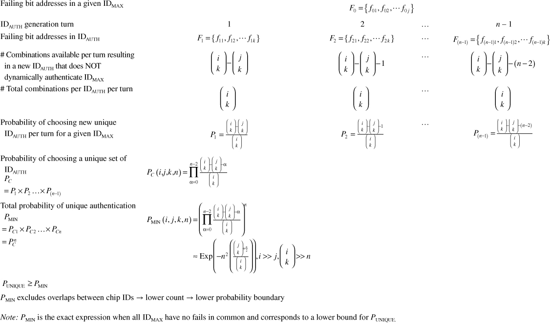
Note: PMIN is the exact expression when all IDMAX have no fails in common and corresponds to a lower bound for PUNIQUE.
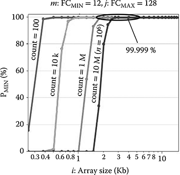
FIGURE 17.8 Calculated probability of ID uniqueness with Equation 17.2. (Rosenblatt, S. et al., Field tolerant dynamic intrinsic chip ID using 32 nm high-K/metal gate SOI embedded DRAM, IEEE J. Solid-State Circuits, 48[4], © 2013 IEEE.)
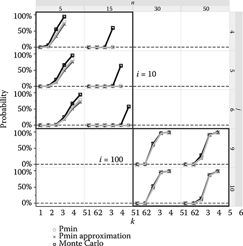
FIGURE 17.9 Probability of uniqueness of the retention-based dynamic intrinsic ID set using analytical expressions for PMIN (exact and approximate from Table 17.2), and Monte Carlo of this probability for 10,000 simulation sets. In the Monte Carlo, the k fails used for authentication are taken from the sample of n chips. Results are shown for i = 10 and 100. When j is much smaller than i, all the methods of estimating the probability converge toward each other, demonstrating the accuracy of the model.
17.6 Dynamic Intrinsic Chip ID Hardware Authentication
The concept of dynamic ID generation and authentication has been studied using 32 nm SOI eDRAM [45], which was a base design for an eDRAM macro IP for an IBM microprocessor [46]. Figure 17.10 shows a chip microphotograph of (a) an eDRAM array and (b) the test site of the IP used for this feasibility study along with its features. The eDRAM uses high-performance SOI eDRAM design features including 6T microsense amplifier and orthogonal WL architecture developed for POWER7 [41].
The IP used in this feasibility demonstration does include neither BIST engine nor a VWLG, and therefore the VWL voltage is controlled externally by the tester with a resolution of 5 mV. Before generating the ID, confirmation of no fails in the target 4-Kb segment is done using a nominal (within product specifications) VWL, also known as “Memory mode.” In this study, CHALLENGEs of FCMIN = 25 and FCMAX = 95 were used to generate a pair of intrinsic IDs. The eDRAM was tested repeatedly, varying the VWL in the tester to search for a binary string with fbit count close to, but not necessarily equal to, the desired target, as long as the Generation Rule was satisfied. If a pair of 4 Kb binary strings (IDMIN and IDMAX) was found which:
Reasonably matched the corresponding CHALLENGES: FCMIN = 25 and FCMAX = 95
Satisfied the Generation Rule: the fbit locations of IDMAX included the fbit locations of IDMIN
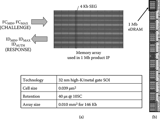
FIGURE 17.10 Chip microphotograph of (a) an eDRAM array and (b) the test site of the IP used for this feasibility study along with its features. (Rosenblatt, S. et al., Field tolerant dynamic intrinsic chip ID using 32 nm high-K/metal gate SOI embedded DRAM, IEEE J. Solid-State Circuits, 48[4], © 2013 IEEE.)
The ID pair was stored in an ID management system for authentication; else, the generation scheme was applied to successive 4 Kb SEGs of the array until a suitable area was found. Beginning with the “Memory mode” condition of no fails, the typical time to find the target number of fails required was 30 minutes per chip. The search time can be reduced significantly by means of a binary search [47].
For the purposes of authentication security and counterfeit prevention demonstration, chip authentication was realized by using different CHALLENGEs, selected as a different FC value at each authentication request, for example, a FCAUTH of 65 that is between FCMIN of 25 and FCMAX of 95. Similar to IDMIN and IDMAX pair generation, VWL was adjusted across multiple tests of the 4 Kb SEG manager circuit originally used for IDMIN and IDMAX pair generation. The voltage was adjusted until an IDAUTH binary string was generated with a number of fbits close to FCAUTH of 65. The IDAUTH string vector was the output of the system, and the string was compared to the list of IDMIN and IDMAX pairs previously stored in the system to identify the corresponding chip. A match occurred when the IDAUTH string included all of the fbit locations in IDMIN and was included in the fbit locations in IDMAX for a pair of strings in the database (Authentication Rule from Section 17.5). If the bit string IDAUTH did not follow the rule for any IDMIN and IDMAX pair in the list, then the chip was deemed invalid.
Figure 17.11a shows the measured ID distribution generated by CHALLENGEs (FCMIN = 25, FCMAX = 95, and FCAUTH = 65) for 346 chips at a fixed temperature of 25°C and voltage of VDD = 0.9 V. It was confirmed that the 346 chips can be uniquely identified by the dynamic retention-based chip ID generation and authentication rules. Detailed analysis of the data shows that the mean/standard deviation of overlapping fbit locations for (b) the Monte Carlo simulation and (c) hardware are 0.55/0.73 and 0.58/0.76, respectively, showing a good correlation between simulation and hardware results. Figures 17.12a and b show the fbit overlap count by chip of 32 IDs between generation and authentication for simulation and hardware, respectively. Each ID was generated with 100 fbits and regenerated with 50 fbits in 32 different chips. The results show an excellent agreement between hardware and simulation, demonstrating a maximum of 5 overlapping fbits in any one of the 32 × 32 combinations.
17.7 Field-Tolerant Intrinsic Chip ID
The dynamic intrinsic ID approach allows for some bit changes as long as the fbit addresses in IDAUTH are included in the IDMAX fbits. It may, however, result in an error if some newly generated fbits in IDAUTH violate the authentication rule. This may happen if all the fbits in IDMIN do not constitute any longer a subset of the fbits in IDAUTH, or if all of the newly generated fbits in IDAUTH cease to be a subset of the ones in IDMAX. This results in false-negative authentication. Therefore, it is necessary to exert precise voltage and temperature control, so that IDAUTH generation can emulate the conditions used for ID generation. This is impractical, if not very expensive, for use in the field. Even if the exact same conditions are used in the field, some unstable fbits may still change, resulting in an authentication error. A field-tolerant intrinsic ID is introduced to overcome this problem.
Figure 17.13 illustrates the concept of (a) dynamic ID and (b) field-tolerant intrinsic ID generation and authentication. As discussed in Section 17.5, the dynamic intrinsic chip ID approach (a) uses an authentication window using IDMIN and IDMAX. This results in successfully authenticating the corresponding chip as long as the fbits in the IDAUTH vector are within the fbit location window bounded by IDMIN and IDMAX. Imperative to enabling the field-tolerant ID approach (b) is the guarantee of unique ID generation and successful chip recognition even if some bits change across various conditions. This can be realized by detecting common fbits between the IDs in a database and the ID for authentication. To increase the probability of common fbits, FCAUTH is made larger than the FCGEN used for generation of IDGEN by means of a higher VWL voltage during authentication than during generation. In contrast, if FCAUTH is smaller than FCGEN, the number of fbits in common between IDAUTH and IDGEN is at most FCAUTH, which by construction is a fraction of FCGEN. This makes it harder to authenticate IDAUTH, as there is potentially too little common fbit overlap between the two IDs as a percentage of IDGEN. Therefore, as FCAUTH increases relative to FCGEN, a predetermined target percentage of FCGEN common fbits may be used to authenticate IDAUTH with a required level of confidence.
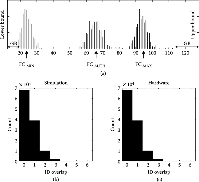
FIGURE 17.11 Hardware results. (a) Measured ID distribution with CHALLENGE of FCMIN = 25, FCMAX = 95, and FCAUTH = 65. ID overlap for different IDs: (b) Monte Carlo simulation and (c) measured results. (Rosenblatt, S. et al., Field tolerant dynamic intrinsic chip ID using 32 nm high-K/metal gate SOI embedded DRAM, IEEE J. Solid-State Circuits, 48[4], © 2013 IEEE.)
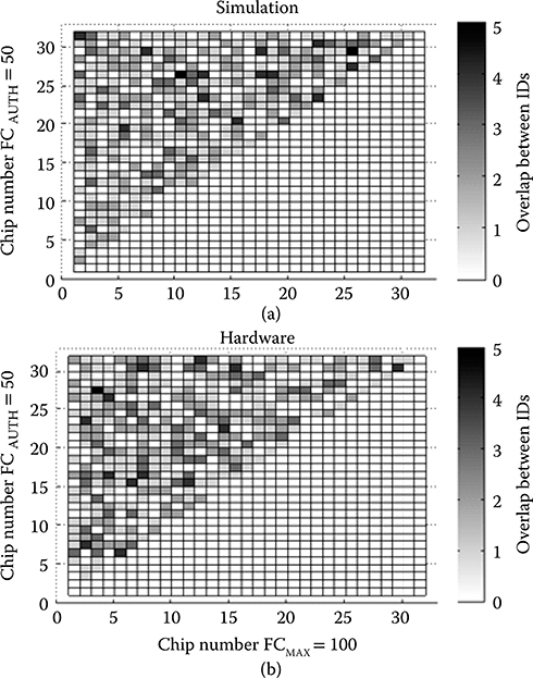
FIGURE 17.12 (a) Simulation and (b) hardware fbit overlap count by chip for FCMAX = 100 and FCAUTH = 50.
Successful recognition may be achieved even if some unstable fbits change due to variations in field test conditions and/or device shifts over the product’s lifetime, for example, NBTI [48]. As discussed in the dynamic ID approach (a), the field-tolerant approach (b) must also keep the number of retention fails, FCAUTH, less than that of a predetermined maximum value—roughly half the total array bits—to avoid false positive authentication or ID spoofing. This limit comes from the fact that a binary string with many fbits is in itself a combination of many different binary strings with fewer fbits. Therefore, there are more chances of multiple IDGEN combining to form a larger IDAUTH, or of an attacker using an IDAUTH with an arbitrarily large number of fbits for spoofing.
The field-tolerant approach requires choosing proper array and ID sizes to avoid false authentication. Although false negative authentication is the main goal of this approach, an increase in retention FC will also increase the probability of false-positive authentication, in which a chip is recognized as a different chip in the database. For randomly generated IDs, this probability is modeled by the number of expected fbits in common within any pair of IDs belonging to the set of stored IDs. Given a string representing 100 random FAIL locations in 4096 bits, the probability that another similar random string has k fails in common with the first obeys the well-known and documented hypergeometric distribution [49]. This can be interpreted as all the ways of choosing k FAIL locations in common with the original 100 while simultaneously choosing the remaining 100-k FAIL locations from the remaining 4096-100 passing locations, and it is given by:
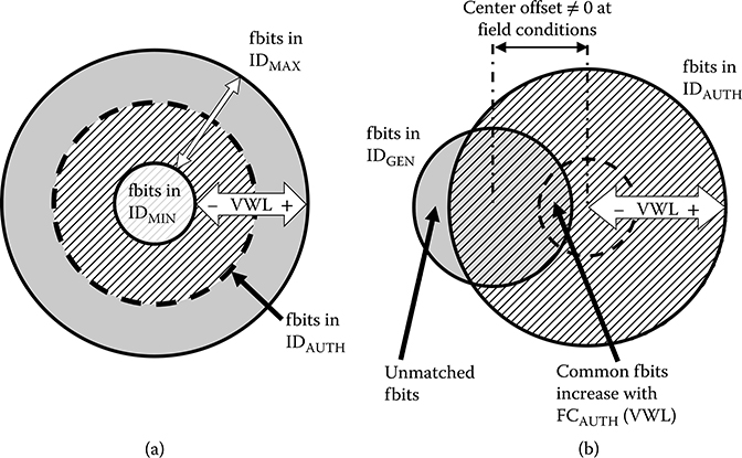
FIGURE 17.13 Concept of dynamic and field-tolerant ID approaches. Dynamic ID (a) uses IDMIN and IDMAX to improve ID security. Field-tolerant ID (b) detects common failing bits (fbits) while accepting some unmatched fbits that may be the result of a different environment in the field. (Rosenblatt, S. et al., Field tolerant dynamic intrinsic chip ID using 32 nm high-K/metal gate SOI embedded DRAM, IEEE J. Solid-State Circuits, 48[4], © 2013 IEEE.)
Using these parameters, the mean of the distribution is 2.44 common bits; therefore, most of these strings have very little ID overlap (see Table 17.3).
The calculated probability density function P(k) of 100-bit ID pairs as a function of the k overlapping fbits and array size i is shown in Figure 17.14. The function peaks near the theoretical mean of the distribution. The solid lines represent fixed 100-bit IDs, whereas the dashed lines represent the actual hardware distribution with an average over all ID sizes in a 90- to 110-bit window (accomplished by additional averaging of the function over that range). The level of accuracy in meeting the target FC is therefore expected to affect the value of the mean (peak) and the tightness of the distribution of overlapping fails (standard deviation).
Table 17.3 Probability ofd Collisions between Two IDs from Array of Sizei
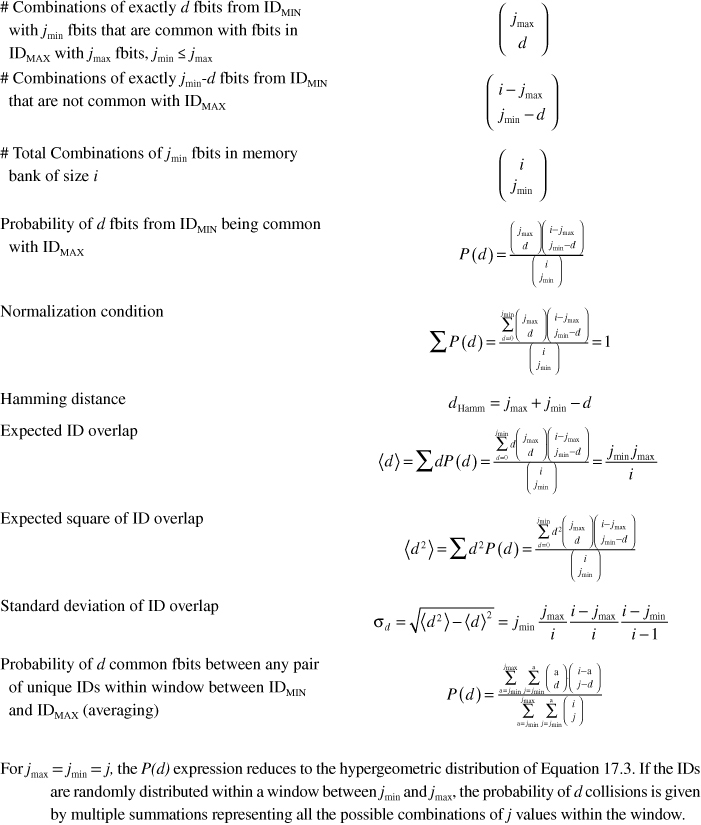
For jmax = jmin = j, the P(d) expression reduces to the hypergeometric distribution of Equation 17.3. If the IDs are randomly distributed within a window between jmin and jmax, the probability of d collisions is given by multiple summations representing all the possible combinations of j values within the window.
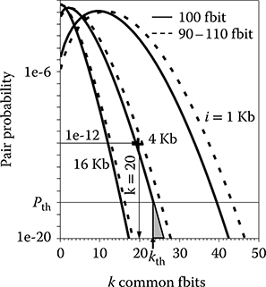
FIGURE 17.14 Calculated probability to have the corresponding ID overlap with respect to ID bit string length (i = 1 Kb, 4 Kb, and 16 Kb). (Rosenblatt, S. et al., Field tolerant dynamic intrinsic chip ID using 32 nm high-K/metal gate SOI embedded DRAM, IEEE J. Solid-State Circuits, 48[4], © 2013 IEEE.)
Statistical extrapolation can be used to establish a proper guard band of common bits kth for false positive prevention. For a set of 106 parts, the total number of pairs is on the order of 106 × 106 = 1012. Referring to the 4-Kb distribution of Figure 17.14, the odds of 1 occurrence in 1012 pairs correspond to a probability of 10−12, which in turn occurs when the number of common fbits is k = 20. By construction, the probability from the model of finding a pair within the set with more than 20 common fbits decreases exponentially. Because this model is also derived from a discrete probability curve, it is reasonable to assume that the cumulative probability above this point never adds to the probability of the point itself. To illustrate this, kth = 23 fbits in common represents a probability P(kth) = Pth that is roughly 5 orders of magnitude lower than that of 20 fbits in common. This probability also corresponds to the shaded area to the right of kth. Therefore, if no ID is ever authenticated with less than 23 fbits in common, this represents a guard band providing over 105 lower odds (Pth = 10−17) than finding 1 pair with 20 common fbits in a set of 106 parts. In other words, the final guard-banded threshold therefore satisfies unique chip IDs 99.999% (1.0–10-5) of the time for 106 parts.
To ensure 100% successful authentication, hardware analysis using voltage and temperature fluctuations must be used to take into account unstable retention fails and prevent a false negative result.
17.8 Field-Tolerant Hardware Authentication
Field-tolerant intrinsic ID generation and authentication have been demonstrated using 32 nm SOI eDRAM product IP. The 4 Kb IDGEN bit strings with target of 100 retention fails were extracted using a 4-Kb SEG from a 292-Kb array in each of 266 eDRAM chips. A nominal voltage condition of VDD = 0.9 V and 85°C was used. These IDGEN bit strings identifying each one of the 266 chips were recorded in the local database.
Field-tolerant authentication was then emulated with IDAUTH string generation for a target of 200 retention fails using the same 4-Kb SEGs. Two temperatures, 25°C and 85°C, and three voltage conditions of VDD = 0.9 V ± 10%, representative of voltage tolerance in the field, were used. The six-generated IDAUTH from each of the 266 chips were used to search the corresponding chips with previously stored IDGEN in the local database.
In searching for false positives in hardware, every IDAUTH (total 6 × 266 = 1596) was compared to the stored 266 IDGEN of a different chip as shown in Figure 17.15 for a total of approximately 420 k (= 266 × 1596) pairs. The normalized count of common fbits is overlaid with the hypergeometric model of (3) with no fitting parameters. The model assumes that the set of stored IDs have 100 random target fails (FCGEN = 100) and the set of authentication keys have 200 random target fails (FCAUTH = 200), with a +/–10% FC tolerance window for each set. The excellent agreement with the random fail model is a measure of the uniqueness and randomness of the set of IDs.
False negative authentication occurs when a previously stored chip ID cannot be recognized because of physical instability of the bit cells in the field. False negatives were characterized by comparing each IDAUTH to the stored IDGEN of the same chip. The results are summarized in Figure 17.16 for all 266 chips. No more than 10% of fbits in the authentication set fail to match the original ID. Most fbit loss occurs at 25°C, and as recorded ID size approaches authentication ID size. Tighter FC control can be used to limit this problem.
Whereas false negative characterization depends on the physical properties of the circuit and the test methodology, false positives rely on the randomness of the ID set and can be characterized with use of the model of (3). Conservatively, it is sufficient to use as few fbits as possible for recognition, as long as it ensures that all parts can be successfully authenticated without misrecognition. For 106 parts, an approach requiring that a minimum of approximately 40% of the bits from the stored IDGEN (40 fbits for 100-fail FCGEN target) are common with the authentication key IDAUTH of a different chip (200-fail FCAUTH target) guarantees authentication with at least 99.999% success rate. On the other hand, security is enhanced when a larger number of fbits is used for recognition, as it makes counterfeiting harder. Unfortunately, false negative results are made more likely by increasing the number of fbits that must be regenerated. As no more than 90% of the stored IDGEN fbits can be ensured to match the IDAUTH fbits in the simulated field authentication of Figure 17.16 while avoiding a false negative, the resulting 40%–90% window of overlapping fbits contains all the redundant authentication fbits for this hardware. A compromise between false authentication boundaries can be therefore reached with a fixed 65% fbit target to be used for field-tolerant authentication.
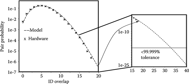
FIGURE 17.15 Probability to have the corresponding ID overlap for any of approximately 420 K pairs. A 40% overlap between a 100-fail stored ID and a 200-fail authentication key is sufficient to guarantee 99.999% ID uniqueness for 106 parts. Fail count windows of +/–10% are ensured with a +/–5 mV VWL window. (Rosenblatt, S. et al., Field tolerant dynamic intrinsic chip ID using 32 nm high-K/metal gate SOI embedded DRAM, IEEE J. Solid-State Circuits, 48[4], © 2013 IEEE.)
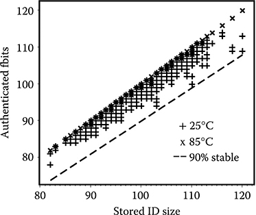
FIGURE 17.16 Measured ID overlap for each of the same 266 chips during authentication using VDD = 0.9 V and VDD = 0.9 V +/–10%, at 25°C and 85°C (total 6 conditions). The results show at least 90% of the ID string 1 bits are stable even if the test condition is changed. (Rosenblatt, S. et al., Field tolerant dynamic intrinsic chip ID using 32 nm high-K/metal gate SOI embedded DRAM, IEEE J. Solid-State Circuits, 48[4], © 2013 IEEE.)
Use of larger keys for authentication can further reduce the number of unstable fbits that are not matched by forcing those weak cells to fail eventually. As all cells will fail for sufficiently high VWL or retention time, the target value must be bounded to ensure uniqueness of the set and can be calculated using the hypergeometric model. A composite field-tolerant/dynamic key approach follows: a 200-fbit ID needs only to match roughly 65% of fbits in a 100-fbit ID, whereas having only 65% of its fbits in common with a 400-fbit maximum ID is also stored to improve security.
17.9 Security and Authentication Enhancement for Intrinsic Chip ID
The field-tolerant approach with common fbit-detection scheme enables chip authentication even if some of the bits change in a field condition. This approach, however, may turn problematic if the ID generated for authentication includes many new fails instead of reproducing most of the old ones, because that can significantly reduce the common bit ratio. Although isolated random single-bit fails are ideally suited for the field-tolerant approach, the appearance of block fails along WLs or BLs is a major source of concern and can result in false negative authentication. Some of these fail signatures, when caused by noise or soft errors, may still be recovered by test repetition. However, when these fails are caused by aging and stress, they may not be recoverable. This results in rendering the array from which the ID is collected unrecognizable.
Figure 17.17 shows the authentication and security enhancement approach. Unlike the intrinsic chip ID approach demonstrated using one 4-Kb ID per chip, an alternative approach uses multiple IDs for authentication. The approach (a) uses two IDs (ID0 and ID1), each having 4-Kb intrinsic binary strings, as a pair. The pair (with combined binary strings totaling 8 Kb) can be generated by choosing two 4-Kb SEGs from a memory array such that the two different 4-Kb intrinsic BITMAPs can be obtained. Both ID0 and ID1 are unique relative to any other IDs from different chips. The ID0 and ID1 pair is then stored in the OEM’s database. Authentication is realized by regenerating the ID0 and ID1 pair on request from the OEM. The regenerated ID0 and ID1 pair is sent to the OEM database as a response. The OEM database then checks if the IDs are the same as the respective ID0 and ID1 in the OEM database, independently. A successful authentication result is given if at least one of the IDs has a positive match. Given that odds of such block fails are very low for actual products meeting the technology reliability requirements, the odds that these failure modes may occur in several segments simultaneously are vanishingly small. This fact allows one of the IDs (i.e., ID0) to serve as a backup ID for the other (i.e., ID1), successfully authenticating the chip as long as one of the IDs remains good. This ID pair authentication approach is simple enough and extendable to authentication with multiple IDs resulting in more than one backup ID per chip. However, this increases both the overhead of ID volume and the computing power required for authentication, as the number of ID searches and comparisons increases as the number of backup IDs is increased.
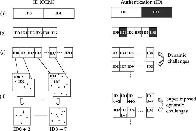
FIGURE 17.17 Security enhancement approaches using multi-IDs, micro-IDs, and bitmap superposition methods. (a) Two ID approach. Positive authentication is given if at least one of the two IDs has a positive match. (b) Micro-ID approach using six ID0-5. Positive authentication is given if at least four out of six micro-IDs (for any combination) are found in the database. (c) Dynamic chip authentication using 12 micro-IDs. Authentication is realized by providing a dynamic CHALLENGE to the chip, which identifies a selection of 8 out of 12 micro-IDs. (d) Superimposed micro-ID approach using dynamic authentication. At least two of the micro-IDs selected from a dynamic CHALLENGE are superimposed with the ID.
The micro-multiple ID approach (b) subdivides the ID into more and smaller ID segments (i.e., ID0–5). Similar to the backup approach, the OEM database stores all micro-IDs (i.e., ID0–5), each having 1-Kb binary strings. The total required ID space per chip is hence 6 Kb, which is overall smaller than that of the backup approach with two full sets of 4-Kb IDs (total 8 Kb per chip). Authentication is realized by comparing each of the 1-Kb micro-IDs with those in the OEM database. A positive authentication result is given if at least four out of six micro-IDs are found in the database. Successful authentication may happen even if two of the micro IDs do not match because of an uncoverable field failure. In addition, the ID search in the OEM database can be executed in parallel using small IDs, resulting in less computing power.
More than a backup solution, the micro-ID approach offers additional levels of security when coupled with a dynamic CHALLENGE system similar to the dynamic chip ID authentication discussed in Section 17.5. The chip is authenticated by using more than six micro-IDs (12, for example), each chip having 512b, as shown in Figure 17.17c. All 12 micro IDs (combined binary strings totaling 6 Kb) are stored in the OEM database. Authentication is realized by providing the dynamic CHALLENGE to the chip, which identifies a selection of 8 of the 512b micro-IDs. This results in approximately 20 million different 4-Kb IDs when order is taken into account, only one of which is the correct 4-Kb binary string corresponding to CHALLENGE. As the dynamic CHALLENGE changes at each authentication request, the ID used in the previous attempt is rendered invalid, consequently improving an authentication security. For example, if the CHALLENGE <1,3,4,…,0> is used in the first authentication request, a subsequent CHALLENGE <5,7,9,….3> renders the first one invalid, which prevents an attacker from attempting to spoof the ID by reusing the previous response.
The dynamic micro-ID approach can be made further secure by superimposing two or more microarray BITMAPs to create one corresponding micro-ID. For example, two of 512b BITMAPs from ID0 and ID2 are superimposed, generating a single 512b micro-ID (ID 0+2). Similarly to the micro-ID approach, a sequence of eight micro-IDs can be generated from superimposing one to at most eight of the original micro-IDs. The CHALLENGE selects the eight micro-IDs and which BITMAPs to be superimposed. The chip then sends to the OEM the string of superimposed micro-IDs as a RESPONSE, which acts as a pseudoencryption function. Simultaneously, the OEM also generates its own expected RESPONSEs from the stored micro-IDs from every chip and then compares the chip’s RESPONSE to its own ones until the chip is found in the database.
Another level of security is provided as a secret ID. Instead of targeting reliability issues, this application can be used to foil an attack by a counterfeit chip. If a fake chip tries to replicate individual micro-IDs, a suspicious OEM can choose to authenticate another micro-ID that was not disclosed during a previous authentication request. The intrinsic ID approach using memory arrays can generate a large number of micro-IDs, and is overhead-free for chip design. The micro-ID and superimposed micro-ID approaches can be combined with the backup ID approach with additional micro-IDs, and may include a field-tolerant approach to overcome some unstable fbits within the micro-ID.
17.10 Summary
In this chapter, intrinsic ID generation and authentication using a VLSI chip has been covered at length. As discussed, the approach may preferably use an intrinsic feature relating to retention fails using eDRAM. The DRAM cell allows for retention fails to be controlled by changing the subthreshold leakage. This results in generation of a skewed binary string, having more 0 bits than 1 bits, where 1 is associated with the memory array cell location causing a fail in the bitmap. The challenge of employing retention fails for the generation of intrinsic ID binary strings is how to generate a stable retention fail. This requires operating the device in the subthreshold domain, and can be realized by controlling the wordline low voltage with FC feedback during the retention test. One consequence of this FC feedback method is that the intrinsic ID can be changed dynamically as the FC target changes at each authentication request, resulting in enhanced hardware security. The discussion further includes a method to improve successful authentication rates in a field using a fuzzy match detection approach [15,16], as well as a multi-ID backup option, while further improving the dynamic micro-ID approach with superimposed BITMAPs.
Most of the ideas discussed in this chapter use intrinsic ID for chip identification to protect the product from counterfeiting. However, the applications of intrinsic ID are not limited to chip identification. As an intrinsic chip ID cannot be easily copied, one of its most technologically relevant applications is as a cryptographic key [34,35]. Unlike the intrinsic ID approach for chip identification, cryptographic keys require 100% stable and secure ID bit-string generation, which in turn requires innovations such as advanced circuit design for ID generation and authentication, while integrating the error correction code within the chip [36]. To further improve security, implementation of a reconfigurable PUF [37] that limits multiple use of the secret key may also be of special relevance. In addition to the cryptographic key challenge, a standardization of the intrinsic ID should be strongly encouraged to disseminate the use of intrinsic ID in various products. This requires the development of an intrinsic ID engine that can be embedded into any VLSI chip. This engine must take into consideration the system architecture to maximize the hardware security advantage [33]. Intrinsic ID is an emerging technology that can greatly benefit from tight interactions among technologists, circuit and system designers, and security engineers.
References
1. S. Narasimha, P. Chang, C. Ortolland, D. Fried, E. Engbrecht, K. Nummy, P. Parries et al., 22 nm High-performance SOI technology featuring dual-embedded stressors, epi-plate high-K deep-trench embedded DRAM and self-aligned via 15LM BEOL, IEEE IEDM, San Francisco, CA, 2012.
2. W. Diffie and M. Hellman, New directions in cryptography, IEEE Transactions on Information Theory, 22(6), 644–654, 1976.
3. N. Potlapally, Hardware security in practice: Challenges and opportunities, 2011 IEEE International Symposium on Hardware-Oriented Security and Trust (HOST), pp. 93–97, San Diego, CA, 2011.
4. L. Dong, K. Chen, M. Wen, Y. Zheng, Protocol Engineering Principles for Cryptographic Protocols Design, Eighth ACIS International Conference on Software Engineering, Artificial Intelligence, Networking, and Parallel/Distributed Computing (SNPD), 3: 641–646, 2007.
5. R. King. (2010, March 1). Businessweek [Online]. Available at http://www.businessweek.com/technology/special_reports/20100302ceo_guide_to_counterfeit_tech.htm.
6. R. T. Smith, J. D. Chlifala, J. F. M. Bindels, R. G. Nelson, F. H. Fischer, and T. F. Mantz, Laser programmable redundancy and yield improvement in a 64K DRAM, IEEE Journal of Solid-State Circuits, 16(5): 506–514, 1981.
7. N. Robson, J. Safran, C. Kothandaraman, A. Cestero, X. Chen, R. Rajeevakumar, A. Leslie, D. Moy, D. T. Kirihata, and S. Iyer, Electrically programmable fuse (eFUSE): From memory redundancy to autonomic chips, IEEE Custom Integrated Circuits Conference, pp. 799–804, San Jose, CA, 2007.
8. J. Safran, A. Leslie, G. Fredeman, C. Kothandaraman, A. Cestero, X. Chen, R. Rajeevakumar et al., A Compact eFUSE Programmable Array Memory for SOI CMOS, 2007 IEEE Symposium on VLSI Circuits, pp. 72–73, Kyoto, Japan, 2007.
9. G. Uhlmann, T. Aipperspach, T. Kirihata, K. Chandrasekharan, Y. Z. Li, C. Paone, B. Reed et al., A commercial field-programmable dense eFUSE array memory with 99.999% sense yield for 45 nm SOI CMOS, ISSCC Digest of Technical Papers, pp. 406–407, San Francisco, CA, 2008.
10. C. Deml, M. Jankowski, and C. Thalmaier, A 0.13 μm 2.125 MB 23.5ns Embedded flash with 2GB/s read throughput for automotive microcontrollers, ISSCC Digest of Technical Papers, pp. 478–479, San Francisco, CA, 2007.
11. H. Hidaka, Evolution of embedded flash memory technology for MCU, 2011 IEEE International Conference on IC Design & Technology (ICICDT), pp. 1–4, Kaohsiung, China, 2011.
12. R. S. Pappu. Physical one-way functions, PhD thesis, Massachusetts Institute of Technology, Cambridge, MA, 2001.
13. R. Maes, V. Rožić, I. Verbauwhede, P. Koeberl, E. van der Sluis, and V. van der Leest, Experimental evaluation of physically unclonable functions in 65 nm CMOS, Proceedings of the ESSCIRC, pp. 486–489, Bordeaux, France, 2012.
14. P. Simons, E. van der Sluis, and V. van der Leest, Buskeeper PUFs, a promising alternative to D Flip-Flop PUFs, 2012 IEEE International Symposium on Hardware-Oriented Security and Trust (HOST), pp. 7–12, San Francisco, CA, 2012.
15. G.-J. Schrijen and V. van der Leest, Comparative analysis of SRAM memories used as PUF primitives, Design, Automation & Test in Europe Conference & Exhibition (DATE), pp. 1319–1324, Dresden, Germany, 2012.
16. G. Selimis, M. Konijnenburg, M. Ashouei, J. Huisken, H. de Groot, V. van der Leest, G.-J. Schrijen, M. van Hulst, and P. Tuyls, Evaluation of 90 nm 6T-SRAM as physical unclonable function for secure key generation in wireless sensor nodes, 2011 IEEE International Symposium on Circuits and Systems (ISCAS), pp. 567–570, Rio de Janeiro, Brazil, 2011.
17. Y. Su, J. Holleman, and B. Otis, A 1.6pJ/bit 96% stable chip-ID generating circuit using process variations, ISSCC Digest of Technical Papers, pp. 406–611, San Francisco, CA, 2007.
18. D. Holcomb, W. P. Burleson, and K. Fu, Power-up SRAM state as an identifying fingerprint and source of true random numbers, IEEE Transactions on Computers, 58(9): pp. 1198–1210, 2009.
19. M. Cortez, A. Dargar, S. Hamdioui, and G.-J. Schrijen, Modeling SRAM start-up behavior for physical unclonable functions, 2012 IEEE International Symposium on Defect and Fault Tolerance in VLSI and Nanotechnology Systems (DFT), pp. 1–6, Austin, TX, 2012.
20. H. Handschuh, Hardware-anchored security based on SRAM PUFs, Part 1, IEEE Security & Privacy, 10(3): 80–83, 2012.
21. H. Handschuh, Hardware-anchored security based on SRAM PUFs, Part 2, IEEE Security & Privacy, 10(4): 80–81, 2012.
22. S. Chellappa, A. Dey, and L. T. Clark, Improved circuits for microchip identification using SRAM mismatch, IEEE Custom Integrated Circuits Conference, pp. 1–4, San Jose, CA, 2011.
23. H. Fujiwara, M. Yabuuchi, H. Nakano, H. Kawai, K. Nii, and K. Arimoto, A chip-ID generating circuit for dependable LSI using random address errors on embedded SRAM and on-chip memory BIST, Symposium On VLSI Circuits, pp. 76–77, Honolulu, HI, 2011.
24. C. Costea, F. Bernard, V. Fischer, and R. Fouquet, Analysis and enhancement of ring oscillators based physical unclonable functions in FPGAs, 2010 International Conference on Reconfigurable Computing and FPGAs, pp. 262–267, Quintana Roo, 2010.
25. G. E. Suh and S. Devadas, Physical unclonable functions for device authentication and secret key generation, 44th ACM/IEEE Design Automation Conference (DAC’07), pp. 9–14, San Diego, CA, 2007.
26. D. Lim, J. W. Lee, B. Gassend, G. E. Suh, M. van Dijk, and S. Devadas, Extracting secret keys from integrated circuits, IEEE Transactions on Very Large Scale Integration (VLSI) Systems, 13(10): 1200–1205, 2005.
27. K. Lofstrom, W. R. Daasch, and D. Taylor, IC identification circuit using device mismatch, ISSCC Digest Technical Papers, pp. 372–373, San Francisco, CA, 2000
28. N. Liu, S. Hanson, D. Sylvester, and D. Blaauw, OxID: On-chip one-time random ID generation using oxide breakdown, 2010 IEEE Symposium on VLSI Circuits (VLSIC), pp. 231–232, Honolulu, HI, 2010.
29. J. Ju, J. Plusquellic, R. Chakraborty, and R. Rad, Bit string analysis of physical unclonable functions based on resistance variations in metals and transistors, 2012 IEEE International Symposium on Hardware-Oriented Security and Trust (HOST), pp. 13–20, San Francisco, CA, 2012.
30. M. Yu, R. Sowell, A. Singh, D. M’Raihi, and S. Devadas, Performance metrics and empirical results of a PUF cryptographic key generation ASIC, IEEE Symposium on Hardware-Oriented Security and Trust (HOST), pp. 108–115, San Francisco, CA, 2012.
31. D. Fainstein, S. Rosenblatt, A. Cestero, J. Safran, N. Robson, T. Kirihata, and S. S. Iyer Dynamic intrinsic chip ID using 32 nm high-K/metal gate SOI embedded DRAM, IEEE Symposium on VLSI Circuits, pp. 146–147, Honolulu, HI, 2012.
32. S. Rosenblatt, D. Fainstein, A. Cestero, J. Safran, N. Robson, T. Kirihata, and S. S. Iyer, Field tolerant dynamic intrinsic chip ID using 32 nm high-K/metal gate SOI embedded DRAM, IEEE Journal of Solid-State Circuits, 48(4): 940–947, 2013.
33. S. Rosenblatt, D. Fainstein, A. Cestero, N. Robson, T. Kirihata and S. S. Iyer, A self-authenticating chip architecture using an intrinsic fingerprint of embedded DRAM, IEEE Journal of Solid-State Circuits, 48(11): 2934–2943, 2013.
34. V. van der Leest, B. Preneel, E. van der Sluis, Soft decision error correction for compact memory-based PUFs using a single enrollment, Cryptographic Hardware and Embedded Systems (CHES), Lecture Notes in Computer Science 7428: 268–282, 2012.
35. V. van der Leest, E. van der Sluis, G.-J. Schrijen, P. Tuyls, and H. Handschuh, Efficient implementation of true random number generator based on SRAM PUFs, Cryptography and Security: From Theory to Applications, Lecture Notes in Computer Science, 6805: 300–318, 2012.
36. Z. Paral and S. Devadas, Reliable PUF value generation by pattern matching, USA Patent US 2012/0183135 A, 2012.
37. S. Katzenbeisser, Ü. Koçabas, V. van der Leest, A.-R. Sadeghi, G.-J. Schrijen, H. Schröder, C. Wachsmann, Recyclable PUFs: Logically reconfigurable PUFs, Cryptographic Hardware and Embedded Systems (CHES) 2011, Lecture Notes in Computer Science, 6917: 374–389, 2011.
38. T. Kirihata, High-performance embedded dynamic random access memory in nano-scale technologies, In CMOS Processors and Memories, edited by K. Iniewski, pp. 295–336, Springer: Dordrecht, Heidelberg, London, New York, ISBN 978-90-481-9215-1, 2010.
39. D. Wendel, R. Kalla, J. Warnock, R. Cargnoni, S. G. Chu, J. G. Clabes, D. Dreps et al., POWER7™, a highly parallel, scalable multi-core high end server processor, IEEE Journal of Solid-State Circuits, 46(1): 145–161, 2011.
40. S. Rusu, S. Tam, H. Muljono, J. Stinson, D. Ayers, J. Chang, R. Barada, M. Ratta, S. Kottapalli, and S. Vora, A 45 nm 8-core enterprise XEONR processor, IEEE Journal of Solid-State Circuits, 45(1): 7–14, 2010.
41. J. Barth, D. Plass, E. Nelson, C. Hwang, G. Fredeman, M. Sperling, A. Mathews et al., A 45 nm SOI embedded DRAM macros for POWER7TM processor 32 MByte on-chip L3 cache, IEEE Journal of Solid-State Circuits, 46(1): 64–75, 2011.
42. M. Takeuchi, K. Inoue, M. Sakao, T. Sakoh, T. Kitamura, S. Arai, T. Iizuka et al., A 0.15 μm logic based embedded DRAM technology featuring 0.425 μm2 stacked cell using MIM (metal–insulator–metal) capacitor, Symposium on VLSI Technology, Digest Technical Papers, Kyoto, Japan, pp. 29–30, 2001.
43. G. Bronner, H. Aochi, M. Gall, J. Gambino, S. Gernhardt, E. Hammerl, H. Ho et al., A fully planarized 0.25 μm CMOS technology for 256Mb DRAM and beyond, Symposium on VLSI Technology, Digest Technical Papers, Kyoto, Japan, pp. 15–16, 1995.
44. J. B. Kuang, A. Mathews, J. Barth, F. Gebara, T. Nguyen, J. Schaub, K. Nowka et al., An on-chip dual supply charge pump system for 45 nm eDRAM, ESSCIRC 2008, pp. 66–69, Edinburgh, United Kingdom, 2008.
45. J. Golz, J. Safran, H. Bishan, D. Leu, Y. Ming, T. Weaver, A. Vehabovic et al., 3D stackable 32 nm high-K/metal gate SOI embedded DRAM prototype, IEEE Symposium on VLSI Circuits, pp. 228–229, Honolulu, HI, 2011.
46. J. Warnock, Y. H. Chan, H. Harrer, D. Rude, R. Puri, S. Carey, G. Salem et al., 5.5 GHz System z microprocessor and multichip module, IEEE International Solid-State Circuits Conference (ISSCC), pp. 46–47, San Francisco, CA, 2013.
47. A. AI-Rawi, A. Lansari, and F. Bouslama, A new non-recursive algorithm for binary search tree traversal, Proceedings of the 2003 10th IEEE International Conference on Electronics, Circuits and Systems (ICECS), 2: 770–773, 2003
48. T. Yamamoto, K. Uwasawa, and T. Mogami, Bias temperature instability in scaled p+ polysilicon gate p-MOSFETs, IEEE Transactions on Electron Devices, 46(5): 921–926, 1999.
49. W. Feller, The hypergeometric series, In An Introduction to Probability Theory and Its Applications, 3rd Ed., Vol. 1, pp. 41–45. New York: Wiley, 1968.