
16 Very-Large-Scale Integration Implementations of Cryptographic Algorithms
Tony Thomas
Contents
16.2 VLSI Implementations of Cryptographic Primitives
16.3 VLSI Implementation of RC4 Stream Cipher
16.3.1 RC4 Stream Cipher Algorithm
16.4 VLSI Implementation of Data Encryption Standard Block Cipher
16.4.1 Data Encryption Standard Block Cipher Algorithm
16.4.2 Triple Data Encryption Standard Implementation
16.5 VLSI Implementation of Advanced Encryption Standard Block Cipher
16.5.1 Advanced Encryption Standard Algorithm
16.5.2 Advanced Encryption Standard Implementation
16.6 VLSI in RSA Asymmetric-Key Cryptosystem
16.6.1 RSA Encryption and Decryption Algorithms
16.7 VLSI Implementation of Elliptic Curve Cryptosystem
16.7.1 Elliptic Curve Cryptography
16.7.2 Elliptic Curve Cryptosystem Implementation
16.1 Introduction
Today secure storage and transfer of information as well as communication over Internet and mobile networks has become very critical. Cryptographic algorithms have been developed to provide various security services such as confidentiality, user authentication, data origin authentication, data integrity, nonrepudiation, privacy, and so on. Cryptographic algorithms are divided into two categories: symmetric-key or secret-key algorithms and asymmetric-key or public-key algorithms. Symmetric-key cryptography refers to cryptographic mechanisms in which both the sender and receiver share the same key or keys that are related in an easily computable way. In asymmetric-key cryptography, two different but mathematically related keys (not in an easily computable way) called public and private keys are used. A public-key cryptosystem is constructed in such a way that calculation of the private key is computationally infeasible from the public key.
The rapid growth of portable electronic devices with limited power and area, such as mobile phones and smart cards, has opened up the necessity to carry out the very-large-scale integration (VLSI) hardware implementations of cryptographic algorithms on low-power and compact circuits. Unlike the usual computer and network security systems that impose less stringent limitations on the area and power consumption, portable devices impose more restrictions on area and power and less on throughput. This difference in requirements necessitates a different approach in the design and implementation of the cryptographic algorithms for these devices. Thus, to be fast and feasibly practical as well as to satisfy conflicting requirements of power, area, and throughput in the security applications, cryptographic algorithms have to be implemented in hardware. Dedicated hardware devices can run encryption routines concurrently with other applications in the host computer. As hardware solutions are tamper proof, hardware implementations of cryptographic algorithms ensure confidentiality, integrity, and authentication of cryptographic keys. This makes the cryptographic keys to be safely stored inside the hardware. On the other hand, software implementations of cryptographic algorithms are prone to manipulations and a dedicated attacker may be able to reverse engineer the cryptographic keys. However, hardware is more expensive than software and memory is a constraint in hardware designs. Hence, the algorithms must be specially tailored for hardware implementations. The cryptographic algorithms should be made compact, scalable, and modular to reduce the overall cost of the hardware required.
Because, present-day multipurpose smart cards are used for a wide range of applications, they must support both symmetric-key and asymmetric-key cryptographic algorithms. Symmetric-key algorithms with high throughput are suitable for data communication, whereas asymmetric-key algorithms with lower throughput are suitable for key exchange and authentication protocols. Among various cryptographic algorithms, approved standards such as RC4, Data Encryption Standard (DES), Triple Data Encryption Standard (3DES), Advanced Encryption Standard (AES), RSA, Elliptic curve cryptosystem (ECC), SHA-3, and so on are used for these applications. RC4, for encryption of stream of data, DES/3DES, for past compatibility, and AES, for high security and throughput, are the major symmetric-key algorithms used. ECC, for high encryption efficiency, is the best candidate for asymmetric-key encryption, and SHA-3 is used in integrity applications.
This chapter focusses on the VLSI implementations of various cryptographic algorithms. The rest of this chapter is organized as follows. In Section 16.2, we introduce various cryptographic primitives and discuss the importance of VLSI implementation of such primitives. In Sections 16.3 through 16.5, we discuss the VLSI implementations of symmetric-key ciphers RC4, DES, and AES, respectively. In Sections 16.6 and 16.7, we discuss the VLSI implementations of asymmetric-key ciphers RSA and elliptic curve system. In Section 16.8, we discuss the VLSI implementations of SHA-3 hash function. Finally, the chapter concludes with Section 16.9.
16.2 VLSI Implementations of Cryptographic Primitives
In this section, we focus on the VLSI implementations of the cryptographic primitives such as stream ciphers, block cipher, asymmetric-key encryption algorithms, and hash functions.
A stream cipher is a symmetric key encryption algorithm where plaintext digits are combined with a pseudorandom keystream generated by the stream cipher. In a stream cipher, each plaintext bit or byte or block of any size is encrypted one at a time with the corresponding bit or byte or block of the keystream, to give the corresponding bit or byte or block of the ciphertext stream. Usually, the message stream is combined with the keystream with a bitwise exclusive-or (XOR) operation. The pseudorandom keystream is typically generated serially from a random seed value that serves as the key of the stream cipher. Many stream cipher algorithms are designed by combining the outputs of several independent Linear Feedback Shift Registers (LFSRs) using a nonlinear Boolean function. The VLSI area used in implementing such stream cipher systems has two components: the area used to implement the LFSRs and the area used to implement the Boolean function. The area required to implement the LFSRs is proportional to the product of the length of the LFSR and the number of inputs to the LFSR, whereas the area required to implement the Boolean function grows exponentially with the number of inputs. Thus, implementing the Boolean function is a main hurdle in this case.
Block ciphers operate on large blocks of data such as 128 bits with a fixed, unvarying transformation. A block cipher is a function that maps an n-bit plaintext blocks to an n-bit ciphertext block, where n is called the block length. The function is parameterized by a key K. The encryption operation involves several rounds of primitive operations such as substitution, permutations, key mixing, shifting, swapping, look-up table (LUT) reading, and so on. The decryption operation involves reversing the previously mentioned operations. The encryption and decryption algorithms use the same key. The fundamental difference between a block cipher and stream cipher is that in a block cipher, the same key is used for encrypting each block of data, whereas in a stream cipher, no key is repeated and thus different keys are used for encrypting different blocks of data. Five modes of operation are used for the block ciphers for encrypting data that is longer than a block length. Among these, three of the modes, namely Cipher Block Chaining mode (CBC), Cipher Feedback mode, and Output Feedback mode (OFB), are feedback modes, whereas the remaining two, namely Electronics Code Book mode (ECB) and Counter mode (CTR), are non-feedback modes. In the feedback modes, encryption of each block of data starts only after the completion of encryption of the previous block of data. As a result, in feedback modes all the blocks must be encrypted sequentially. On the other hand, in the non-feedback modes each block of data can encrypted independently with each other. So, in non-feedback mode, many blocks of data can be encrypted in parallel. FPGA devices are highly promising for implementing block ciphers. The fine granularity of FPGAs matches well with the operations such as permutations, substitutions, LUT reading, and the Boolean functions used by these algorithms. Furthermore, FPGA can efficiently exploit the inherent parallelism of the block cipher algorithms.
Asymmetric encryption or public-key encryption refers to a cryptographic algorithm that requires two separate keys, one of which is kept as secret and the other is made public. Although different, these two key pairs are mathematically linked. The public key is used to encrypt plaintext to the ciphertext, whereas the private key is used to decrypt ciphertext back to the plaintext. The term asymmetric refers to the use of different keys to perform these opposite functions in contrast with the conventional symmetric cryptography that relies on the same key to perform both the operations. Asymmetric-key cryptographic algorithms are based on hard mathematical problems that currently admit no efficient solutions. Examples of such problems are integer factorization problem [1], discrete logarithm problem [1,2], shortest lattice vector problem [1], conjugacy problem [3,4], and so on. The security of asymmetric key cryptography lies in the fact that it is computationally infeasible for a properly generated private key to be determined from its corresponding public key. Thus the public key can be published without compromising the security, whereas the private key must be kept secret and should not be revealed to anyone not authorized to read the messages. Asymmetric key algorithms, unlike the symmetric key algorithms, do not require a secure initial exchange of the secret key between the sender and the receiver. The main limitation of asymmetric-key algorithms is in their complexity. Asymmetric key algorithms are much more complex and slower than the symmetric key algorithms. It is widely believed that the complexity of most of the public-key algorithms make them unsuitable for resource-constrained applications. International Standard Organization has set the limit of the maximum chip area on a smart card to 25 mm. Considering the nonvolatile and volatile memories, CPU, and other peripheral circuits required on the chip, it is desirable to fit the security component in the smallest area possible.
A cryptographic hash function maps data of arbitrary length to data of a fixed length. The output values of a hash function are called hash values or hash codes or checksums or simply hashes. Hash functions are used to protect the integrity of messages using symmetric-key-based message authentication code, asymmetric-key-based digital signature, making commitments, time stamping, key updating, protecting password files, intrusion detection, and so on. Thus, besides high security, a hash function should be suitable for implementations on a wide range of applications. The hardware efficiency of a hash function will be crucial to determine its future, because hardware resources are often limited, whereas on high-end computers, it does not matter much in general. In fact, even the slowest hash function has an acceptable performance on a PC.
16.3 VLSI Implementation of RC4 Stream Cipher
RC4 is a stream cipher designed by Ron Rivest in 1987 for RSA Security. It is a variable key-size stream cipher with byte-oriented operations. The algorithm is based on the use of a random permutation where eight to sixteen machine operations are required per output byte. RC4 is used for encryption in the wired equivalent privacy protocol (part of the IEEE 802.11b wireless LAN security standard).
16.3.1 RC4 Stream Cipher Algorithm
The RC4 algorithm is a remarkably simple cipher. A variable-length key K of size 1–256 bytes (8–2048 bits) is used to initialize a 256-byte state vector S = (S[0], S1, …, S[255]). At all times, S contains a permutation of all the 8-bit numbers from 0 through 255. For encryption and decryption, a byte is selected from S in a systematic fashion. The entries in S are then once again permuted.
Initially the entries in S are set equal to the values from 0 through 255 in the ascending order, that is, S = (0, 1, …, 255). A temporary vector, T, is also created. If the length of the key K is 256 bytes, then K is copied to T. Otherwise, for a key of length keylen bytes, K is copied to the first keylen elements of T and then K is repeated as many times as necessary to fill out T.
T is then used to produce the initial permutation of S. This involves starting with S[0] and going through to S[255], and, for each S[i], swapping S[i] with another byte S[j] in S where j is computed (j is initialized 0) as j ← (j + S[i] + T[i]) mod 256.
After the initialization of vector S, the key K is no longer used. Stream generation involves starting with S[0] and going through to S[255], and, for each S[i], swapping S[i] with another byte in S according to the following scheme dictated by the current configuration of S. First i and j are initialized to 0.
i = (i + 1) mod 256
j = (j + S[i]) mod 256
Swap (S[i], S[j])
t = (S[i] + S[j]) mod 256
k = S[t]
The stream output is k, which is the key. After S[255] is reached, the process continues, starting over again at S[0]. Encryption is performed by XORing the stream output with the next byte of the plaintext. Decryption is carried out by XORing the same stream output with the next byte of the ciphertext. The stream generation by the RC4 cipher is illustrated in Figure 16.1.
16.3.2 RC4 Implementation
In Kitsos et al. [5], a hardware implementation of the RC4 stream cipher is presented. The implementation is parameterized to support variable key lengths (key length could be 8 up to 128 bits). This implementation requires three clock cycles per byte generation in the key setup phase, and three clock cycles per byte generation in the encryption phase. The total number of operations required is 768 + 3n clock cycles, where n is the number of bytes of the plaintext/ciphertext.
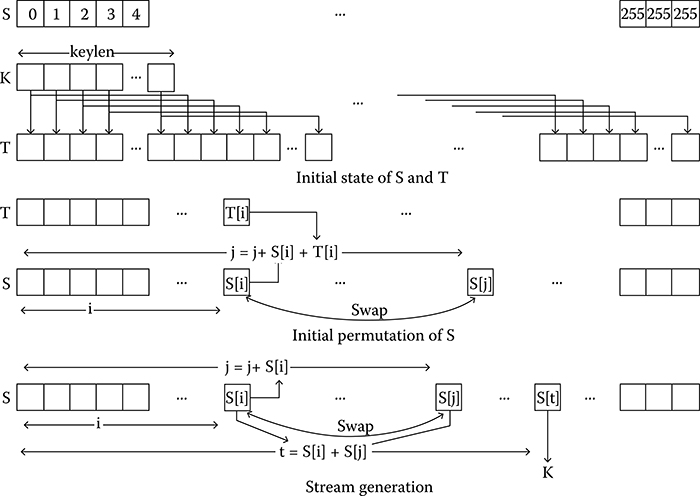
FIGURE 16.1 Stream generation by RC4 cipher.
The proposed architecture in Kitsos et al. [5] consists of a control and a storage unit. The storage unit is responsible for the key setup and generation of the key-stream. There are two 256-byte arrays, S-box and K-box. The S-box is filled with the state array and the K-box consists of the key, repeating as necessary, to fill the array. The storage unit contains memory elements for the S-box and the K-box, along with 8-bit registers, adders, and one multiplexer.
The S-box RAM consists of three 256 bytes RAM blocks with same signals of clock and reset. Each RAM block has four inputs and one output. The two inputs are the read and write signals whereas the other two are the address and the data signals. When a reset signal occurs, the blocks are initialized linearly; when the write signal occurs, new data are stored in the address position; and when the read signal occurs, the data in the address position are available on the output of the block.
At the first clock cycle, the value of the counter i is used as address in the first RAM block. The value of the register S[i] is used for the computation of the new value of j. Two adders are used for the computation of the new value of j. The input to the adders is the values of T[i] and S[i]. At the second clock cycle, the new value j is used as the address for the second RAM block. The value stored in this address is temporarily stored in the S[j] register. At the third cycle, the contents of the S[i] register and S[j] register are written in the registers at the j-th and i-th address locations, respectively.
The operations in the key setup phase are as follows. First, the value of i is used as address in the first RAM block. Then the new value of j is computed. At the second step, the new value of j is used as address of the second RAM block and the value of S[j] is stored in the j-th register. Then the values of S[i] and S[j] are added and the result of the addition is stored in the S[t] register. At the third step, the contents of the S[i] register and S[j] register are swapped and the value of the t-th register S[t] is used as address for the third RAM block. The value of S[t] is produced in the third step and this value of S[t] becomes the stream-generated key byte.
The encryption (decryption) is achieved by the bitwise XORing of the keystream with the plaintext (ciphertext). The operation of the storage unit is synchronized by a control unit and the control unit is responsible for the generation of the clock and control signals.
16.4 VLSI Implementation of Data Encryption Standard Block Cipher
The DES was published by the National Bureau of Standards in 1977 and reaffirmed in its final form by the Federal Information Processing Standards Publication (FIPS) in 1994 [6]. DES is a block cipher with Feistel networks, which operates on data blocks of 64-bit with a key of 56 (64 with 8 parity bits) bits length. DES is a 16-round cipher. Each round is identical with different round keys.
Triple DES is built on 3 DES block cipher to support a higher security level. It operates on the Encryption–Decryption–Encryption (EDE) mode, which uses sequentially a DES encryption, then a DES decryption, and finally a DES encryption, with the support of two or three different keys.
Triple DES has been used in various cryptographic applications and wireless protocol security layers. The 3DES algorithm in the EDE scheme uses both the encryption and the decryption operations. DES encryption and decryption algorithms are identical. The only difference is that the subkeys in the 16 rounds of a DES decryption have to be generated and used in the reverse order compared to the DES in the encryption mode. To produce the subkeys in reverse order, they have to be cyclically shifted right, as opposed to left for encryption.
16.4.1 Data Encryption Standard Block Cipher Algorithm
The DES algorithm in brief is as follows. Get a 64-bit block of data. Sixteen different round keys K[1], …, K[16] are first generated from the DES key K. An initial permutation is performed on the data block. The block is then divided into two halves. The first 32 bits are called the left half L[0], and the last 32 bits are called the right half R[0]. Sixteen subkeys are then applied to the data block in 16 successive rounds. Start with i = 1. The 32-bit R[i − 1] is expanded into 48 bits according to a bit-selection function E (.). E (R[i − 1]) is XORed with K[i]. E (R[i − 1]) ⊕ K[i] is then broken into eight 6-bit blocks and fed into eight S-boxes (substitution boxes). Each S-box has a 4-bit long output. Outputs from all the eight S-boxes concatenated and the bits in the resulting 32 bit string is permuted. The resulting string is XORed with L[i − 1] to get R[i − 1]. R[i − 1] is assigned as the new L[i]. The operation in the i-th round is illustrated in Figure 16.2. This process is repeated for the 16 rounds. After the 16th round, the left and right halves are swapped. Then inverse of the initial permutation is then performed on the result of left-right swap. The ciphertext is the output of the inverse permutation operation. To decrypt, use the same process, but just use the keys K[i] in the reverse order.
16.4.2 Triple Data Encryption Standard Implementation
Each DES begins with initial permutation IP and ends with the inverse of the initial permutation. These two permutations are inverse operations. When three DES are concatenated, the initial permutation of the previous DES follows the inverse initial permutation of the current DES and they cancel out. Hence, only the first IP and the last inverse IP need to be performed. As a result, the initial permutations of the second and third DES, and the final permutations of the first and the second DES, are not required to be included in the VLSI architecture. For all the following implementations of 3DES, the S-BOXes have been integrated by LUTs as well as by read-only memory (ROM) blocks.
We now describe a 48-stage VLSI architecture proposed in Kitsos et al. [7]. This architecture has the ability to process 48 independent data blocks. The subkeys for the 48 rounds are generated by three key scheduler units corresponding to the three DES components. Each key generator for a DES round produces 16 round keys. The 64-bit input key is initially permuted, and is then passed through a hardwired shifter and is finally passed through a second round permutation for each subkey. A memory of 3 × 64 bits is placed at the input to the key scheduling circuit. In this memory, the three 64 bits keys corresponding to the three DES rounds are stored to input the appropriate key in the appropriate time. On the first clock cycle, the first key is applied on the key scheduler and the DES runs in the encryption mode. On the 17th clock cycle the second key is supplied on the key scheduler and the DES runs in the decryption mode. Finally, on the 33rd cycle the third key is supplied and the DES runs in the encryption mode.
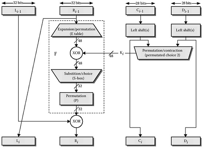
FIGURE 16.2 One round of Data Encryption Standard algorithm.
A second architecture proposed by Kitsos et al. [7] consists of 1 DES with 16 pipeline registers between the rounds. A multiplexer is used to determine between the new data and the output of the DES from the previous stage. This architecture can process 16 independent data blocks at a time. The generation of subkeys comprises 16 rounds. This architecture is suitable for high-speed applications that support ECB or automated teller machine (ATM) counter modes of operation of the block cipher where same message blocks encrypt to same ciphertext blocks.
A third architecture proposed by Kitsos et al. [7] uses consecutive iterations. Only one basic round each is implemented for the 3DES algorithm and the key scheduler to minimize the resources allocated for the 3DES. In this case, the required hardware resources are reduced by a factor of 40, 80, and 16, respectively, compared to the previous ones.
The output of the basic round is loaded to a register and another register is used for the input plaintext. The plaintext is loaded during the initialization step into the multiplexer. Feedback is used for loading new data blocks through the multiplexer for transforming the data during the 48 rounds of the 3DES. The key scheduler has one basic round and successive round subkeys are computed by simple rotations and permutations. The key scheduler provides one subkey at every clock cycle where 48 clock cycles are needed for the execution of the whole 3DES block cipher.
Because this architecture uses the minimum hardware with feedback mode, it is suitable for area-restricted devices and for the CBC or OFB modes of the block cipher operations.
16.5 VLSI Implementation of Advanced Encryption Standard Block Cipher
In January 1997, to replace the aging DES, the National Institute of Standards and Technology (NIST) invited proposals for new algorithms for the AES [8]. After two rounds of evaluation on the 15-candidate algorithms, NIST selected the Rijndael as the AES in October 2000. The AES block cipher has broad applications, in various domains such as smart cards, cellular phones, ATMs, disk security, and digital video recorders. Hardware implementations of the AES block cipher can provide better physical security as well as higher speed compared to the software implementations.
16.5.1 Advanced Encryption Standard Algorithm
AES, like DES, is an iterative algorithm. Each iteration is called a round. AES block cipher algorithm deals with data blocks of 128 bits using keys with three standard lengths of 128, 192, and 256 bits. The 128-bit data block is divided into 16 bytes. These bytes are mapped to a 4 × 4 array called the state, and all the internal operations of the AES algorithm are performed on the state matrix. The internal operations consist of mainly four primitive transformations: Sub-Bytes, ShiftRows, MixColumns, and AddRoundKey. AES encryption/decryption process involves these four primitive transformations executed iteratively in several rounds. The number of rounds is 10, 12, or 14, corresponding to the key sizes 128, 192, and 256, respectively.
In the encryption procedure, the input data is bitwise XORed with an initial key, and then four transformations are executed in the following order: Sub-Bytes, ShiftRows, MixColumns, and AddRoundKey for all rounds except the last one. All four transformations except the MixColumns transformation are performed in the last round (in the same order). The execution sequence is reversed in the decryption process, with the inverses of transformations such as InvSubBytes, InvShiftRows, InvMixColumns, respectively as well as the AddRoundKey operation. Because each round needs a round key, an initial key is used to generate all the round keys before the encryption/decryption operation. The block diagram of the AES encryption and the decryption algorithms is given in Figure 16.3.
16.5.2 Advanced Encryption Standard Implementation
Three architectural optimization approaches are usually employed to speed up the hardware implementations of AES. They are pipelining, subpipelining, and loop-unrolling. Among these three approaches, the subpipelined architecture can achieve maximum speedup and optimum speed–area ratio in non-feedback modes of the block cipher. The advantage of subpipelining can be enhanced further by dividing each round unit into more substages with equal delay. However, the SubBytes and the InvSubBytes operations in the AES algorithm are traditionally implemented by LUTs.
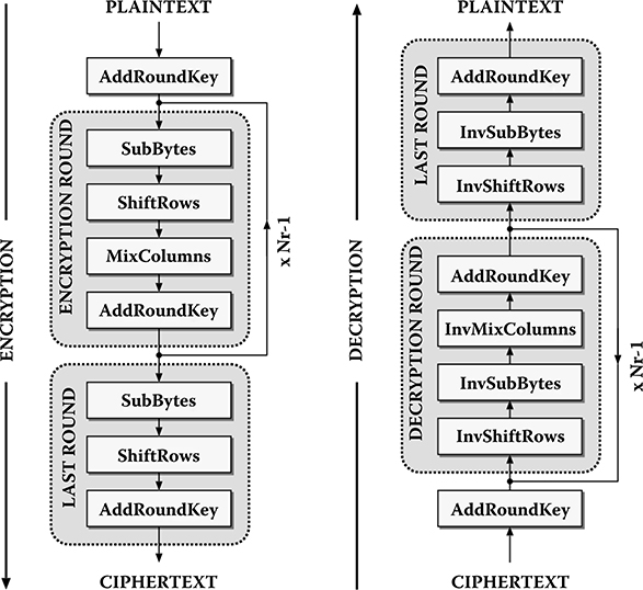
FIGURE 16.3 Advanced Encryption Standard encryption and decryption algorithms.
In Zhang et al. [9], the authors avoid the use of LUTs and propose the use of composite field data paths for the SubBytes and InvSubBytes transformations. They achieved high-speed subpipelined AES architectures through such data paths. Composite field arithmetic has been employed by Satoh et al. [10] to design efficient data paths. In the architecture proposed in Zhang et al. [9], the inversion in GF (24) is implemented by a novel approach, which leads to a more efficient architecture with shorter critical path and smaller area. The composite field arithmetic used in Rudra et al. [11] is not efficient in all the transformations used in the AES algorithm. In Zhang et al. [9], a key expansion architecture is presented, which is well suited for subpipelined designs. Further, this architecture can operate in an on-the-fly manner.
16.6 VLSI in RSA Asymmetric-Key Cryptosystem
RSA, which is also a standard and widely used asymmetric-key algorithm, is not considered in many hardware designs for the following three reasons [12]:
ECC with a key size of 160 bits provides the same level of security as RSA with a key size of 1024 bits. Thus, ECC will be a better choice when implementation area is a critical factor in the design.
RSA uses binary addition of large numbers and needs binary adders that are either slow for carry propagation or large for look-ahead carry generation.
A larger number of bits in RSA require wider buses, which adds to the area and power consumption of the design.
However, we will quickly review a VLSI implementation of RSA algorithm.
16.6.1 RSA Encryption and Decryption Algorithms
RSA is a public-key cryptographic algorithm. It uses two keys: a public key and a private key. The public key is known to everyone and is used for encrypting messages. Messages encrypted with the public key can be decrypted only using the private key. The keys for the RSA algorithm are generated in the following way:
Choose randomly two distinct prime numbers p and q of approximately equal bit length.
Compute n = pq.
Compute φ(n) = (p − 1)(q − 1), where φ is the Euler’s totient function.
Choose an integer e having a short bit length and small Hamming weight such that 1 < e < φ (n) and the greatest common divisor (e,φ(n)) = 1; that is, e and φ(n) are relatively prime. e is published as the public key exponent.
Determine d as ed ≡ 1(mod φ(n)). d is securely kept as the private key exponent.
The encryption is performed as follows. Alice sends her public key (n,e) to Bob and keeps the private key d secret. To send a message M to Alice, Bob firsts converts M into an integer m, such that 0 ≤ m < n. He then computes the ciphertext c corresponding to m as
This can be done quickly using the method of exponentiation by repeated squaring. Bob then transmits c to Alice.
On receiving the ciphertext c, Alice can recover m from c by using her private key exponent d by performing the decryption operation as
After getting m, Alice can recover the original message M by reversing the conversion operation.
16.6.2 RSA Implementation
LFSR can be used to generate random numbers p and q. Simultaneously, each number will be checked to see whether it is a prime number or not. The modular multiplication can be implemented using shift-add multiplication algorithm. The modular exponentiation can be implemented using a 16-bit modular exponentiation using LR binary method, where LR stands for the left-to-right scanning direction of the exponent.
Modular multiplication is a slightly complicated arithmetic operation because of the inherent multiplication and division operations. Modular multiplication can be carried out by performing the modulo operation after multiplication or during the multiplication. The modulo operation is accomplished by integer division, in which only the remainder after division is taken for further computation. The first approach requires an n × n bit multiplier with a 2n-bit register followed by a 2n × n bit divider. In the second approach, the modulo operation occurs in each step of integer multiplication. Therefore the first approach requires more hardware while the second requires more addition/subtraction computations. Different number representations such as redundant number systems and higher radix carry-save form have been used for this purpose. A carry prediction mechanism has also been used for fast calculation of modular multiplication.
Various authors [13,14,15,16] have proposed different array structures suited for VLSI implementation of modular multiplication. Vandemeulebroecke et al. [15] used a modulo after a multiplication approach using a signed digit number representation. Two arrays were used: one for multiplication and the other for integer division. Koc et al. [14] applied Blakelys algorithm [17] and use a sign estimation method by looking at the five most significant bits (MSBs) in each iteration stage. Although they obtain a bit-level systolic array structure, the latency and clock cycle are relatively long due to the control node that estimates the sign of the intermediate result in each stage [18].
Jeong et al. [18] have developed two new VLSI array architectures for modular multiplication. The idea is similar to Montgomerys algorithm [19] in which each partial product is made as a multiple of the radix to simplify the multiplication by the radix by only looking at the least significant bits. This approach requires only a post-processing step to get the final answer. In Jeong et al. [18], the MSBs are considered to remove higher bit positions while keeping the correct answer in each partial product, keeping it within a certain range. By a simple translation of a modulo operation into an addition of a precalculated complement of the modulus, the modulo during multiplication approach is used with a carry-save adder structure. Multiple XORs are used to choose the precalculated integer depending on the control that is generated in the leftmost node in each stage. Compared to other algorithms, they obtain a higher clock frequency because of the simplified modulo reduction operation.
16.7 VLSI Implementation of Elliptic Curve Cryptosystem
Elliptic curves were introduced to cryptography by Koblitz [2] and Miller [20] independently in the 1980s. Elliptic curves are described by the Weierstrass equation given below:
with ai,i = 1, 2, 3, 4, 6; x; y ∈ K, where K is a field. A point P = (x,y) is a valid point on the elliptic curve if it satisfies the Weierstrass equation. The basic operations performed on the elliptic curve are point addition and point doubling. Using these operations, a scalar multiplication Q = kP can be defined on an elliptic curve. The set of points on an elliptic curve together with a point at infinity ∞ with point addition as an operation makes the set of points an algebraic group.
The elliptic curves based on finite fields (Galois fields GF (pn)) are only used for cryptography applications. The most commonly used finite fields are prime fields and binary extension fields GF (2n). These two field types have different characteristics (p and 2) and the Weierstrass equation can be simplified and different formulas for algebraic operations can be derived for these cases. Because of the differences in the structure of those fields, the performance of both software and hardware implementations of cryptographic algorithms on them can vary significantly.
Weierstrass equation reduces to E: y2 = x3 + ax + b for elliptic curves defined over the finite fields GF (p), where p > 3 is prime and a,b ∈ GF (p). Given such a curve E, the group that is employed in cryptographic protocols is a large prime-order subgroup of the group E (GF (p)) of GF (p)-rational points on E. A fixed generator of the cyclic subgroup is usually called the base point and denoted by G ∈ GF (p).
16.7.1 Elliptic Curve Cryptography
The security of elliptic curve cryptographic systems is based on the hardness of the elliptic curve discrete logarithm problem (ECDLP). The ECDLP is as follows: given an elliptic curve E defined over GF (pn), and two points P,Q ∈ E, find an integer x such that Q = xP.
Given a set of domain parameters that include a choice of base prime field GF (p), an elliptic curve E, and a base point G of order n on E, an elliptic curve key pair (d,Q) consists of a private key d, which is a randomly chosen nonzero integer modulo the group order n, and a public key Q = dG. Thus, the point Q becomes a randomly selected point in the group generated by G.
There are several different standardizations extending the basic elliptic curve Diffie–Hellman key exchange protocol. The basic Diffie–Hellman key exchange protocol is as follows. To agree on a shared key, Alice and Bob individually generate key pairs (dA,QA) and (dB,QB). They then exchange the public keys QA and QB over a public channel. In this case, both Alice and Bob will be able to compute the point P = dAQB = dBQA using their respective private keys. The shared secret key is derived from P by a key derivation function, usually being applied to its x-coordinate.
The ElGamal elliptic curve cryptosystem is as follows. Suppose that E is an elliptic curve defined over a finite field GF (pn). Suppose that E,pn, and a point G ∈ E and the embedding m → Pm (from message to point on the elliptic curve) are publicly known. When Alice wants to communicate secretly with Bob, they proceed as follows:
Bob chooses a random integer b, and publishes the point bG, keeping b secret.
Alice chooses another random integer a and sends the pair of points (aG,Pm + a (bG)) to Bob, keeping a secret.
To decrypt the message, Bob calculates b (aG) from the first part of the pair, then subtracts it from the second part to obtain Pm + a (bG) − b (aG) = Pm + abG − abG = Pm, and then reverses the embedding (Pm → m) to get back the message m.
An attacker, Eve, who can only see bG, aG, and Pm + a (bG), must find a from aG or b from bG to get Pm. Thus the security of the system is reduced to the ECDLP.
The Elliptic Curve Digital Signature Algorithm that was standardized in the FIPS 186-4 is as follows. A signer generates a key pair (d,Q) consisting of a private signing key d and a public verification key Q = dG. To sign a message m, the signer first chooses a random integer k such that 1 ≤ k ≤ n, computes the point kG = (x,y), transforms x to an integer, and computes r = x mod n. The message m is hashed to a bitstring and then transformed to an integer e. The signature of m is a pair (r,s) of integers modulo n, where s = k−1(e + dr) mod n.
16.7.2 Elliptic Curve Cryptosystem Implementation
The most basic finite field algorithms are addition and subtraction. In Wenger et al. [21], algorithms for modular addition in GF (p) and GF (2m) are given. Operand-scanning or product-scanning multiplication approaches are used for realizing modular multiprecision multiplications. A multiply-accumulate unit has been used to increase the efficiency of the product-scanning method. Such multiply-accumulate units can be designed for the finite fields GF (p) and GF (2n). Carry-less multipliers for GF (2n) have shorter critical paths and smaller area requirements because in this case, logical XOR cells are used instead of full-adder standard cells. The power consumption for a multiplier designed out of XORs is lower compared to full adders.
16.8 VLSI Implementations of SHA-3 Hash Function
A cryptographic hash function is a cryptographic primitive that takes an arbitrary long block of data as input and returns a fixed-length (or variable length, in the case of SHA-3) output, called the cryptographic hash value. The original data is often called the message, and the hash value is sometimes called the message digest or simply the digest. Typical lengths of hash output are 128 and 160. Hash functions are used in a wide range of communication protocols where they provide data integrity, user authentication, and in security systems such as intrusion detection systems. An ideal cryptographic hash function H (.) must have the following four main properties:
Efficiency: It is easy to compute the hash value for any given message.
Preimage resistance: Given a hash value h, it should be infeasible to find a message m such that h = H (m). In other words, H (.) has to be a one-way function. That is, it is infeasible to generate a message that has a given hash value.
Second preimage resistance: Given a message m1, it should be infeasible to find another message m2 such that m1 ≠ m2 and H (m1) = H (m2). That is, it is infeasible to modify a message without changing the hash value.
Strong collision resistance: It should be infeasible to find two different messages m1 and m2 such that m1 ≠ m2 and H (m1) = H (m2). Such a pair is called a collision. That is, it is infeasible to find two different messages with the same hash.
In 2007, the U.S. NIST announced a public competition aiming at the selection of a new cryptographic hash function standard [22]. The motivation behind the NIST competition was to replace the two widely used hash functions MD5 and SHA-1 following a series of successful attacks [23,24,25] on them. On October 2, 2012, Keccak designed by Guido Bertoni, Joan Daemen, Michal Peeters, and Gilles Van Assche was selected as the winner of the SHA-3 hash function competition. Several applications, such as multigigabit mass storage devices and radio-frequency identification (RFID) tags, are expected to utilize SHA-3. SHA-3 hash function finds application in both high-performance and resource-constrained environments and offers good performance in terms of speed, area, and power.
16.8.1 SHA-3 Standard
Keccak Hash Function was finally selected as the SHA-3 standard. Keccak is a family of sponge functions Keccak[r,c] characterized by two parameters, the bitrate r and the capacity c. The sum r + c determines the width of the Keccak − f permutation used in the sponge construction and can take values only in the set {25,50,100,200,400,800,1600}. For the SHA-3 standard, the designers of Keccak proposed the Keccak[1600] with different values for r and c for each desired length of the hash output. The Keccak[1600] has a 1600-bit state, which consists of 5 × 5 matrix of 64-bit words. For the 256-bit hash Keccak 256, the parameters are r = 1088 and c = 512. For the 512-bit hash Keccak-512, the parameters are r = 576 and c = 1024.
The compression function of Keccak consists of the following five primitive steps consisting of XOR, AND, NOT, and permutation operations:
theta (θ)
rho (ρ)
pi (π)
chi (ξ)
iota (ι)
Each compression step of Keccak consists of 24 rounds. The hash function operation consists of three phases, which are initialization, absorbing phase, and squeezing-bit phase. In the initialization phase, all the entries of the state matrix are set to zero. In the absorbing phase, each message is XORed with the current state and 24 rounds of Keccak permutation are performed. After absorbing all blocks of the input message, the squeezing phase is performed. In the squeezing phase, the state matrix is truncated to the desired output length of the hash. If a longer hash value is required, then more Keccak permutations are performed and their results are concatenated until the length of the hash values reaches the desired output length. The function is illustrated in Figure 16.4.
16.8.2 SHA-3 Implementation
Hardware implementation of SHA-3 is analyzed based on the operation speed, the circuit area, and the power consumption. The cost of an application-specific integrated circuit (ASIC) implementation of SHA-3 directly depends on the area required to realize the algorithm. The maximum available silicon area, the total number of I/O pins, and the capabilities of the test infrastructure can all limit the implementations. Further, the throughput of a hash function, which is defined as the amount of message in bits for which a hash value can be computed per second, needs to be measured. Power and energy requirements are also used in evaluations in these days. Power density can limit the circuits to comply for sub 100-nm technologies, and limit the applications in systems with scarce energy resources such as handheld devices, smartcards, RFID devices, and so on. In evaluations, the energy per bit of input information processed by the hash function may be calculated to determine the energy consumption.
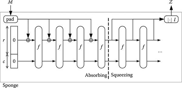
FIGURE 16.4 Sponge function.
Table 16.1 Performance of SHA 3
Area (kGE) |
Energy (mJ/Gbit) |
Throughput (Gbps) |
Clock Frequency (mHz) |
Clock Frequency for 20 Gbps Throughput |
50 |
2.42 |
43.011 |
949 |
441 |
In Henzen et al. [26], an ASIC hardware implementation of SHA-3 hash standard is given. The authors first developed a golden model and then used it to generate the stimuli vectors and expected responses to verify the register-transfer level (RTL) description of the algorithm written in Very high speed integrated circuit Hardware Description Language. They then used Synopsys Design Vision-2009.06 to map the RTL description to the UMC 90-nm technology using the fsd0a_a_2009Q2v2.0 RVT standard cell library from the Faraday Technology Corporation. All outputs are assumed to have a capacitive loading of 50 fF, and the input drive strength is assumed to be that of a medium strength buffer.
Postlayout performances of SHA-3 (Keccak-256) algorithms for a target throughput of 20 Gbps in the UMC 90-nm process as reported by Henzen et al. [26] are given in Table 16.1.
16.9 Conclusion
In this chapter, we discussed VLSI implementations of various cryptographic primitives such as stream ciphers, block ciphers, public-key ciphers, and hash functions. We included the brief descriptions of some of the major hardware implementations of these algorithms. There is a lack of standard among various implementations. With the advancement of hardware technologies, we hope that faster and efficient implementations of the cryptographic algorithms can be carried out on handheld devices.
References
1. IEEE Standard Specifications for Public-Key Cryptography, IEEE P1363, January 2000.
2. N. Koblitz, “Elliptic Curve Cryptosystems,” Mathematics of Computation, 48: 203–209, 1987.
3. K. H. Ko, J. W. Lee, T. Thomas, “Towards generating secure keys for braid cryptography,” Design Codes and Cryptography, 45(3): 317–333, 2007.
4. T. Thomas, A. K. Lal, “A zero-knowledge undeniable signature scheme in non-abelian group setting,” Int. J. Net. Sec., 6(3): 265–269, 2008.
5. P. Kitsos, G. Kostopoulos, N. Sklavos, O. Koufopavlou, “Hardware implementation of the RC4 stream cipher,” IEEE 46th Midwest Symposium on Circuits and Systems, 3: 1363–1366, 2003.
6. Data Encryption Standard (DES). Fed. Inf. Process. Standards Pub, FIPS 46-3, October 1999.
7. P. Kitsos, S. Goudevenos, O. Koufopavlou, “VLSI implementations of the triple-DES block cipher,” Proceedings of the 10th IEEE International Conference on Electronics, Circuits and Systems, ICECS 2003.
8. Advanced Encryption Standard (AES). Fed. Inf. Process. Standards Pub, FIPS 197, November 2001.
9. X. Zhang, K. K. Parhi, “High-speed VLSI architectures for the AES algorithm,” IEEE Transactions on Very Large Scale Integration (VLSI) Systems, 12(9), September 2004.
10. A. Satoh, S. Morioka, K. Takano, S. Munetoh, “A compact Rijndael hardware architecture with S-Box optimization,” in Proc. ASIACRYPT 2001, Gold Coast, Australia, pp. 239–254, December 2000.
11. A. Rudra, P. K. Dubey, C. S. Jutla, V. Kumar, J. R. Rao, P. Rohatgi, “Efficient implementation of Rijndael encryption with composite field arithmetic,” Proc. CHES 2001, Paris, France, pp. 171–184, May 2001.
12. Y. Eslami, A. Sheikholeslami, P. G. Gulak, S. Masui, K. Mukaida, “An area-efficient universal cryptography processor for smart cards,” IEEE Transactions on Very Large Scale Integration (VLSI) Systems, 14(1): 43–56, January 2006.
13. S. E. Eldridge, D. Walter, “Hardware implementation of Montgomerys modular multiplication algorithm,” IEEE Trans. Comput., 42: 693–699, June 1993.
14. C. K. Koc, C. Y. Hung, “Bit-level systolic arrays for modular multiplication,” J. VLSI Sig. Proc., 3: 215–223, 1991.
15. A. Vandemeulebroecke, E. Vanzieleghem, T. Denayer, P. G. A. Jespers, “A new carry-free division algorithm and its application to a single chip 1024-b RSA processor,” IEEE J. Solid-State Circuits, 25: 748–755, June 1990.
16. C. D. Walter, “Systolic modular multiplication,” IEEE Trans. Comput., 42: 376–378, March 1993.
17. G. R. Blakley, “A computer algorithm for the product AB modulo M,” IEEE Trans. Comput., 32: 497500, 1983.
18. Y. J. Jeong, W. P. Burleson, “VLSI array algorithms and architectures for RSA modular multiplication,” IEEE Transactions on Very Large Scale Integration (VLSI) Systems, 5(2): 211–217, June 1997.
19. P. L. Montgomery, “Modular multiplication without trial division,” Math. Comp., 44: 519–521, 1985.
20. V. S. Miller, “Use of elliptic curves in cryptography,” In Advances in Cryptology - CRYPTO 85, Springer-Verlag, Santa Barbara, CA, August 18–22, 1985.
21. E. Wenger, M. Hutter, “Exploring the design space of prime field vs. binary field ECC-hardware implementations,” Information Security Technology for Applications, Lecture Notes in Computer Science, 7161: 256–271 2012.
22. National Institute of Standards and Technology, “Announcing request for candidate algorithm nominations for a new cryptographic hash algorithm (SHA-3) family.” Federal Register, 72(212): 62212–62220, 2007.
23. C. D. Canniere, C. Rechberger, “Finding SHA-1 characteristics: General results and applications,” In Advances in Cryptology - ASIACRYPT 2006, vol 4284 of LNCS, p. 120. Springer, Berlin, Germany, 2006.
24. C. D. Canniere, C. Rechberger, “Preimages for reduced SHA-0 and SHA-1,” In Advances in Cryptology - CRYPTO 2008, vol 5157 of LNCS, pp. 179–202. Springer, Berlin, Germany, 2008.
25. X. Wang, H. Yu, “How to break MD5 and other hash functions,” In Advances in Cryptology - EUROCRYPT 2005, vol 3494 of LNCS, p. 1935. Springer, Berlin/Heidelberg, Germany, 2005.
26. L. Henzen, P. Gendotti, P. Guillet, E. Pargaetzi, M. Zoller, F. K. Gurkaynak, “Developing a hardware evaluation method for SHA-3 candidates,” Cryptographic Hardware and Embedded Systems, CHES 2010, Lecture Notes in Computer Science, 6225: 248–263, 2010.