
3 Novel Capacitor-Less A2RAM Memory Cells for Beyond 22-nm Nodes
Noel Rodríguez and Francisco Gamiz
Contents
3.2 Multibody Floating-Body-1T-Dynamic Random-Access Memory
3.3 A2RAM Memory Concept and Fabrication
3.4 Experimental Electrical Results
3.5 Tridimensional A2RAM: FinFET, Tri-Gate, and Nanowire A2RAM
3.1 Introduction
The semiconductor industry is facing a period where the survival of mature technologies is being questioned. Short-channel effects, leakage, and variability are suited as insurmountable obstacles that standard metal–oxide–semiconductor field-effect transistor (MOSFET) would not be able to overcome in the ultimate nodes. In the case of the memory field, the situation is analogous. Mainstream technologies (Flash, static random-access memory [SRAM], dynamic random-access memory [DRAM]) are threatened by particular issues related to their scalability.1 In parallel new emerging alternatives, that is, resistive random-access memory, magnetoresistive random-access memory, floating-body DRAMs (FB-DRAMs), and so on, are claiming to solve the issues of the established technologies.
FB-DRAMs are one of the candidates positioned for SRAM/DRAM replacement. In this approach, the isolated body of a silicon-on-insulator (SOI) transistor is used to store charge that changes the electrical potential of the transistor and therefore the way it drives the current. This approach has a long way back since the first works suggesting the application of SOI-MOSFET as single-transistor memory cells were made back in the 1990s when Kuo et al.2 anticipated the current flow modulation in fully depleted SOI transistor by modifying the charge at the opposite interface.2 However, it was at the beginning of the new century when the floating-body memory cell became a subject of intense research. Since then, there have been multiple proposals combining different methods to store the charge in the body of the transistor and different ways to sense the state of the cell from simple MOSFET operation to bipolar current breakdown.3–7 Each particular approach has its own advantages and drawbacks, but none of them has risen yet as competitive opponent to the standard technologies. The search of a charge-based cell, substitute of DRAMs, has continued evolving during the last years, bearing encouraging fruits as novel thyristor-like structures or multibody cells giving another twist to the subject.8,9 In this chapter we will focus in one of the particular approaches pointed out as fast storage (SRAM, DRAM) substitute: the recently introduced floating-body A2RAM cell.
3.2 Multibody Floating-Body-1T-Dynamic Random-Access Memory
One of the trends followed by the FB-DRAM researches lies in the modification of the body of the transistor to create multibody structures defining dedicated regions for the charge storage and the current flow. The basics for introducing this complexity in the device arise from scalability constrains.10 FB-DRAM cells are intrinsically very dependent on SOI technology. The scaling of the gate length of an SOI transistor requires for the simultaneous scaling of the silicon film thickness.11 This condition introduces a paramount challenge: how to allow the simultaneous coexistence of holes (which represent the information in terms of charge) and electrons (which are the carriers involved in the current flow for discriminating the state in the device) in the same ultrathin silicon film. The solution to surmount this limitation implies innovative solutions enhancing the electrostatic potential differences that the body of the transistor can sustain. One possibility is to create specific regions (or bodies) to store the holes. Figure 3.1 shows three variants of multibody floating-body cells. In Figure 3.1a, a schematic of the single-transistor quantum well (QW) 1T-DRAM is presented.12 This device is based on an engineered-body material that integrates, within the Si film, a thin layer of a material with a lower bandgap (i.e., SiGe). This last layer creates an electrostatic-potential well for storage of holes. It was theoretically demonstrated that this structure improves the current sensing margin and scalability characteristics. As the QW devices are more scalable, thanks to the introduction of a “more efficient storage room,” the effect of the volume reduction with the channel length is mitigated.
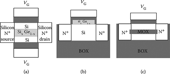
FIGURE 3.1 Schematic examples of multibody floating-body dynamic random-access memory cells. (a) Quantum well floating-body dynamic random-access memory: the holes are stored in a potential well created by the Si–Ge layer.11 (b) Convex channel 1T-dynamic random-access memory: the holes are stored in a Si–Ge layer created into the gate stack.12 (c) A-RAM memory cell: the body of the transistor is partitioned in two dedicated regions for hole storage and electron current sensing.13 The bodies are separated by a low-k dielectric layer. This layer provides the electrostatic potential difference needed for electron–hole coexistence.
The second example of multibody FB-DRAM cell is the convex channel 1T-DRAM structure (Figure 3.1b), which using the bipolar junction transistor (BJT) programming technique, was proposed to improve the retention time.13 Holes are stored beneath a raised gate oxide that may be filled by a smaller bandgap material (e.g., SiGe) (Figure 3.1b). As the holes stored during the “1” state programming reduce the body/source (drain) potential barrier, they easily diffuse through these junctions filling the SiGe region. The convex channel architecture provides a physical well for more effective storage of holes. Moreover, if a narrower bandgap material is used in the convex channel region, a deeper potential well is formed improving further the sensing margin and retention time.
Finally, the last example proposes the physical partitioning of the body of the transistor into two isolated regions (Figure 3.1c) by a middle oxide (MOX).14 To take advantage of this structure, the MOX must have a dielectric constant smaller than silicon, for example, SiO2. The resulting semibodies share the source and drain regions of the transistor. When this device is operated as a memory cell, the top semibody is used for majority carrier storage (holes) accommodated in a potential well created by the negative bias of the gate. The bottom semibody serves to sense the cell state via the minority carrier current. The low-k MOX constitutes the key advantage of this device: the electrostatic potential difference between the front and back interfaces is enlarged due to a higher electrostatic potential drop through the MOX.
3.3 A2Ram Memory Concept and Fabrication
The second generation of the A-RAM cell or A2RAM, the main subject of this chapter, lays the foundations of a doping-based partitioning of the body of the transistor.15 The device is a regular MOSFET with a retrograde N–P doping profile starting from the bottom of the body. The source and drain regions become electrically short-circuited due to the highly doped bottom region (named N-bridge) (Figure 3.2). The memory states are defined by the conductivity level of the N-bridge. A negative gate bias is applied to create a potential well for the storage of the holes (“1” state) (Figure 3.2b). Under these circumstances, the electric field induced by the gate is screened by the positive charge of the P-type body (accumulated holes), and the electron concentration in the N-bridge (majority carriers) remains high. Biasing the drain, which is the way to easily test the state of the cell, makes an electron current to flow from source to drain through the N-bridge. In the “0” state, the holes are evacuated from the upper P-body: the gate electric field is no longer screened affecting the population of electrons of the N-bridge. If the device is well engineered, the N-bridge will become fully depleted during “0” state leading to a very low current flow, and therefore, a large margin between states (Figure 3.2c). One of the main advantages of this concept is that the use of an insulator substrate is not mandatory: the holes are stored in the potential well created at the top interface, and the electrons are confined by the N-bridge. There is no need for a physical insulator barrier at the back interface or a back-gate bias.
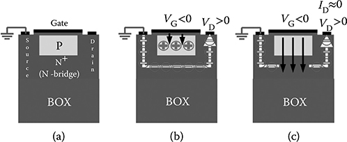
FIGURE 3.2 A2RAM memory cell: (a) The source and drain of a regular metal–oxide–semiconductor field-effect transistor are short-circuited by a buried N-type layer.14 (b) In “1” state, the top body of the cell is charged with holes that screen the gate electric field allowing the current flow from source to drain through the highly doped N-bridge. (c) In “0” state, the top body is depleted of charge; the gate electric field is not screened; the N-bridge is fully depleted avoiding the current flow.
Prototypes of A2RAM cells have been fabricated in different technologies including 2.5-µm SOI, 2.5-µm bulk, and 22-nm SOI.16 These devices were used as initial demonstrators for the viability of the concept, initially only supported by numerical simulations.15 Figure 3.3a shows a transmission electron microscopy image of one of these prototypes fabricated in the more challenging 22-nm technology.16 The fabrication adds two additional steps to the standard complementary metal–oxide–semiconductor (CMOS) process (Figure 3.3b). First, an arsenic implantation to introduce the N-type dopants for the N-bridge; second, a selective epitaxial growth (SEG) to generate the characteristic N–P retrograde doping profile establishing the body partitioning. Figure 3.3c shows results from ATHENA process simulations on the final vertical net doping profile of the device after the entire thermal load. It can be observed that the final profile achieves the bottom highly doped N-type layer under the low-doped P-type layer in a 36-nm thick body.
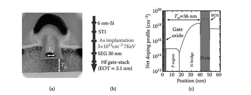
FIGURE 3.3 (a) Transmission electron microscopy image of an A2RAM memory cell fabricated on a 22-nm silicon-on-insulator process at CEA-LETI facilities.15 (b) Simplified process flow: the key steps allowing the formation of the N-bridge are the implantation of the arsenic ions followed by a selective epitaxial growth. (c) Simulated resulting doping profile of the fabricated device after the entire thermal load.
It is worth noting that if the required maximum thickness limit for the silicon film can be relaxed, the process flow can be further simplified avoiding the SEG step. This could be interesting for nonultimate embedded memory applications with longer channels and consequently thicker silicon films.
A proper calibration of the doping of the N-bridge is necessary to ensure a large margin between states. Figure 3.4 shows an example of the target doping level for the N-bridge considering a device with a gate length of L = 100 nm. For a given N-bridge doping, if the bridge is too thick, the device will have large leakage in the “0” state becoming very difficult to fully deplete the N-doped layer with reasonable gate bias. In contrast, if the bridge is too thin, it will be fully depleted even in the “1” state by the action of the negative gate bias during holding and reading, leading to a very low “1” state current. In our fabricated prototype cells, the N-bridge thickness is around 22 nm and the average doping approximately 2 × 1017 cm−3, therefore they are in the target area.
3.4 Experimental Electrical Results
The clearest evidence of the viability of the A2RAM concept as memory cell is manifested when the device is biased with a pulse pattern emulating the actual memory operation of the device in a matrix. The voltage waveform is generated with an arbitrary function generator with the capability to measure in real time the driven current.17 The bias sequence (Figure 3.5a) starts with a positive drain-bias pulse overlapped with a negative gate-bias pulse. The large electric field created in the drain-to-gate overlap region allows the injection of holes by band-to-band (BTB) tunneling.15 The large concentration of holes after the W“1” pulse screens the electric field induced by the negative bias of the gate taking the N-bridge to its conductive state. Note that there is a peak of current during the W“1” event. This current is generated by the electron flow through the N-bridge due to the large drain bias during the writing process (see Figure 3.5b). When the hole concentration starts to be substantial, the N-bridge passes from a full-depletion situation to a partial-depletion situation presenting an increasing conductivity. A proper calibration of the width and level of the voltage pulses is necessary to avoid an excessive drain current during a W“1” event. This depends on the size of the cell.
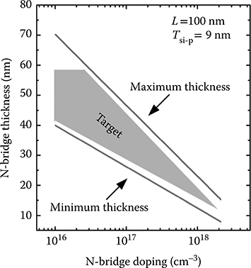
FIGURE 3.4 Maximum and minimum thickness of the N-bridge depending on its doping (assumed constant) to achieve a current ratio between the “1” and “0” state over 100 in an L = 100 nm with P-type body of 9 nm.
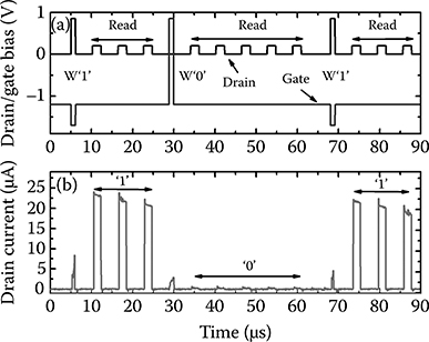
FIGURE 3.5 Experimental measurements of the drain current of an A2RAM memory cell with gate length L = 100 nm. (a) The voltage pattern for the test is applied to the drain and gate terminals. The sequence is as follows: write “1,” read three times, write “0,” read five times, write “1,” and read three times (b) Drain current readout.
After the W“1” event, the state of the cell is read three times. This is simply achieved by slightly increasing the drain bias to test whether the bridge is in a conductive condition or not. As observed, three pulses of current are immediately obtained in the drain corresponding to a conductive bridge situation. It is noticeable that the read current shows a decay with time. This is due to the overpopulation of holes in the body produced during the W“1” event. Actually, under the bias conditions used, the number of holes injected in the body is larger than the concentration that can be sustained by the gate bias corresponding to the thermodynamic equilibrium. The excess of holes gradually recombines leading to a slight current decrease until the equilibrium condition.
In the next step, a writing “0” event (W“0”) is applied to the device (timê30 μs). The bias conditions necessary to fully deplete the N-bridge are simply a positive voltage pulse in the gate. The sudden increase in the body potential forward biases the body-to-source and body-to-drain junctions evacuating the holes from the upper body of the transistor through these junctions. Because the body potential decreases quickly (as the gate bias return to a negative value), the body of the transistor enters in a deep-depletion condition.
The state of the cell is read five times by increasing the drain bias leading to negligible current in this axis scale. The difference with the previous current levels (“1” state) is enough to discriminate clearly the state of the device. More results on the current ratio between “1” and “0” states are presented in Figure 3.6. The ratio is shown against the gate length of the device. For the batch of A2RAM cells fabricated, the maximum ratio occurs at L ~ 100 nm. This result was expected because the devices were optimized for that gate length. As the gate length decreases below 100 nm, so does the current ratio because it becomes more difficult to fully deplete the N-bridge during the “0” state (for further scaling of the device length, it is necessary to reduce the doping level).
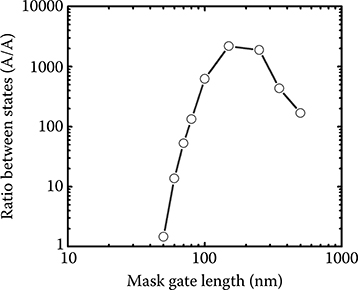
FIGURE 3.6 Current ratio between “1” and “0” states as a function of the channel length in A2RAM prototypes.
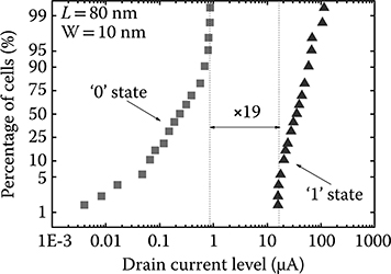
FIGURE 3.7 Statistical cumulative plots of the current levels in the “1” (triangles) and “0” (squares) 1 μs after the witting events. It is worth noting that the distribution never overlaps presenting a safety guard factor of 19.
Despite the A2RAM, devices fabricated up to now have been purely experimental demonstrators; it is interesting to show the variability of the prototyped devices. Figure 3.7 presents statistical results on the “1” and “0” current levels 10 μs after the writing events. The average current margin is about two orders of magnitude. For this particular dimensions, the maximum current in the “0” state is below 1 μA, whereas the minimum current in the “1” state is above 10 μA. The actual safety guard margin is a factor of 19.
As in any other FB-DRAM cell, in the A2RAM structure, the current margin between states does not prevail indefinitely. The parasitic BTB tunneling during the holding phase of the operation restores the hole population in the P-type body turning the “0” state into “1” state. The retention time is defined as the time required for the “0” state to recover half of the current corresponding to the stable “1” state. Results for different FB-DRAM flavors are shown in Figure 3.8. A2RAM presents very competitive retention time (average 3 ms at 85°C and 10 ms at 25°C) compared even with less scaled multigate structures.18 The so-called bipolar Z-RAM establishes the reference, but at the expense of much larger voltages when is operated (which ultimately introduce disturbance and reliability concerns).
We would like to finish this section by considering a very important aspect that needs to be validated for any novel technology that intends to have an industrial application. The immunity to disturbance effects is one of the main challenges of any memory technology and an issue of especial relevance in the case of floating-body memories. A disturbance event can be considered a change in the bias lines of a memory matrix that may change unintentionally the state of a cell in holding state while accessing a different cell for reading or writing. In the case of the A2RAM memory, the disturbance events can affect the “0” unstable state; the “1” state cannot be turned into “0” state by the bias pattern proposed for the operation of the device (Figure 3.5). There are two cases where the “0” state may be disturbed, represented in Figures 3.9 and 3.10, depending if the change in the bias line occurs at the gate terminal or at the drain terminal.
Figure 3.9a represents a very simplistic memory matrix of A2RAM cells (three words of three bits). The little triangle at the drain of the devices represents the cell selector that controls the current flow of the cell (this device could be a diode or a transistor in an actual implementation). We are going to consider the disturbance situation of the cell (“disturbed cell,” indicated with a lighting in Figure 3.9a) when we write a “1” state in the next cell sharing the drain and gate lines (“target cell,” closed into the dashed line in Figure 3.9a). To write the “1” state in the target cell, it is necessary to decrease the gate bias and increase the source bias (acting as drain in this case) to trigger the BTB tunneling injection of holes. Meanwhile, the disturbed cell is holding a “0” state and may suffer from a decrease in the gate voltage that may trigger also the BTB tunneling injection of holes, turning the “0” state into “1” state. The situation previously described has been emulated in Figure 3.9b. Initially we write the “1” state to an isolated A2RAM transistor and we read the driven current. Next we write a “0” state and read it consecutively. In between each reading drain pulse, we apply a negative gate voltage pulse over the holding bias, what emulates the disturbance condition described in Figure 3.9a. As observed, the disturbance of the gate does not modify the “0” state.
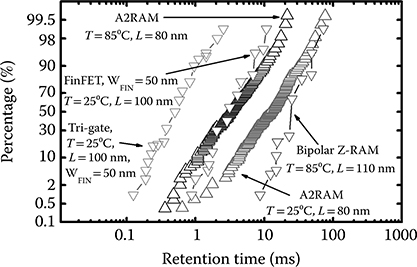
FIGURE 3.8 Statistical cumulative plots of the retention time are 25°C and 85°C compared with other floating-body-dynamic random-access memories.
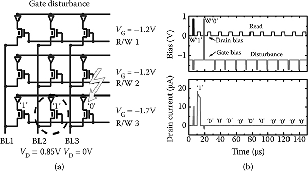
FIGURE 3.9 (a) Schematic of a simplistic A2RAM three words/three bits memory matrix to study gate disturbance phenomenon. The role of source and drain terminal is exchanged depending on the bias. (b) Experimental measurements of the current read in the “0” state during sequential reading with gate disturbance events in between them.
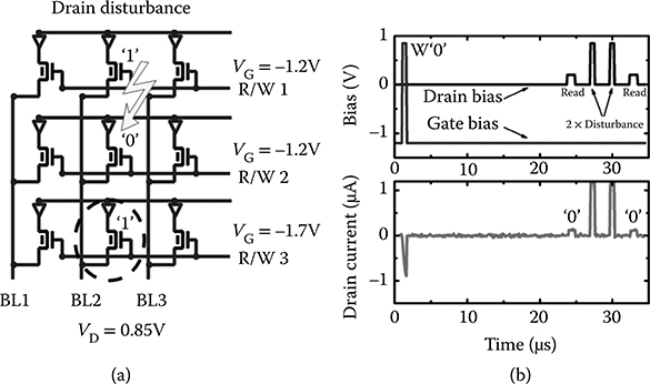
FIGURE 3.10 (a) Schematic of a simplistic A2RAM three words/three bits memory matrix to study drain disturbance phenomenon. The role of source and drain terminal is exchanged depending on the bias. (b) Experimental measurements of the current read in the “0” state before and after two drain disturbance events.
The other possibility of disturbance happens when a target cell in which the “1” state must be stored (target cell, marked in dashed line in Figure 3.10a) is sharing the drain line with a cell which is holding the “0” state (disturbed cell, cell indicated with the lighting in Figure 3.10a). The increase in the source bias (acting as drain in this case) may trigger the BTB tunneling in the disturbed cell. Figure 3.10b shows the experimental conditions of this event in a single isolated device. Initially, the “0” state is written by pulsing the gate voltage. Next, the current is read by slightly increasing the drain bias, then the cell is disturbed by the applying higher voltage pulses to the drain twice and, finally the cell is read again. As observed, the current of the “0” state after the disturbance does not present any change as compared to the current of the “0” state before the disturbance.
Summarizing, we can affirm that the waveform pattern developed for the operation of this experimental A2RAM memory cell makes them also immune to disturbance events during the writing and reading processes. Only the simultaneous decrease of the gate bias and increase in the drain bias can trigger the BTB tunneling injection to turn a “0” state into a “1” state. As mentioned previously, immunity to disturbance is a paramount challenge for any solid-state storage technology and especially for floating-body based cells.
3.5 Tridimensional A2Ram: Finfet, Tri-Gate, and Nanowire A2Ram
Several foundries (Intel among others) have recently introduced 3D Tri-Gate transistors in their 22-nm nodes, that is, three gates wrapped around the silicon channel in a 3D structure.19 These transistors are expected to provide ultralow power benefits for use in portable devices, like smartphones and tablets, while also delivering improved performance normally expected for high-end processors. The concept of multibody partitioning 1T-DRAM cells, demonstrated previously in planar devices, can be also transferred to 3D structures (FinFET, Tri-Gate, and nanowire transistors), thus enabling memory cells with low voltage operation, energy efficiency, high performance, and fabrication compatibility as embedded memory in next technological nodes. A 3D picture of the proposed memory cell, on SOI substrate, is shown in Figure 3.11. Doping sections from source to drain and perpendicular to the BOX are shown in Figure 3.12. As observed, a conventional triple-gate field-effect transistor (FET) is modified by connecting the N+ source and drain through an inner N-type wire (Figure 3.11). Typical total Fin width can vary from 15 to 25 nm.
The doping profiles have been generated by process simulator ATHENA, thus validating the device feasibility. The 14-nm-thick core N-bridge is 5 × 1018 cm−3 doped, whereas the surrounding 4-nm P-type body is maintained undoped (NA = 1014 cm−3 residual boron) (Figure 3.12). The P-type external crust that surrounds the N-type core is used as the storage node while the internal core (high doped N-bridge) is used for current sense (Figure 3.12a).
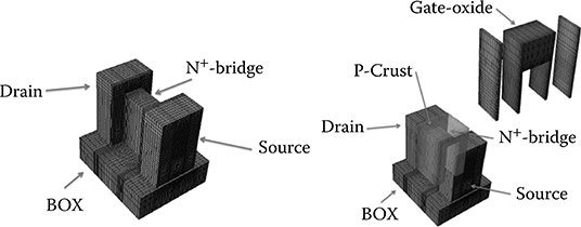
FIGURE 3.11 Schematic representation of the 3D A2RAM memory cell.
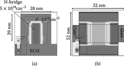
FIGURE 3.12 (a) Doping cross-section (perpendicular to the BOX, parallel to source and drain) of the Triple-gate A2RAM. The high-doped N-bridge (5 × 1018 cm−3) short-circuiting source and drain is surrounded by a low-doped P-type layer (1014 cm−3). (b) 2D-doping cross-section (parallel to the BOX) of the triple-gate A2RAM. The gate is 3 nm underlapped to improve retention characteristics.
The memory effect relies on the same principle as planar A2RAM cell explained in Section 3.3: when the P-type crust is charged with holes (generated by BTB tunneling and retained with a negative gate bias), the gate electric field is screened by the accumulation layer and cannot deplete the N-bridge. If VD is increased, an electron current flows through the neutral region of the N-bridge, which behaves as a simple resistor (state “1”). The current flow through the P-body is negligible (reverse-biased junctions). When the outer P crust is empty of holes, the gate field is no longer screened and fully depletes the N-bridge: the drain current becomes extremely low (“0” state). As in planar A2RAM, differences with conventional 1T-DRAMs are twofold: (1) the drain current (defining the cell state) is due to majority carriers flowing in the volume of the bridge, (2) the coexistence of holes and electrons is ensured by the P/N junction (supercoupling suppression).
The combination of the P and N channels results in unconventional ID–VG characteristics. We have used numerical simulations to demonstrate the functionality as memory cell of the 3D A2RAM device; Poisson and continuity equations were solved self-consistently in 3D. First, we studied the steady state operation of the cell (continuous section of drain current curve in Figure 3.13): the combination of the parallel P and N channels results in unconventional ID–VG curves. In steady state, the N-bridge is always nondepleted regardless of the gate voltage. For negative VG, the potential difference is basically absorbed by the accumulated holes in the crust P region: the more negative the gate voltage, the more holes accumulate, screening the electric field, and the drain current, which is mainly limited by the conductivity of the N+-core acting as a resistor, is weakly dependent on VG. On the contrary, for positive gate bias, the current flow comes from the parallel combination of the majority carriers (electrons) of the N-bridge (which behaves like a resistor), and the minority carriers (electrons) of the top MOSFET. As the gate bias is increased, the top inversion channel becomes dominant. Notice that this behavior is different from that of a depletion-mode NMOSFET, where the conduction can be effectively cut at a certain negative gate bias.
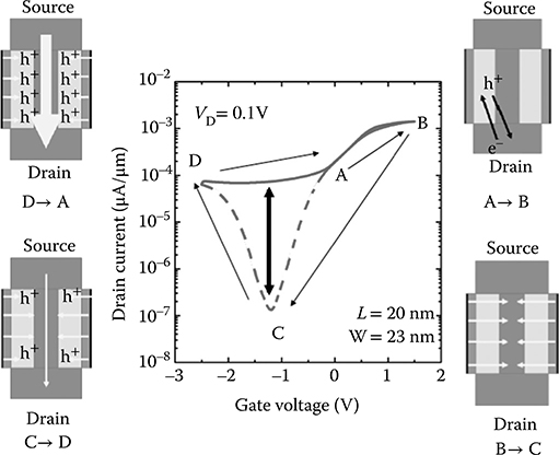
FIGURE 3.13 Hysteresis curve demonstrating the memory effect obtained by looping the gate voltage between 1.5 and −2.5 V.
The transient behavior is analyzed in Figure 3.13:
From A to B, a positive voltage is applied to the gate. The upper channel becomes inverted with electrons, and the behavior of the device is similar to that of a MOSFET transistor.
From B to C, a negative voltage is suddenly applied to the gate. The channel becomes depleted of electrons, and as there are no sources of holes, the upper channel becomes empty of carriers. The negative electric field induced by the negative gate voltage also depletes the N-bridge and as a consequence, there is no current at all in the device.
If the gate voltage is decreased to even more negative values (C to D), BTB tunneling starts to appear in the source-channel and drain-channel overlapped regions. This process injects holes into the channel that screens the negative electric field induced by the gate. As the negative gate electric field is now weaker, the N-bridge becomes partially undepleted and the drain current starts to increase. The greater the hole injection, the higher the drain current.
If the gate voltage is reduced to zero (D to A), BTB tunneling stops, no more holes are injected in the channel and the drain current becomes constant.
As observed in Figure 3.13, under negative gate voltages, there is a current window for the same values of gate and drain voltages, which, depending on the population of holes in the upper channel, allows the definition of two memory states:
“1” state: Upper channel is populated with holes that screen the negative electric field. Drain current flows through the buried N-bridge.
“0” state: Upper channel is in deep-depletion of carriers. The negative electric field induced by the negative gate voltage depletes the N-bridge, and no current flows between drain and source. This state is nonequilibrium state. After a long time, thermal carrier generation, junction leakage, and BTB tunneling will restore the hole population in the channel, and the “0” state will be corrupted.
Figure 3.14 shows the memory operation. The gate is biased below the threshold voltage to accommodate an accumulation of holes in the channel, which will define the “1” state current. Initially, the cell is purged by writing “0” state with a positive gate-voltage pulse. Because the pulse forward-biases the channel-source and channel-drain P–N junctions, the holes are expelled from the channel. When the gate returns to the negative holding bias, there are no carriers in the channel.
We propose two alternative mechanisms to write the “1” states (restore the hole population in the P-body): BTB tunneling by means of an over-bias pulse of the retention gate voltage, or impact ionization by applying a positive gate voltage in the gate activating the MOSFET. Nevertheless, BTB tunneling is best suited for low-power embedded applications because the writing current is typically several orders of magnitude lower than with the impact ionization mechanism (during the writing time, there is an additional contribution of current coming from the MOSFET, which is not present when using the BTB mechanism). Waveforms demonstrating the cell functionality are shown in Figure 3.14 using the BTB alternative. As observed, the “0” state virtually corresponds to zero drain current.
The potential scalability of A2RAM and its expansion to nonplanar devices gain evidence with the previous simulations. Further research and optimized prototypes may position this device in the backstage of the memory scenario waiting for a commercial application.
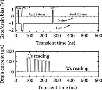
FIGURE 3.14 Full 1T dynamic random-access memory operation of a 3D-A2RAM cell. Top: Drain and gate bias pattern. The cell is initially purged (W0), then the “1” state is written by band-to-band tunneling and read eight times. Next the “0” state is written by purging again the cell and read 12 times. Bottom: Drain current reading.
3.6 Conclusions
We would like to conclude this chapter with a set of open questions that summarizes the outcome of the results presented along the previous pages.
Is a charge-based bit the best fundamental of a memory cell? If we think in terms of scalability, the common sense immediate answer will be no. The stored charge will scale down with the dimensions of the cell, therefore leading to poor sensitivity, larger variability, and easier disturbance among other issues. Material-property-based memories as magnetic RAMs or resistive RAMs may behave better under a very aggressive scaling scenario. This can be considered a paradoxical situation, because in the origins of the automatic treatment of stored information, the memory modules were also material based from simple punched cards to more advanced magnetics tape. So, is the memory industry going back to a nanoscaled version of its origins? Considering that the standard CMOS process is the milestone of the digital world, the answer, thinking in terms of embedded memory, turns more complicated. Introducing new materials with delicate thermal properties is something that the semiconductor industry will not be graceful to afford. Despite in every technology node, the continuity of standard DRAM cells has been questioned, the industry keeps pushing the limits of this 40-year-old technology. In this context, what is the destiny of A2RAM and its floating-body counterparts? It has been probed that A2RAM is a reality; it performs well in all the aspect studied, and considering the overall concept, it can outperform most of its floating-body counterparts. However, a change in paradigm means more than a substitution of the single DRAM cell, but a complete redesign of the memory scheme starting from the memory matrix. This is therefore something utopic as far as standard DRAM has demonstrated its scalability up to now, and probably it will continue doing so in the next node at the expense of a higher cost and complexity. A2RAM may target specific applications with need of cheap embedded storage (maybe not ultimately scaled) where it can considerably simplify the fabrication process. The last word will come from the semiconductor industry and its need from design innovation and cost reduction.
References
1. K. Kim. Perspectives on giga-bit scaled DRAM technology generation, Microelectronics Reliability 40(2): 191–206, 2000.
2. F. A. Eraghi, J. Chen, R. Solomon, T. Chan, P. Ko, and C. Hu. Time dependence of fully depleted SOI MOSFET’s subthreshold current, Proceedings IEEE International SOI Conference, Vail Vally, CO, 32–33, October 1991.
3. S. Okhonin, M. Nagoga, J. M. Sallese, and P. Fazan. A capacitor-less 1T-DRAM cell, IEEE Electron Device Letters, 23(2): 85–87, February 2002.
4. C. Kuo, T. J. King, and C. Hu. A capacitorless double-gate DRAM cell, IEEE Electron Device Letters, 23(6): 345–347, June 2002.
5. S. Okhonin, M. Nagoga, E. Carman, R. Beffa, and E. Faraoni. New generation of Z-RAM, IEEE International Electron Devices Meeting, Washington, DC, 925–928, 2007.
6. K. W. Song, H. Jeong, J. W. Lee, S. I. Hong, N. K. Tak, Y. T. Kim, Y. L. Choi et al. 55 nm capacitor-less 1T DRAM cell transistor with non-overlap structure, Electron Devices Meeting in IEDM Technical Digest, San Francisco, CA, 1–4, December 2008.
7. Z. Lu, N. Collaert, M. Aoulaiche, B. De Wachter, A. De Keersgieter, W. Schwarzenbach, O. Bonnin et al. A novel low-voltage biasing scheme for double gate FBC achieving 5s retention and 1016 endurance at 85°C, Electron Devices Meeting (IEDM), 2010 IEEE International, San Francisco, CA, 12.3.1–12.3.4., 2010.
8. Y. K. J. Yang, R. N. Gupta, S. Banna, F. Nemati, H. J. Cho, M. Ershov, M. Tarabbia, D. Hayes, and S. T. Robins. Optimization of nanoscale thyristor on SOI for high-performance high-density memories, IEEE International SOI Conference, Niagara Falls, New York, 113–114, 2006.
9. J. Wan, C. Le Royer, A. Zaslavsky, and S. Cristoloveanu. A compact capacitor-less high-speed DRAM using field effect-controlled charge regeneration, IEEE Electron Device Letters, 33(2): 179–181, 2012.
10. T. Hamamoto. Overview and future challenges of floating body RAM (FBRAM) technology for 32 nm technology node and beyond, Proceedings Solid-State Device Research Conference, Edinburgh, Scotland, 25–29, 2008.
11. J. P. Colinge. Silicon-On-Insulator Technology: Materials to VLSI, 3rd ed. Kluwer Academic Publishers, Dordrecht, The Netherlands, 2004.
12. M. Ertosun, P. Kapur, and K. Saraswat. A highly scalable capacitorless double gate quantum well single transistor DRAM: 1T-QW DRAM, IEEE Electron Device Letters, 29: 1405–1407, 2008.
13. M. Cho, C. Shin, and T. Liu. Convex channel design for improved capacitorless DRAM retention time, International Conference on Simulation of Semiconductor Processes and Devices, SISPAD, San Diego, CA, 1–4, 2009.
14. N. Rodriguez, F. Gamiz, and S. Cristoloveanu. A-RAM memory cell: Concept and operation, IEEE Electron Device Letters, 31(9): 972–974, 2010.
15. N. Rodriguez, S. Cristoloveanu, and F. Gamiz. Novel capacitorless 1T-DRAM cell for 22-nm node compatible with bulk and SOI substrates, IEEE Transactions on Electron Devices, 58(8): 2371–2377, August 2011.
16. N. Rodriguez, C. Navarro, F. Gamiz, F. Andrieu, O. Faynot, and S. Cristoloveanu. Experimental demonstration of capacitorless A2RAM cells on silicon-on-insulator, IEEE Electron Device Letters, 33(12): 1717–1719, December 2012.
17. Agilent Technologies. Agilent B1530 User Manual, 5th edition, August 2012.
18. C. Bassin, P. Fazan, W. Xiong, C. Cleavelin, T. Schulz, K. Schruefer, M. Gostkowski et al. Retention characteristics of zero-capacitor RAM (Z-RAM) cell based on FinFET and tri-gate devices, Proceedings IEEE International SOI Conference, Honolulu, HI, 203–204, October 2005.
19. S. Damaraju, V. George, S. Jahagirdar, T. Khondker, R. Milstrey, S. Sarkar, S. Scott, I. Stolero, and A. Subbiah. A 22 nm IA multi-CPU and GPU system-on-chip, Solid-State Circuits Conference Digest of Technical Papers (ISSCC), 2012 IEEE International, IEEE, San Francisco, CA, 56–57, February 2012.