This chapter is about the mikroC Pro for ARM Integrated Development Environment (IDE). The IDE consists of a text editor, standard C compiler, simulator, program loader, and debugger. This chapter describes how to use the various software tools of the IDE. Configuring the clock of the STM32F407 microcontroller is a complicated task. This chapter describes in detail how the clock of the STM32F407 can be configured using the Excel-based clock configuration utility. Additionally, an example program is given in this chapter to show how a simple project can be developed for the Clicker 2 for STM32 development board, and also how the executable code can be uploaded to the program memory of the target microcontroller. Step-by-step details of using the simulator are also given using a simple program.
Keywords
mikroC Pro for ARM
IDE
GPIO library
clock configuration
digital input-output
exceptions
interrupt service routine
creating a project
simulation
breakpoints
debugging
Bootloader
library manager
output files
6.1. Overview
In the last chapter we had a look at the various Integrated Development Environments (IDEs) that can be used to program the ARM-based microcontrollers. In this book we shall be using the mikroC Pro for ARM in all the projects. This chapter describes the basic features of this IDE and gives an example project to illustrate how a program can be created, compiled, and then uploaded to the program memory of the Clicker 2 for STM32 development board. The example given in this chapter is based on the STM32F407VCT6 microcontroller since this is the processor used on the Clicker 2 for STM32 development board.
6.2. MikroC Pro for ARM
MikroC Pro for ARM (simply called mikroC from now onwards) is very similar to the standard C language but it has been developed specifically for programming ARM-based microcontrollers. mikroC allows a programmer to:
• Write source code using the built-in text editor
• Include the required library to speed up the development process
• Manage your project easily
• Monitor program structure, variables, and functions
• Generate assembly, HEX, and list files for programming the target processor
• Use the integrated simulator to debug code on your PC
• Use the integrated hardware debugger to speed up program development and testing
• Get detailed reports on memory usage, calling tree, assembly listings, and more
• Program the target processor using the integrated programming software (not available for the Clicker 2 for STM32 development board since this board is programmed using a Bootloader program).
mikroC includes libraries on hardware, digital signal processing, ANSI C, and others. Some more commonly used libraries are (there are over 60 libraries):
• ADC library
• CAN library
• EEPROM library
• Ethernet library
• GPIO library
• LCD and graphics LCD library
• Keypad library
• Sound library
• UART library
• TFT display library
• Touch panel library
• USB library
• Digital filter libraries (FIR and IIR)
• FFT library
• Matrices library
• ANSI C Math library
• Button library
• Conversions library
• Time library
• Trigonometry library
mikroC includes a built-in integrated Help facility that helps programmers to learn the format of various library statements and also to check the syntax of program statements. The advantage of this help utility is that not like the paper documentation, the help utility is up to date. mikroC organizes applications into project folders, consisting of a single project file, one or more source files, and header files, all in the same folder. The IDE helps programmers to create multiple projects. Project folders consist of the following:
• Project name
• Target microcontroller device
• Device clock
• List of project source files
• Header files
• Binary files
• Image files
• Other files
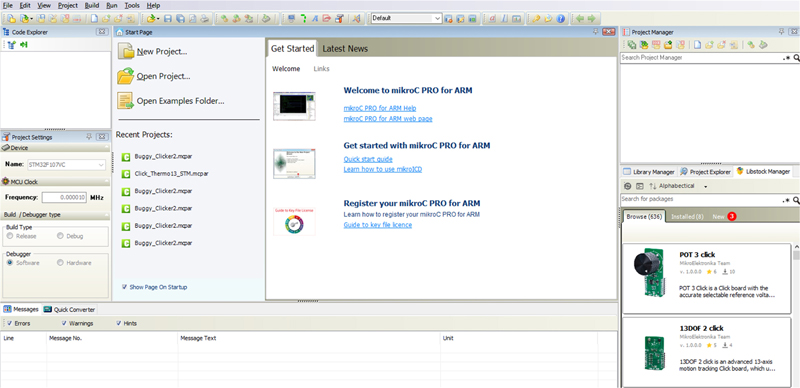
Fig. 6.1 shows the structure of a mikroC program written for the Clicker 2 for STM32 development board (as mentioned earlier, readers should note that this development board uses the STM32F407VGT6 microcontroller). Although comments are optional in a program, it is highly recommended as it makes a program easier to understand and maintain in the future. This very simple program (program: LED.c) flashes the on-board LED connected to port pin PE12 every second. We shall see in this chapter some of the STM32F407VCT6 specific features of the mikroC language. Most of the features described in this chapter are applicable to other members of the STM32 family.
Figure 6.1A simple program that flashes an LED.
People familiar with the standard C language will notice in Fig. 6.1 that there is no library include files (i.e., header files) at the beginning of the program. This is because all library files are automatically included by the compiler when a new file is created.
In the remainder of this chapter, the important GPIO library (which is used in almost all projects) and some STM32 specific features of the mikroC are described. In addition, the steps to create, compile, and upload a program to the Clicker 2 for STM32 development board are described.
6.3. The general purpose input-output library
The mikroC general purpose input-output (GPIO) library includes a set of routines for easier handling of the GPIO pin functions. The library contains the following functions (only the STM32 processor-specific features are described in this section):
• GPIO_Clk_Enable
• GPIO_Clk_Disable
• GPIO_Config
• GPIO_Set_Pin_Mode
• GPIO_Digital_Input
• GPIO_Digital_Output
• GPIO_Analog_Input
• GPIO_Alternate_Function_Enable
6.3.1. GPIO_Clk_Enable
This function enables the clock on the desired port. In the following example code, clock is enabled on PORTE:
GPIO_Clock_Enable(&GPIO_BASE)
6.3.2. GPIO_Clk_Disable
This function disables the clock on the desired port. In the following example code, clock is disabled on PORTE:
GPIO_Clock_Disable(&GPIO_BASE)
6.3.3. GPIO_Config
This function is used to configure port pins according to the parameters specified. The function has the following format:
void GPIO_Config(unsigned long *port, unsigned int pin_mask, unsigned long config)
where port is the PORT we wish to use, pin_mask is the pin we wish to configure, and config is the desired configuration of the port pin.
The function returns a 0 if there are no errors. In the following example, PORTA pins 0 and 7 are configured as digital inputs with no pull-up or pull-down resistors:
Similarly, the following example configures all pins of PORTB as digital outputs with push-pull output transistors:
GPIO_Config(&GPIOB_BASE,_GPIO_PINMASK_ALL,
_GPIO_CFG_MODE_OUTPUT |_GPIO_CFG_OTYPE_PP);
The following example configures PORTB pin 1 as digital output:
GPIO_Config(&GPIOB_BASE,_GPIO_PINMASK_1,
_GPIO_CFG_MODE_OUTPUT);
pin_mask can take the following values:
_GPIO_PINMASK_0
pin 0 mask
_GPIO_PINMASK_1
pin 1 mask
………………………………………………
_GPIO_PINMASK_15
pin 15 mask
_GPIO_PINMASK_LOW
low 8 port pins
_GPIO_PINMASK_HIGH
high 8 port pins
_GPIO_PINMASK_ALL
all pins masked
config can take different values depending upon the port usage. The following values are valid:
Basic
_GPIO_CFG_PULL_UP
configure pins as pull-up
_GPIO_CFG_PULL_DOWN
configure pins as pull-down
_GPIO_CFG_PULL_NO
configure pins as floating (no pull-up/down)
_GPIO_CFG_MODE_ALT_FUNCTION
pins have alternate functions (non GPIO)
_GPIO_CFG_MODE_ANALOG
configure pins for analog
_GPIO_CFG_OTYPE_OD
configure pins as open-drain
_GPIO_CFG_OTYPE_PP
configure pins as push-pull
_GPIO_CFG_SPEED_400KHZ
configure pins for 400 kHz clock
_GPIO_CFG_SPEED_2MHZ
configure pins for 2 MHz clock
_GPIO_CFG_SPEED_10MHZ
configure pins for 10 MHz clock
_GPIO_CFG_SPEED_25MHZ
configure pins for 25 MHz clock
_GPIO_CFG_SPEED_40MHZ
configure pins for 40 MHz clock
_GPIO_CFG_SPEED_50MHZ
configure pins for 50 MHZ clock
_GPIO_CFG_SPEED_100MHZ
configure pins for 100 MHZ clock
_GPIO_CFG_SPEED_MAX
configure pins for maximum clock
_GPIO_CFG_DIGITAL_OUTPUT
configure pins as digital output
_GPIO_CFG_DIGITAL_INPUT
configure pins as digital input
_GPIO_CFG_ANALOG_INPUT
configure pins as analog input
Timer
These are timer functions and the function name changes depending upon the timer used. For example, for Timer 1 the following functions are available (similar functions are available for other timers, see the HELP file for more details):
_GPIO_CFG_AF_TIM1
Timer 1 alternate function mapping
_GPIO_CFG_AF2_TIM2
Timer 1 alternate function 2 mapping
_GPIO_CFG_AF6_TIM1
Timer 1 alternate function 6 mapping
_GPIO_CFG_AF11_TIM1
Timer 1 alternate function 11 mapping
I2C
The following functions are available for I2C operation:
_GPIO_CFG_AF_I2C1
Alternate function mapping
_GPIO_CFG_AF4_I2C1
Alternate function 4 mapping
_GPIO_CFG_AF_I2C2
Alternate function mapping
_GPIO_CFG_AF4_I2C2
Alternate function 4 mapping
_GPIO_CFG_AF_I2C3
Alternate function mapping
SPI
Some SPI functions are (see the HELP file for more details):
_GPIO_CFG_AF_SPI1
SPI1 alternate function mapping
_GPIO_CFG_AF5_API1
SPI1 alternate function 5 mapping
USART
Some USART functions are (see the HELP file for more details):
_GPIO_CFG_AF_USART1
USART1 alternate function mapping
_GPIO_CFG_AF7_USART1
USART1 alternate function 7 mapping
CAN
Some CAN functions are (see the HELP file for more details):
_GPIO_CFG_AF_CAN1
CAN1 alternate function mapping
_GPIO_CFG_AF_CAN2
CAN2 alternate function 7 mapping
USB
Some USB functions are (see the HELP file for more details):
_GPIO_CFG_AF_USB
USB alternate function mapping
_GPIO_CFG_AF14_USB
USB alternate function 14 mapping
I2S
Some I2S functions are (see the HELP file for more details):
_GPIO_CFG_AF5_I2S1
I2S alternate function 5 mapping
_GPIO_CFG_AF6_I2S1
I2S alternate function 6 mapping
TSC
Some TSC functions are (see the HELP file for more details):
_GPIO_CFG_AF3_TSC_G1
TSC Group 1 alternate function 3 mapping
_GPIO_CFG_AF3_TSC_G2
TSC Group 2 alternate function 3 mapping
RTC
RTC functions are:
_GPIO_CFG_AF_RTC_50 Hz
RTC 50Hz alternate function mapping
_GPIO_CFG_AF_RTC_AF1
RTC alternate function mapping
_GPIO_CFG_AF_TAMPER
TAMPER alternate function mapping
MCO
MCO functions are:
_GPIO_CFG_AF_MCO
MCO1 and MCO2 alternate function mapping
_GPIO_CFG_AF0_TSC_G2
MCO1 and MCO2 alternate function 0 mapping
_GPIO_CFG_AF_MCO1
MCO1 alternate function mapping
DEBUG
DEBUG functions are:
_GPIO_CFG_AF_SWJ
SWJ alternate function mapping
_GPIO_CFG_AF_TRACE
TRACE alternate function mapping
_GPIO_CFG_AF0_TRACE
TRACE alternate function 0 mapping
MISC
Some other functions are (see HELP file for more details):
_GPIO_CFG_AF_WKUP
Wakeup alternate function mapping
_GPIO_CFG_AF_LCD
LCD alternate function mapping
_GPIO_CFG_ETH
ETHERNET alternate function mapping
6.3.4. GPIO_Set_Pin_Mode
This function configures the desired pin according to the parameters used. The function has the following format:
where port_base is the port to be used, pin is the pin we wish to configure, and config is the desired pin configuration.
pin can take the following values:
_GPIO_PIN_0
pin 0
_GPIO_PIN_1
pin 1
………………………………
_GPIO_PIN_15
pin 15
config can take the following values:
_GPIO_CFG_MODE_INPUT
set pin as input
_GPIO_CFG_MODE_OUTPUT
set pin as output
_GPIO_CFG_PULL_UP
configure pin as pull-up
_GPIO_CFG_PULL_DOWN
configure pin as pull-down
_GPIO_CFG_PULL_NO
configure pin as floating
_GPIO_CFG_MODE ALT_FUNCTION
pin has alternate function (non GPIO)
_GPIO_CFG_MODE_ANALOG
configure pin for analog input
_GPIO_CFG_OTYPE_OD
configure pin as open-drain
_GPIO_CFG_OTYPE_PP
configure pin as push-pull
_GPIO_CFG_SPEED_400KHZ
configure pin for 400 kHz clock
_GPIO_CFG_SPEED_2MHZ
configure pin for 2 MHz clock
_GPIO_CFG_SPEED_10MHZ
configure pin for 10 MHz clock
_GPIO_CFG_SPEED_25MHZ
configure pin for 25 MHz clock
_GPIO_CFG_SPEED_50MHZ
configure pin for 50 MHz clock
_GPIO_CFG_SPEED_100MHZ
configure pin for 100 MHz clock
_GPIO_CFG_SPEED_MAX
configure pin for maximum clock
In the following example, PORTE pin 0 is configured as digital output with push-pull driver transistors:
GPIO_Set_Pin_Mode(&GPIOE_BASE, _GPIO_PIN_0,
_GPIO_CFG_MODE_OUTPUT |
_GPIO_CFG_PULL_UP)
6.3.5. GPIO_Digital_Input
This function configures the desired port pins as digital inputs. The format of this function is:
void GPIO_Digital_Input(unsigned long *port, unsigned long pin_mask)
where port is the port to be configured and pin_mask is the mask as defined in Section 6.3.3. In the following example, PORTC pins 0 and 1 are configured as digital inputs:
GPIO_Digital_Input(&GPIOC_BASE, _GPIO_PINMASK_0 |
_GPIO_PINMASK_1);
6.3.6. GPIO_Digital_Output
This function configures the desired port pins as digital outputs. The format of this function is:
void GPIO_Digital_Output(unsigned long *port, unsigned long pin_mask)
where port is the port to be configured and pin_mask is the mask as defined in Section 6.3.3. In the following example, PORTC pins 0 and 1 are configured as digital outputs:
This function configures the desired port pins as analog inputs. The format of this function is:
void GPIO_Analog_Input(unsigned long *port, unsigned long pin_mask)
In the following example, PORTC pin 0 is configured as analog input:
GPIO_Analog_Input(&GPIOC_BASE, _GPIO_PINMASK_0);
6.3.8. GPIO_Alternate_Function_Enable
This routine enables desired alternative function on GPIO pins using a predefined internal module pinout as a parameter. The format of this function is:
where Module Struct is the desired module pinout (see the mikroC Pro for ARM HELP file for a list of predefined module pinouts).
6.4. Memory type specifiers
Each variable in mikroC may be assigned to a specific memory space by using a memory type specifier. A list of the memory type specifiers is given below:
• code
• data
• sfr
• ccm
code is used to allocate constants in the program memory. In the following example, character array Dat is placed in the program memory:
const code char Dat[] = “Test”;
data is used to store variables in the data RAM. An example is given below:
data char count;
sfr allows users to access special function registers. An example is given below:
extern sfr char tst;
ccm allows users to allocate variables in the Core Coupled Memory (for Cortex-M4 only). An example is given below:
ccm unsigned char cnt;
6.5. PORT input-output
PORT output and input data are accessed using the GPIOx_ODR and GPIOx_IDR registers, respectively. For example, PORTA can be set to all HIGH with the statement:
GPIOA_ODR = 0xFFFF;
Similarly, for example, PORTA data can be read and stored in variable Cnt with the statement:
Cnt = GPIOA_IDR;
6.6. Accessing individual bits
mikroC allows us to access individual bits of variables. B0–B15 (or F0–F15) are used to access bits 0–15 of a variable, respectively. sbit data type provides access to registers, SFRs, variables, etc. at is used to make alias to a variable. In the following example, LED can be used to access bit 3 of PORTA:
sbit LED at GPIOA_ODR.B3;
similarly, the #define statement can be used to access for example bit 3 of PORTA:
#define LED GPIOA_ODR.B3
6.7. Bit data type
mikroC provides a bit data type that can be used to define single bits in programs. An example is shown below:
bit x;
Notice that bit variables cannot be initialized and they cannot be members of structures or unions.
6.8. Interrupts and exceptions
Cortex-M3 supports Nested Vector Interrupt Controller (NVIC) with a number of exceptions and a number of external interrupts (IRQs). Depending upon the processor type used, a large number of external interrupts (e.g., up to 240) with many priority levels (e.g., up to 250) can be declared. The vector table contains the addresses of exception handlers and interrupt service routines (ISRs).
6.8.1. Exceptions
Based on their priority levels, on Cortex-M3 processors interrupts/exceptions are divided into two types: configurable and unconfigurable.
Unconfigurable exceptions
The unconfigurable exceptions have fixed priorities and consist of the following types:
•Reset: this has the highest priority (−3) and when asserted execution restarts from the address provided by the reset entry point in the vector table.
•NMI: Nonmaskable interrupt (NMI) has the highest priority exception (−2) other than Reset. NMI cannot be masked or prevented by other exceptions.
•Hard Fault: These exceptions have priority −1 and they occur because an exception cannot be handled properly.
Configurable exceptions
You can assign a priority level from 0 to 255 to an interrupt. Hardware priority decreases with increasing interrupt number. Thus, priority level 0 is the highest priority level, and priority 255 is the lowest priority level. When multiple interrupts occur with the same priority numbers, the interrupt with the lowest interrupt number (highest priority) takes precedence.
Configurable exceptions have programmable priorities and they consist of the following types:
•Memory management: This exception occurs when a memory protection fault has happened. The priority level is programmable.
•Bus fault: This exception occurs because of a memory fault or because of an error on the bus.
•Usage fault: This type of exception occurs because of a fault in an instruction such as undefined instruction, illegal access, invalid state on instruction execution, or an error on exception return. For example, division by zero.
•SVCall: The Supervisor Call (SVC) exception occurs by an application using the SVC instruction to access kernel functions or device drivers.
•PendSV: This is an interrupt driven request for system-level services.
•SysTick: This exception is generated by the system timer when it reaches zero.
•Interrupts (IRQ): This type of exception is triggered by a peripheral, or generated by software.
6.8.2. Interrupt service routine
ISRs are defined as functions in the following format (e.g., for Timer 7 interrupts):
void interrupt() iv IVT_INT_TIM7 ics ICS_OFF
{
interrupt service routine here…
}
where
iv is a reserved word to inform the compiler that this is an ISR
IVT_INT_TIM7 is the Interrupt Vector for Timer 7 (different interrupt sources have different vector names)
ics is the Interrupt Context Saving, which can have the values:
ICS_OFF:
no context saving
ICS_AUTO:
compiler chooses whether the context saving will be done
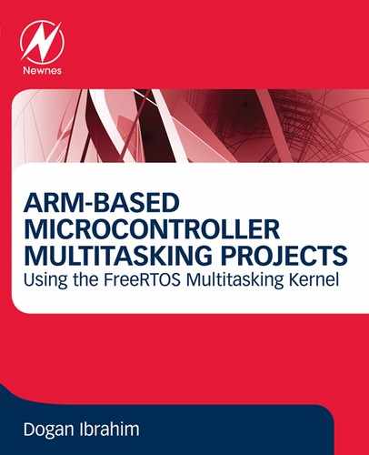
The Interrupt Assistant utility of mikroC can be used to create ISR templates. To use the Interrupt Assistant, start the mikroC IDE and click on Tools -> Interrupt Assistant. You should see a form as in Fig. 6.2. Enter the desired ISR function name (e.g., button), choose the type of interrupt source (e.g., INT_TIM2), choose the ICS parameter (e.g., AUTO) and then click OK (see Fig. 6.3). The following ISR code template will be automatically generated:
void button() iv IVT_INT_TIM2 ics ICS_AUTO {
}
Figure 6.2Interrupt Assistant form.
Figure 6.3Interrupt Assistant example.
6.9. Creating a new project
The aim of the project created in this section is to show how to develop a project, then how to compile and upload the executable code to the program memory of the target processor. In this section, we will flash the LED connected to port pin PE12 of the Clicker 2 for STM32 development board every second. In this project we shall be using the external 25 MHz crystal as the timing source.
The steps in creating a new mikroC project are given below:
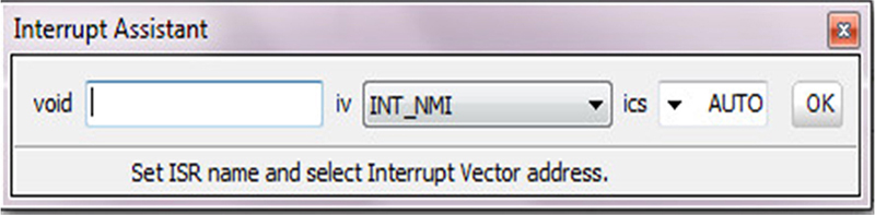
•Step 1: Start the mikroC Pro for ARM IDE by clicking on its icon. Fig. 6.4 shows parts of the IDE screen.
•Step 2: Create a new project by clicking New Project. Select Standard project and click Next. As shown in Fig. 6.5, give a name to your project (e.g., LED) and specify a folder (e.g., D:ARM). Choose the device name as STM32F407VG and set the device clock to 168MHz. Click Next. Click Finish and you should see the main IDE window shown in Fig. 6.6.
Figure 6.4mikroC IDE screen.
Figure 6.5Create a new project.
Figure 6.6Main IDE window.
The parts of the screen are as follows:
1. Top Menu Bar. There are icons just at the bottom of the Menu Bar for quick access to various features and tools of the IDE.
2. The Code Explorer is located at the top left corner of the screen. You can see a list of functions, weblinks, and active comments in the project you opened.
3. Project Settings. In this section, you have the name of the device you are using, and the frequency of the microcontroller clock. The frequency of the clock determines the speed of the microcontroller.
4. Select the build or debugger type. You should select Release for the Build Type.
5. Messages. In case that errors were encountered during compiling, the compiler will report them in the Message box, and a hex file will not be generated. The compiler also reports warnings, but these do not affect the output; only errors can interfere with the generation of a successful hex file.
6. The Code Editor features adjustable Syntax Highlighting, Code Folding, Code Assistant, Parameters Assistant, Auto Correct for common typos, and Code Templates.
7. The Project Manager is an IDE feature which allows you to manage multiple projects. It shows source and header files in each project. Several projects can be open at the same time, but only one of them may be active at any one time. To set a project in an active mode you need to double click on the desired project in the Project Manager.
8. The Library Manager allows you to work with the libraries in a simple and easy way. The Library Manager window lists all libraries. The desired library is added to the project by selecting the checkbox next to the library name. In order to have all library functions available, simply press the Check All button, and that’s it.
9. Project Explorer.
10. Libstock Manager. See a list of the recent Click boards and install the software and the SDK (Software Development Kit) if required.
Step 3: You should now see a code template with just main. Type in the program code given in Fig. 6.1. The screen should look as in Fig. 6.7.
Figure 6.7Write your program.
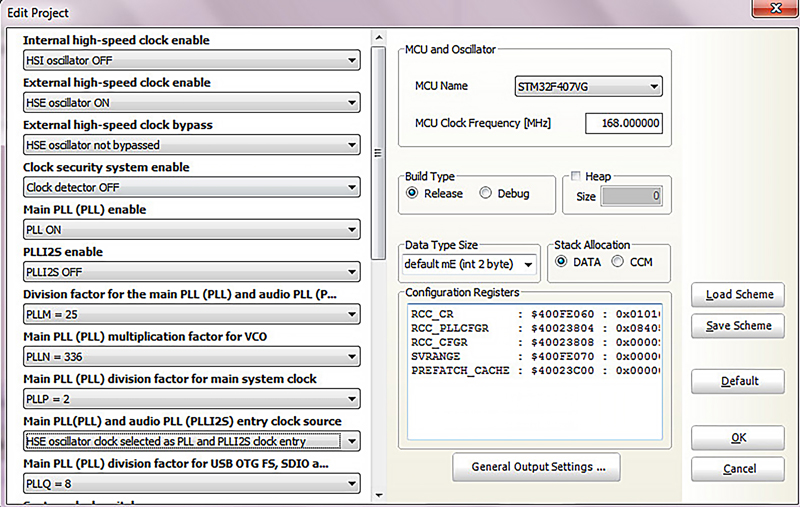
Step 4: We should now set the clock for our project. This is one of the important steps when a new project is created. Click Project -> Edit Project. Set the clock to use external high-speed clock. Fig. 6.8A and B shows the required settings to operate at 168 MHz (see Chapter 2 for details of clock settings).
The various clock configuration options are explained below in reference to Fig. 6.8A and B.
Internal high-speed clock enable: This option is used to enable/disable the internal 16 MHz high-speed clock HSI.
External high-speed clock enable: This option is used to enable/disable the external high-speed clock HSE.
External high-speed clock bypass: If the External high-speed clock HSE is enabled and at the same time External high-speed clock is bypassed, then it is assumed that an external clock generator circuit (i.e., not a crystal) is connected to the OSC_IN pin of the microcontroller.
Clock security system enable: This option is used to enable/disable the clock security system. When enabled, if there is an error in the HSE oscillator, the HIS oscillator automatically starts running and generates a clock for the microcontroller. At the same time, an interrupt is generated.
Main PLL enable: This option enables/disables the PLL block.
PLLI2S enable: This option enables/disables the PLLI2S block.
Division factor for the man PLL and Audio PLL (PLLI2S) input clock: This option selects the main PLL division factor. This is shown as PLL_M in Fig. 6.8.
Main PLL (PLL) multiplication factor for VCO: This option is used to select the main PLL multiplication factor for VCO. This is shown as PLL_N in Fig. 6.8.
Main PLL (PLL) division factor for main system clock: This option is used to select the AHB prescaler. It is shown as PLL_P in Fig. 6.8.
Main PLL (PLL) and audio PLL (PLLI2S) entry clock source: This option is used to select the PLL block that provides clock to the Main PLL and to the I2S. The HSE or HIS clocks can be selected from here. This is shown as PLL Source Clock in Fig. 6.8.
Main PLL (PLL) division factor for USB OTG FS, SDIO and random number generator clocks: Select the division factor for USB, SDIO and random number generator. This is shown as PLL_Q in Fig. 6.8.
System clock switch: This is used to select the system clock either from HIS, HSE, or PLL.
Set and cleared by software to control the division factor of the AHB clock: This is used to select the division factor to derive the AHB clock from the system clock SYSCLK. This is shown as AHBx Prescaler in Fig. 6.8.
APB low-speed prescaler (APB1): This is used to select the low-speed APB1 clock (PCLK1). It is shown as APB1 Prescaler in Fig. 6.8.
APB high-speed prescaler (APB2): This is used to select the high-speed APB2 clock (PCLK2). It is shown as APB2 Prescaler in Fig. 6.8.
HSE division factor for RTC clock: This option is used to select the division factor for the RTC clock.
Microcontroller clock output 1: This option is used to select the microcontroller clock output (MCO1) from either HIS, HSE, LSE, or PLL.
I2S clock selection: This option is used to select the I2S clock source. The PLLI2S or external clock source connected to the I2S_CKIN pin can be selected.
MCO1 prescaler: This option is used to select the MCO1 output clock prescaler.
MCO2PRE: This option is used to select the MCO2 prescaler.
Microcontroller clock output 2: This option is used to select the microcontroller clock 2 output (MCO2) either from SYSCLK, PLLI2S, HSE, or PLL.
Voltage range: Use this option to select voltage range.
Prefetch and cache option: This option is used to enable or disable the prefetch and cache if we wish to store data in the flash memory area.
It is important that the following rules are obeyed while configuring the clock:
• The frequency to the input of the PLL modules must be between 1 and 2 MHz.
• The frequency at the output of the PLL modules must be between 64 and 432 MHz.
• The USB frequency must be 48 MHz.
• Make sure that PLL_N > 1, PLL_Q > 1, and PLL_P = 2, 4, 6, or 8.
• AHB frequency must not be greater than 168 MHz.
• APB1 frequency must not be greater than 42 MHz.
• APB2 frequency must not be greater than 84 MHz.
An example is given below to illustrate how the clock configuration can be done in a new project.
Example
It is required to configure the clock to use the internal high-speed clock (16 MHz) and operate the STM32F407VGT6 microcontroller with 168 MHz. Assume that the RTC, USB, or I2S are not used in this application.
Solution
The required clock settings are:
Internal high-speed clock:
ON
External high-speed clock:
OFF
External high-speed clock bypass:
HSE oscillator not bypassed
Clock security system enable:
Clock detector OFF
Main PLL (PLL) enable:
PLL ON
PLLI2S enable:
PLLI2S OFF
Division factor for the main PLL and…:
PLLM = 16
Main PLL (PLL) multiplication factor:
PLLN = 336
Main PLL (PLL) division factor for main..:
PLLP = 2
Main PLL (PLL) and Audio PLL (PLLI2S):
HSI oscillator clock selected as PLL…
Main PLL (PLL) division factor for USB..:
(not important here)
System clock switch:
PLL selected as system clock
Set and cleared by software to control the…:
SYSCLK not divided
APB low-speed prescaler (APB1):
HCLK divided by 4
APB high-speed prescaler (APB2):
HCLK divided by 2
HSE division factor for RTC clock:
no clock
Microcontroller clock output 1:
(not important here)
I2S clock selection:
(not important here)
MCO1 prescaler:
(not important here)
MCO2PRE:
(not important here)
Microcontroller clock output 2:
(not important here)
Voltage range:
2.7–3.6 V
Prefetch and cache option:
(not important here)
In this example the internal 16 MHZ HSI clock is divided by 16 to give 1 MHZ and is then multiplied by 336 to give the 336 MHz and divided by 2 to give the 168 MHz system clock.
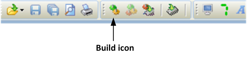
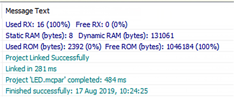
Step 5: We are now ready to compile the program. Click Build->Build or click the Build icon (see Fig. 6.9). Your program should compile with no errors as shown in Fig. 6.10. Notice that memory usage and compilation time are given at the bottom of the screen inside the message window. The compiler generates various files, such as the assembly listing, HEX file, configuration file and so on (some of these files are generated optionally). The important file is the HEX file as it is used to upload the program memory of the target microcontroller.
Figure 6.9Build icon.
Figure 6.10Program compiled with no errors.
6.9.1. Uploading the executable code
The microcontroller on the Clicker 2 for STM32 development board can be programmed using the Bootloader firmware which has already been loaded to the microcontroller memory by the manufacturers. We need to install the mikroBootloader software to our PC so that we can upload our executable code to the program memory of the target processor. The steps to install the mikroBootloader are as follows:
• Click on clicker 2 STM32 Bootloader at the bottom of the screen
• Copy the software to a folder of your choice (e.g., to Desktop)
The steps to upload the executable code to the microcontroller memory are as follows:
• Connect the Clicker 2 for STM32 development board to your PC using a mini USB cable, and turn on the power switch. You should see the green power LED to turn ON.
• Start the mikroBootloader on your PC.
• Press and release the red Reset button next to the power switch on your development board.
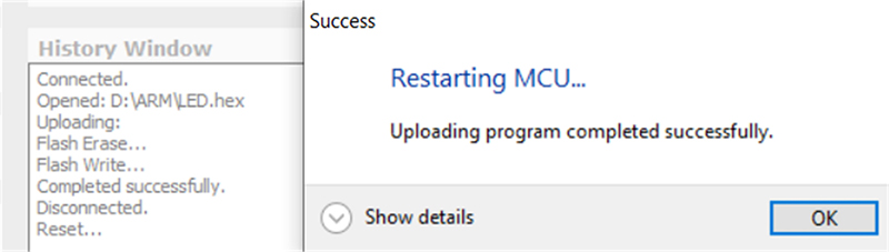
• Click the Connect button on the mikroBootloader application as soon as possible (you should do this within 5 s, otherwise the microcontroller performs a hardware reset and starts executing the previously loaded user program—if there is already one). You should see the Connected message (see Fig. 6.11).
• Click the Browse for HEX button and select the HEX file of your application program (Fig. _6.12). You should see a message similar to:
• Opened: D:ARMLED.hex
• Click Begin uploading to start uploading the executable code to the program memory of the microcontroller on your development board. You should see a successful upload message as shown in Fig. 6.13.
• If everything went well then you should see the red LED on the development board flashing every second.
Figure 6.11Connect the mikcroBootloader to the development board.
Figure 6.12Select the HEX file of your application.
Figure 6.13Uploading the executable code to target processor.
6.10. Simulation
Simulation is a useful tool during program development as it helps to detect programming errors at an early stage before the code is loaded to the program memory of the target microcontroller. Simulation is normally carried out on a PC and it can be used to single-step through a program, to set breakpoints, and to view and modify processor registers and variables used in the program. In this section we will be seeing how to simulate the simple LED flashing program developed in the previous section.
The steps to simulate our program are given below:
Step 1: Click Run -> Start Debugger. The simulation window will open on the right-hand side as shown in Fig. 6.14. The blue bar across the screen shows where the program step is currently located and it should be at the beginning of the program by default.
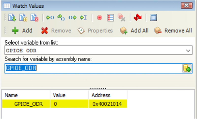
Step 2: Let us view the contents of PORTE as the program is run in single-step mode. Select PORTE output register GPIOE_ODR and click Add (the + sign). PORTE will be added to the window (see Fig. 6.15) so that we can view its values as the program is run. Its value is shown as 0 at the moment.
Step 3: Keep pressing F8 to single-step through the program. You should see the blue bar moving through the program as the key is pressed.
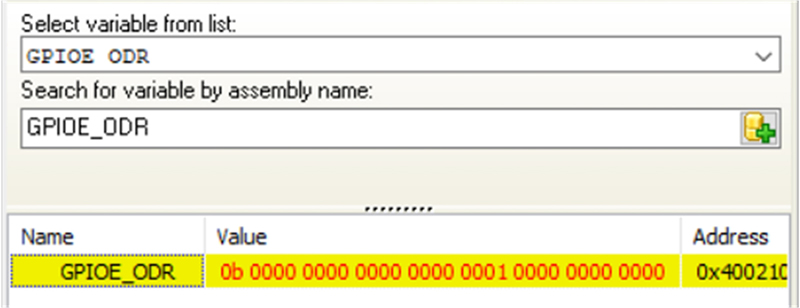
Step 4: You should see the data at PORTE changing when the port value is toggled. Click on the value in the simulation window to change the output data from decimal to binary (see Fig. 6.16). You should see the port value displayed as 0000 0000 0000 0000 0001 0000 0000 0000, as shown in Fig. 6.17 where PE12 is set to 1.
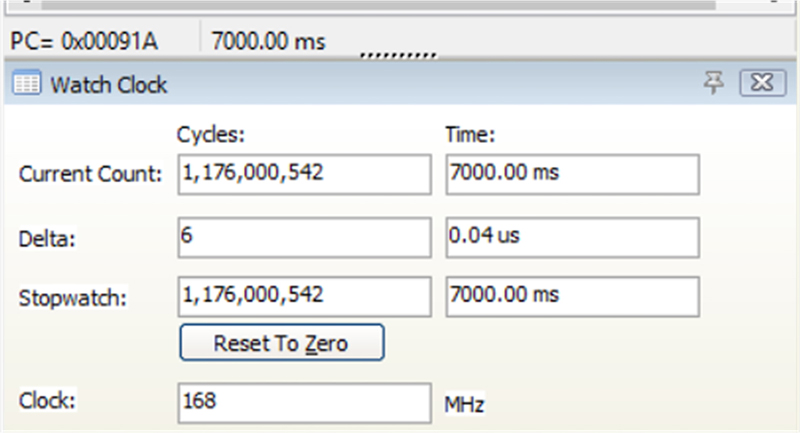
Step 5: As you single-step through the program, port PE12 value will change between 0 and 1. Simulation timing statistics are shown at the bottom of the simulation window (see Fig. 6.18)
Figure 6.14Simulation window.
Figure 6.15Add GPIOE_ODR to the simulation window.
Figure 6.16Change output value to hexadecimal.
Figure 6.17Port value changing to 0xFFFF.
Figure 6.18Simulation timing statistics.
6.10.1. Setting break points
Breakpoints are useful especially while testing large and complex programs. By setting a breakpoint in a program, we allow the program to run up to the breakpoint and then we can examine or modify the values of various registers and variables. An example is given in this section to show how a breakpoint can be set and variables examined in our program.
Step 1: Start the simulator as described in the previous section.
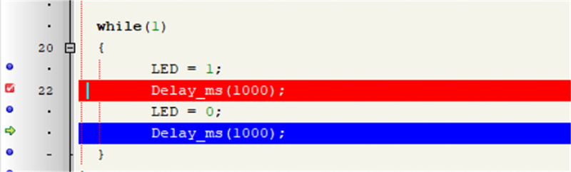
Step 2: Let us set a breakpoint at the instruction Delay_ms(1000). Put the cursor on this instruction and then click Run -> Toggle Breakpoint (or click F5). You should see a red bar at the breakpoint (see Fig. 6.19) and also a small arrow on the left-hand side of the instruction where the breakpoint is placed.
Step 3: Now run the program by clicking Run -> Run/Pause Debugger (or click F6). The program will run-up to the breakpoint and then stop. You can now view the output data of PORTE as shown earlier.
Step 4: You can remove the breakpoint by clicking Run -> Toggle Breakpoint or by clicking on the small arrow on the left-hand side of the instruction where the breakpoint is placed.
Figure 6.19Setting a breakpoint.
6.11. Debugging
Debugging is similar to simulation but is carried out on the target hardware. The hardware to be debugged usually consists of the complete project hardware including all the peripheral devices. By debugging we try to find errors in a program or in associated hardware (although only a limited number of hardware errors can be detected by the process of debugging).
In a typical debugging session, the developed program is uploaded to the program memory of the target microcontroller and then the actual debugging takes place while the program runs in real-time on the target microcontroller. As in simulation, the code can be single-stepped and breakpoints can be inserted into the code and registers and variables can easily be examined or modified as desired.
Unfortunately, we cannot run the debugger with the Clicker 2 for STM32 development board as it requires a hardware programmer device to be connected to the development board. But the steps for debugging are similar to the steps for simulation. The Build/Debugger type panel should be set to Debug and Hardware before the debugger can be started.
6.12. Other mikroC IDE tools
mikroC IDE includes many other useful tools that can be used during program development. Some commonly used tools are described in this section.
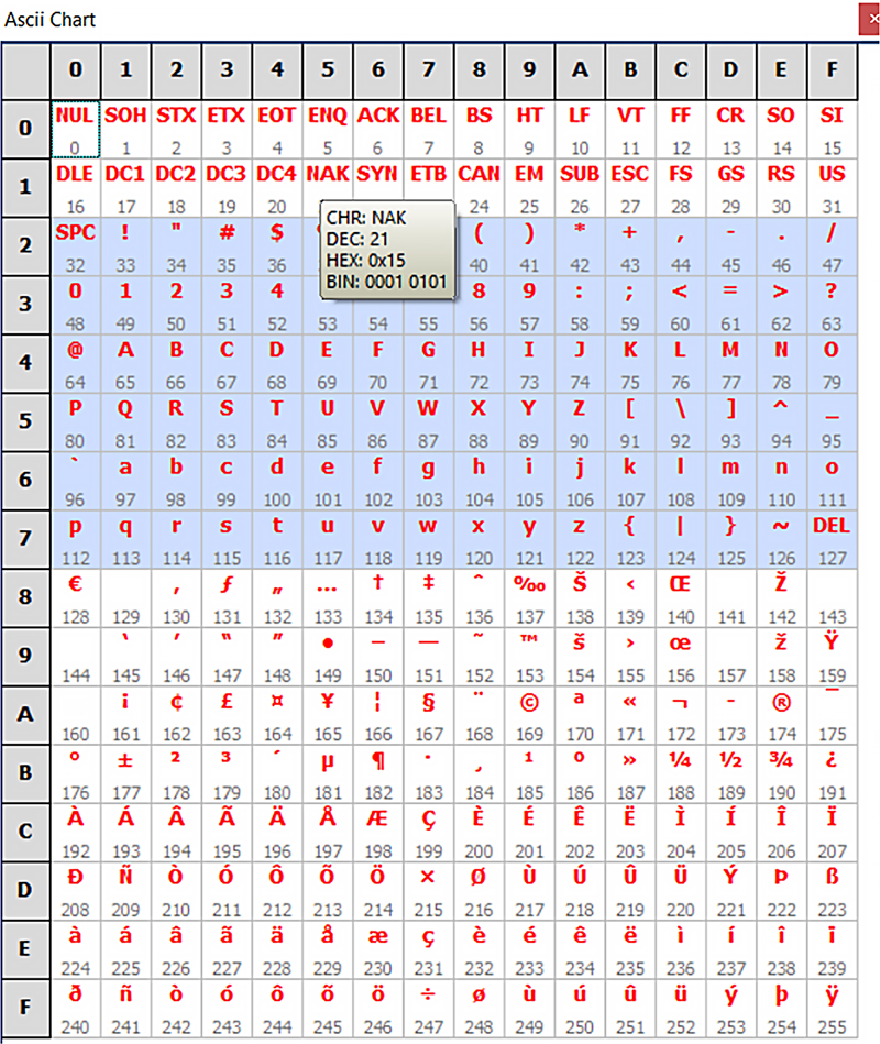
6.12.1. ASCII chart
This tools is accessed from Tools -> Ascii Chart and it displays the standard ASCII chart as shown in Fig. 6.20.
Figure 6.20ASCII chart tool.
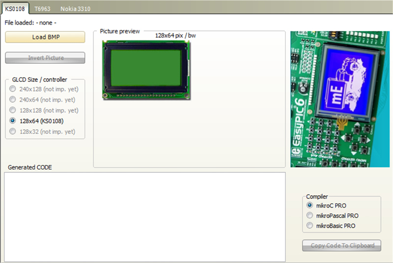
6.12.2. GLCD bitmap editor
This tool is accessed from Tools -> GLCD Bitmap Editor and it helps to design a bitmap for the GLCD displays. Fig. 6.21 shows the editor tool.
Figure 6.21GLCD bitmap editor.
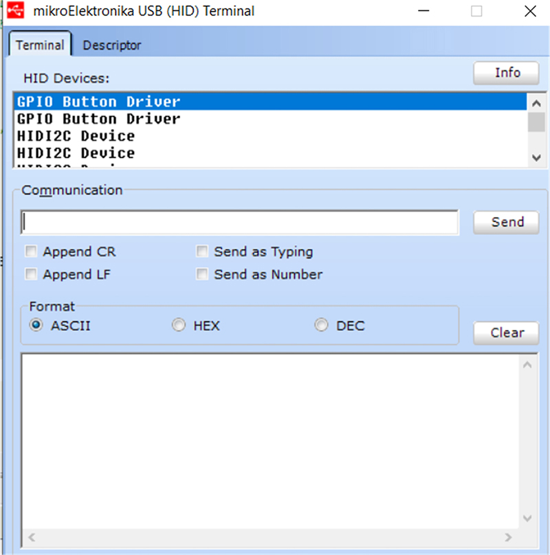
6.12.3. HID terminal
This tool is accessed from Tools -> HID terminal and it is useful while developing USB based applications. Fig. 6.22 shows this tool.
Figure 6.22HID terminal tool.
6.12.4. Interrupt assistant
This tool helps to create an ISR template as described in an earlier section.
6.12.5. LCD custom character
This tool is accessed from Tools -> LCD Custom Character and it can be used to create code for custom characters for standard LCD displays. Fig. 6.23 shows this tool.
Figure 6.23LCD custom character tool.
6.12.6. Seven segment editor
This tool is accessed from Tools -> Seven Segment Editor and it can be used to create a pattern for standard seven-segment displays. Fig. 6.24 shows this tool.
Figure 6.24Seven segment editor tool.
6.12.7. UDP terminal
This tool is accessed from Tools -> UDP Terminal and it is useful while developing UDP based communications programs. Fig. 6.25 shows this tool.
Figure 6.25UDP terminal tool.
6.12.8. USART terminal
This tool is accessed from Tools -> USART Terminal and it is useful while developing RS232 based serial communications programs. Fig. 6.26 shows this tool.
Figure 6.26USART terminal tool.
6.12.9. USB HID bootloader
This tool is accessed from Tools -> USB HID Bootloader and it can be used to upload code to microcontrollers that have already been loaded with bootloader programs. Fig. 6.27 shows this tool.
Figure 6.27USB HID bootloader tool.
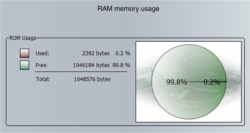
6.12.10. Statistics
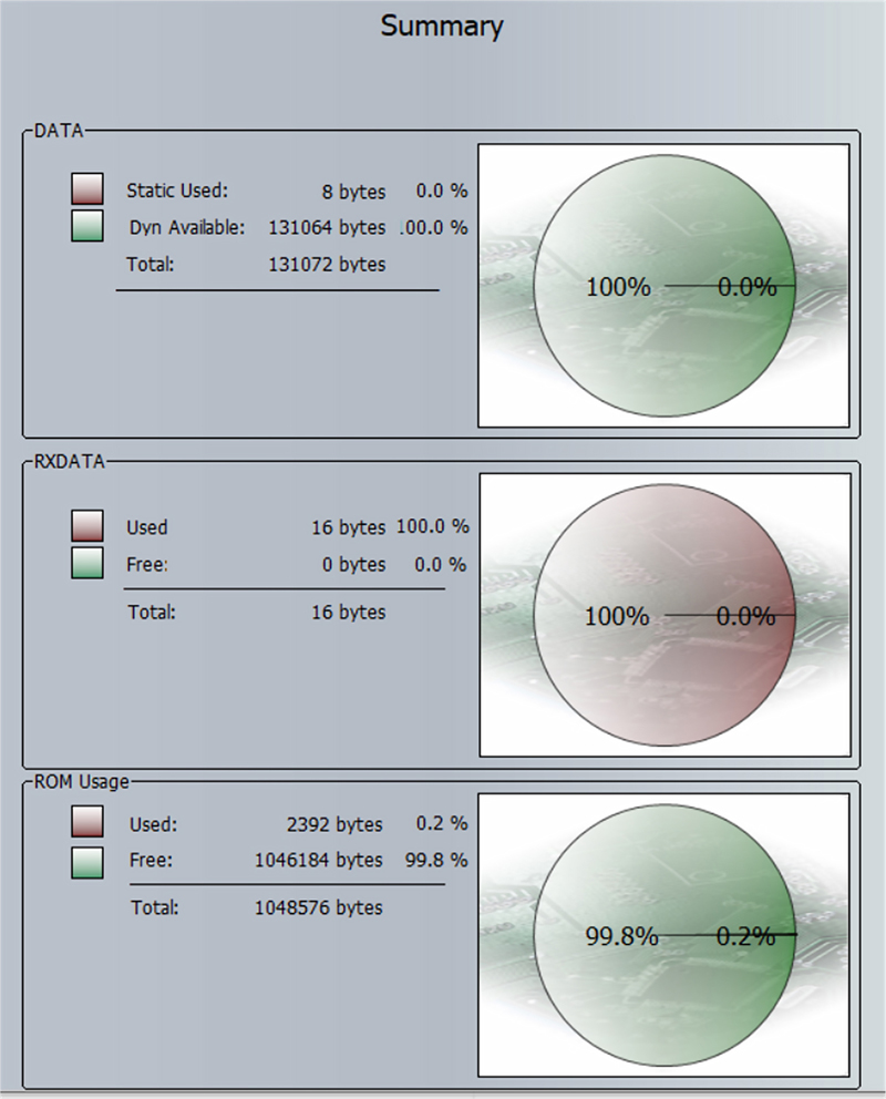
Program statistics can be seen by using the tool View -> Statistics. For example, Fig. 6.28 shows the RAM usage statistics. Similarly, Fig. 6.29 shows the ROM memory usage statistics. A summary screen is also available as shown in Fig. 6.30.
Figure 6.28RAM usage statistics.
Figure 6.29ROM usage statistics.
Figure 6.30Summary screen.
6.12.11. The library manager
A list of the library functions included in a project can be seen using the menu option View -> Library Manager. Additional libraries can be added to a project if desired by clicking at the left hand side of the desired library name in the Library Manager. Fig. 6.31 shows part of the library manager screen.
Figure 6.31The library manager.
6.12.12. Assembly listing
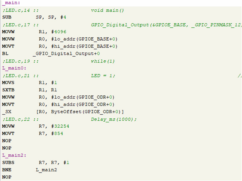
The assembly listing of the program can be displayed by clicking View->Assembly as shown in Fig. 6.32.
Figure 6.32Assembly listing.
6.12.13. Output files
A list of the output files generated by the compiler can be seen by clicking Output Files in the Project Manager window as shown in Fig. 6.33. The most important output file is the HEX file since this is the file which is uploaded to the microcontroller program memory.
Figure 6.33Output files.
6.12.14. Options window
Clicking the Options icon displays various IDE options that can be set by the user. An example is shown in Fig. 6.34.
Figure 6.34Options window.
6.13. Summary
This chapter has described the features of the mikroC Pro for ARM programming language and IDE. The ARM Cortex-M4 specific features of this language have been given briefly with examples where appropriate. The chapter has also shown how to create a new project using the IDE, and then how to compile and upload the generated HEX code to the Clicker 2 for STM32 development board program memory. Additionally, the steps in simulating a program in software have been described in detail. Finally, some of the useful tools of the mikroC IDE are shown with their screen views.
Next Chapter makes an introduction to multitasking which is the main topic of this book. The chapter describes the basic principles of some of the commonly used multitasking scheduling algorithms.