There are over a thousand different types of microcontrollers, manufactured by many companies. The choice of the best microcontroller for a particular application has become rather difficult as the user is faced with many options. Briefly, this choice depends on many factors, such as the cost, speed, power consumption, size, data width, support of peripheral devices, reliability, availability of compilers, simulators, debuggers, etc. This chapter is about the ARM family of microcontrollers and it describes the basic features of the Cortex-M, Cortex-R, and Cortex-A processors. The compatibility of the various Cortex-M processors is described briefly in this chapter. The chapter also describes the architecture and basic features of the STM32F407 family of ARM-based microcontrollers. This is the microcontroller used in all the projects in this book. Various components of the STM32F407 microcontroller are described, such as the memory organization, clock circuitry, timers, and input-output circuits.
Keywords
ARM microcontroller
Cortex-M
Cortex-R
Cortex-A
Cortex-M compatibility
ARM performance
STM32F407 family
STM32F407 architecture
nested vectored interrupts
2.1. Overview
It is important to learn the basic architecture, advantages, disadvantages, and limitations of a microcontroller before it is used in a project. This concept is more important if one is going to use assembler programming. It is still important to know the basic internal block diagram and the input-output structure if one is going to program using a high-level language. In this book we shall be using the highly popular 32-bit ARM microcontroller, the STM32F407VGT6 in all the projects, together with the mikroC Pro for ARM high-level language. This microcontroller is a member of the STM32 family of ARM microcontrollers. A brief description of the architecture of this microcontroller is given in this chapter and its basic features are described so that we can develop projects easily and efficiently.
Clock configuration and input-output ports are important parts of every microcontroller and are used almost in all projects. As a result, these are described in detail in this chapter.
2.2. ARM microcontrollers
There are over a thousand different types of microcontrollers manufactured by many companies. The choice of the best microcontroller for a particular application has become rather difficult as the user is faced with many options. Briefly, this choice depends on many factors, such as:
• Cost
• Speed
• Power consumption
• Working voltage
• Size
• Data width (8, 16, 32 bit?)
• Program and data memory capacity
• Number of general purpose digital input-output ports
• Number of analog input ports (ADC) and their precisions
• Number of digital-to-analog converter (DAC) ports and their precisions
• Interrupt support
• Number of timers and their precisions
• UART support
• Special bus support (I2C, SPI, CAN USB, etc.)
• Availability of development boards
• Availability of compilers, simulators, debuggers, and programmers (e.g., integrated development environment)
• Hardware and software support available
• Compatibility with commonly available external devices and components (e.g., sensors, actuators, Wi-Fi modules, Bluetooth modules, etc.)
• Availability of the chosen microcontroller
• Reliability of the chosen microcontroller (e.g., temperature range, operation under vibration and shock, failure rate, etc.)
For example, if the microcontroller is to be used in a battery-operated children’s toy then the two most important requirements are the low cost and low power consumption. High performance is not normally a requirement in such applications unless the toy is a fast graphical game. If on the other hand the microcontroller is to be used in a flight controller equipment, then the performance, reliability, and data width are some of the most important factors to consider while making a choice. Similarly, reliability, safety, and power consumption are important factors in most portable medical applications. In games-based applications with graphical displays and keyboards, very high speed and low power consumption are the two most important factors. If the application is to control the temperature of a chemical plant then the important factors could be the reliability, precision of the ADC and the DAC, timer support, and interrupt support. In most hobby type application, one can in general choose a general purpose microcontroller that satisfies the following criteria: low cost, adequate speed, enough number of input-output ports, required numbers of ADC and DAC, and support for special bus support modules such as SPI and/or I2C. The size, memory capacity, timer support, interrupt support, data width, and working voltage are not important factors since almost all microcontrollers provide enough support for these items. In general, as the clock speed goes up so does the power consumption and the cost, and as a result a trade-off should be made in choosing a microcontroller for a specific application.
ARM has been designing high performance and low-cost 32-bit microcontrollers for over 20 years and in the last few years they have also started to offer 64-bit designs in addition to their 32-bit systems It is important to know that ARM does not manufacture or sell any processors or chips. In fact, they design the core processor architecture and make money by licensing their designs to various chip manufacturers. The manufacturers use the core ARM processors (the core CPU) and integrate them with their own peripherals to create complete microcontrollers. For example, manufacturers add their memory modules, input-output, interrupt modules, timer modules, ADC and DAC, etc. to the core CPU processors to make a complete working microcontroller. ARM’s core architecture does not include graphics controllers, wireless connectivity, or any other form of peripheral modules. ARM is then given royalty fees for each chip manufactured by the third party companies. Companies that use ARM core CPU processors include, Atmel, Broadcom, Apple, Freescale Semiconductors, Analog Devices, Texas Instruments, NXP, Samsung Electronics, Nvidia, Qualcomm, Renesas, STMicroelectronics, and many others.
ARM was originally known as the Acorn Computers and they have developed the first Acorn RISC Machine (ARM) architecture in the 1980s to use in their personal computers. The first ARM processors were coprocessor modules used in the old and famous BBC Micro series. After failing to find suitable high-performance microprocessor chips in the market, Acorn decided to design and use their own processors. In 1990, the research section of Acorn formed ARM Ltd. Today, known as the ARM Holdings Ltd, their headquarters are based in Cambridge (UK) and is owned by the Japanese telecommunications company SoftBank Group. As in the year 2010, ARM market share was over 95% in the smartphone market, 10% in mobile computers, 35% in smart TVs. In the year 2014, over 50 billion chips with the ARM core processors were manufactured in the world.
The main feature of the ARM core processors is their low power consumption, which makes them ideal processors in battery-operated portable applications. Nowadays, almost all mobile phones contain ARM core processors as their main CPUs. Recently, the highly popular Raspberry Pi single-board computer uses ARM processors in all of their CPUs. The low power consumption, small size, and low cost make ARM an ideal processor in embedded applications. ARM processors are based on an instruction set called Thumb. This instruction set cleverly takes 32-bit instructions and compresses them down to 16-bits, thus reducing the hardware size and consequently the overall cost. Although Thumb is easy to learn and use, almost all applications make use of a high-level language, such as C, C++, Python, etc. Complex multistage pipelined architecture is used inside the processors in order to increase the throughput significantly.
ARM processors have the RISC (reduced instruction set computer) architecture where only a small number of instructions is used in their instruction sets. Compared to CISC (complex instruction set computer) architectures, RISC results in higher speed since the unimportant and not frequently used instructions are removed and the data ways are optimized to result in superior performance.
ARM has developed many 32-bit processors over the last several decades. Around the year 2003, ARM decided to improve their market share by developing a new family of high-performance processors. These processors were aimed for general purpose microcontroller-based industrial, domestic, and the consumer market applications. As a result, the highly popular Cortex family of processors was created. Depending on the throughput and complexity of the core processor, this family consists of three processor families: Cortex-M, Cortex-R, and Cortex-A. Brief details of these family of processors are given below.
2.2.1. Cortex-M
Cortex-M series has been targeted specifically for the crowded MCU market where there are already many types of microcontrollers. This family was first released in 2004 and soon gained popularity. Cortex-M has become the most popular 32-bit microcontroller in the market since its introduction and one can easily say that it has become the industry standard microcontroller. There are basically five processor families within the Cortex-M family: Cortex-M7, Cortex-M4, Cortex-M3, and Cortex-M0, and Cortex-M0+. Brief details of these families are given below.
2.2.1.1. Cortex-M7
This is the highest performance Cortex-M processor. With the built-in floating point unit, the power consumption is reduced and thus the battery life is extended. The processor is based on 6-stage pipeline with branch prediction. The performance is 3.23 DMIPS/MHz, consuming 33 μW/MHz.
2.2.1.2. Cortex-M4
Cortex-M4 is built using the ARMv7-M architecture. These are high-performance microcontrollers having DSP and floating point arithmetic capabilities with high throughputs. The performance is 1.95 DMIPS/MHZ with a 3-stage pipeline, and clock speeds up to 200 MHz. The processor consumes 32.82 μW/MHz. This family uses the Thumb-2 instruction set with special instructions for handling DSP algorithms and floating point operations. If the application requires floating point maths then Cortex-M4 is probably one of the best choices. The STM32F407 microcontroller used in this book is based on the Cortex-M4 architecture.
2.2.1.3. Cortex-M3
Cortex-M3 is also based on the ARMv7-M architecture and its architecture is very similar to Cortex-M4. The performance and clock speed of Cortex-M3 is slightly lower than the Cortex-M4. The performance of Cortex-M3 is 1.89 DMIPS/MHz and it consumes 31 μW/MHz. The significant difference between Cortex-M4 and Cortex-M3 is that Cortex-M3 does not include a DSP processor or a floating point module. If the application does not need to use the DSP functionality, then it may be more appropriate to choose a member of the Cortex-M3 family.
2.2.1.4. Cortex-M0+
The smallest members of the Cortex-M family are Cortex-M0+ and Cortex-M0. The performance of Cortex-M0+ is 1.35 DMIPS/MHZ, but it is still compatible with other Cortex-M family members. The processor consumes only 9.85 μW/MHz. Cortex-M0+ uses a subset of the Thumb-2 instruction set (Thumb) and is based on a 2-stage pipeline architecture. Although the performance is lower, there is overall power saving compared to its bigger brothers. Cortex-M0+ also features advanced debug options.
2.2.1.5. Cortex-M0
This is the smallest processor in the Cortex-M family, having a gate count of only 12K, consuming 12.5 μW/MHz. The processor reduces memory requirements where the on-chip flash memory is optimized to save cost, reduce power, and increase performance. The processor uses 3-stage pipeline with a subset of the Thumb-2 instruction set (Thumb). The performance is 1.27 DMIPS/MHZ. The low cost of the processor enables the developers to achieve 32-bit performance at an 8-bit price.
2.2.2. Cortex-R
Cortex-R family are real-time higher performance processors than the Cortex-M family. Some members of this family are designed to operate at clock speeds in excess of 1 GHz. The main application areas of these processors are hard-disk controllers, automotive applications, network devices, and specialized high-speed applications. Early members of this family, Cortex-R4 and Cortex-R5, operate at clock speeds of up to 600 MHz. Cortex-R7 incorporates 11-stage pipeline and it can operate with clock speeds in excess of 1 GHz. Although the Cortex-R processors are high performance, their architectures are complex and they consume high power, making them unsuitable for use in mobile battery-powered devices. The performance of Cortex-R7 is 3.77 DMIPS/MHz. Cortex-R52 is a faster member of the family, having a performance of 5.07 DMIPS/MHz.
2.2.3. Cortex-A
Cortex-A family is the highest performance ARM processor family used in real-time operating systems, mainly in mobile applications, such as in mobile phones, tablets, GPS devices, electronic games, and so on. These processors support advanced features required for the design of mobile operating systems, such as ioS, Android, Linux, etc. Additionally, advanced memory management is supported by these processors with virtual memory. Early members of the family include processors such as Cortex-A5 to Cortex-A17, based on the ARMv7-A architecture. Latest members of the family are the Cortex-A50 and Cortex-A72 series designed for lower power and very high-performance mobile applications. These processors are built using the ARMv8-A architecture which offers 64-bit energy efficient operation with the capability of more than 4 GB of physical memory.
2.2.4. Cortex-M processor comparison
Table 2.1 shows a comparison of various Cortex-M family of processors. As can be seen from this table, Cortex-M0 and Cortex-M0+ are used at low speed and low power consumption applications. Cortex-M1 is optimized for use in programmable gate array applications. Cortex-M3 and Cortex-M4 are medium power processors used in microcontroller applications with the Cortex-M4 supporting DSP and floating point arithmetic operations. Cortex-M7 is a high-performance member of the family which is used in applications requiring higher performance than the Cortex-M4.
Table 2.1
Cortex-M processor comparison.
Cortex processor
Description
Cortex-M0
Low power consumption, low to medium performance, smallest ARM processor
Cortex-M0+
Lower power consumption and higher performance than Cortex-M0
Cortex-M1
Designed mainly for gate array applications
Cortex-M3
Very popular, low power consumption, medium performance, debug features, used in microcontroller type applications
Cortex-M4
Similar architecture to Cortex-M3 but includes DSP and floating point arithmetic, used in high end microcontroller type applications
Cortex-M7
High performance processor, used in applications where Cortex-M4 is not fast enough, supports DSP and single and double precision arithmetic
2.2.5. Cortex-M compatibility
Processors in the Cortex family are upward compatible with each other. Cortex-M0 and Cortex-M0+ are based on the ARMv6-M architecture, using the Thumb instruction set. Cortex-M4 and Cortex-M7 are based on the ARMv7-M architecture, using the Thumb-2 instruction set which is a superset of Thumb. Although the architectures are different, software developed on the Cortex-M0 and Cortex-M0+ processors can run on Cortex-M3, Cortex-M4, and Cortex-M7 processors without any modifications provided the required memory and input-output ports are available.
2.2.6. Processor performance measurement
Processor performance is usually measured using benchmark programs. There are many benchmark programs available and one should exercise care when comparing the performance of various processors as the performance depends on many external factors, such as the efficiency of the compiler used, and the type of operation performed for the measurement.
Many attempts were made in the past to measure the performance of a processor and quote it as a single number. For example, MOPS, MFLOPS, Dhrystone, DMIPS, BogoMIPS, and so on. Nowadays, CoreMark is one of the most commonly used benchmark programs used to indicate the processor performance. CoreMark is developed by Embedded Microprocessor Benchmark Consortium (EEMBC, www.eembc.org/coremark) and is currently one of the most reliable performance measurement tools available.
Table 2.2 shows the CoreMark results for some of the commonly used microcontrollers. As can be seen from this table, Cortex-M7 achieves 5.01 CoreMark/MHz, while the medium range PIC18 microcontroller achieves only 0.04 CoreMark/MHz.
Table 2.2
CoreMark/MHz for some commonly used microcontrollers.
Processor
CoreMark/MHz
Cortex-M7
5.01
Cortex-A9
4.15
Cortex-M4
3.40
Cortex-M3
3.32
Cortex-M0+
2.49
Cortex-M0
2.33
dsPIC33
1.89
MSP430
1.11
PIC24
1.88
PIC18
0.04
2.3. The STM32F407VGT6 microcontroller
The STM32 family of 32-bit microcontrollers is based on ARM Cortex and there are over 300 compatible devices in the family. As described below, the family includes microcontrollers with the Cortex-M4, Cortex-M3, and Cortex-M0 architectures.
In this book we shall be using the highly popular ARM-based microcontroller STM32F407VGT6 together with the Clicker 2 for STM32 development board (details are given in a later chapter). In the remaining sections of this chapter, we shall be looking at the features of the STM32F407VGT6 microcontroller. The internal architecture of this microcontroller is very complex and we shall only look at the important modules used in most projects, such as I/O, timers, ADC and DAC converters, interrupts, I2C, USART, and so on. Interested readers can get detailed information from manufacturers’ data sheets and application notes available for download on the Internet.
2.3.1. Basic features of the STM32F407VGT6
The STM32F407VGT6 microcontroller is based on the Cortex-M4 architecture and has the following basic features:
• ARM Cortex-M4 32-bit RISC architecture
• Included floating point unit (FPU) and digital signal processor (DSP)
• Up to 168 MHz maximum operating frequency
• Single-cycle multiplication and hardware division
• Up to 1 Mb of flash memory
• Up to 192 Kb of SRAM
• 1.8–3.6 V power supply
• −40°C to +105°C operation
• Clock PLL
• 4–26 MHz external crystal
• Internal 16 MHz RC clock
• Internal 32 kHz oscillator for RTC
• Low power with sleep, stop, and standby modes
• 3 × 12-bit 24 channel ADC converters with 0–3.6 V reference voltage
• Sample and hold capability
• Temperature sensor
• 2 × 12-bit DAC converters
• Up to 17 timers
• Up to 140 I/O ports (138 of them +5V tolerant)
• 16 stream DMA controller
• 2 × CAN bus interface (2.0B)
• 6 × USART interface (with LIN and IrDA capabilities)
• 3 × SPI interface (42 Mbits/s)
• 3 × I2S interface
• 3 × I2C interface
• 2 × USB interface
• 2 × Watchdog timer
• 2 × 16 bit motor control PWM
• SDIO interface
• 1 × 10/100 Ethernet interface
• 8–14 bit parallel camera interface
• Nested vectored interrupt controller
• Random number generator
• Serial wire debug and JTAG interface
• Cyclic redundancy check (CRC) calculation unit
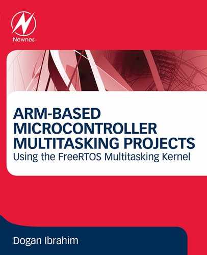
The basic features of the STM32F407VGT6 microcontroller are summarized in Fig. 2.1.
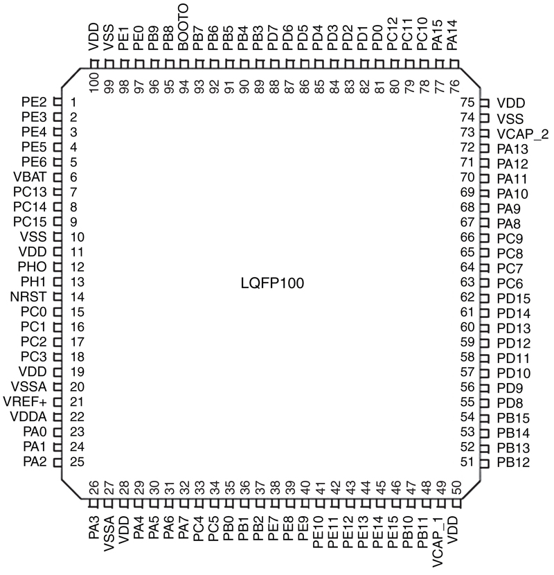
The internal block diagram of the microcontroller is shown in Fig. 2.3. At the top left corner is the 168 MHz Cortex-M4 processor with flash memory and SRAM, with DMA channels, USB and Ethernet modules just below the processor. The camera interface, voltage regulator, and external crystal inputs are shown at the top right-hand corner of the figure. The internal AHB (advanced high-speed bus) bus has two sections AHB1 and AHB2. AHB1 is divided into 84 MHz high-speed bus APB2 (advanced peripheral bus 2) and 42 MHz low-speed bus APB1 (advanced peripheral bus 1). APB2 supports some timers, SPI bus, USARTs, and ADC channels. The low-speed APB1 bus supports some timers, USARTs, I2C bus, CAN modules, DAC, and the watchdog timer. Clocks to the GPIO ports are driven from the high-speed 168 MHz AHB1 bus in the middle of the figure. AHB2 bus drives the camera interface and the USB port. Memories are shown in the top middle part of the figure.
The microcontroller is powered from VDD pins with a voltage in the range of 1.8–3.6 V. VDDA is the external analog power supply for the ADC and some other parts of the chip. A minimum of 1.8 V must be applied to VDDA when the ADC converter is used. VDDA and VSSA can be connected to VDD and VSS, respectively. VBAT is the external battery voltage for the RTC, 32 kHz oscillator and backup registers when the VDD is not present. This voltage must be in the range 1.65–3.6 V.
2.3.4. Low power modes
The STM32F407VGT6 microcontroller can be operated in one of three modes in low-power operations:
Sleep mode: In this mode, the CPU is stopped but all peripherals continue to operate. The CPU wakes up when an interrupt occurs.
Stop mode: All clocks are stopped and this mode provides the lowest power consumption while retaining the contents of CPU registers and SRAM.
Standby mode: In this mode oscillators and the voltage regulator are switched off and thus it provides the lowest power consumption. All register contents and SRAM contents are lost (except for registers in the backup circuitry).
2.3.5. The clock circuit
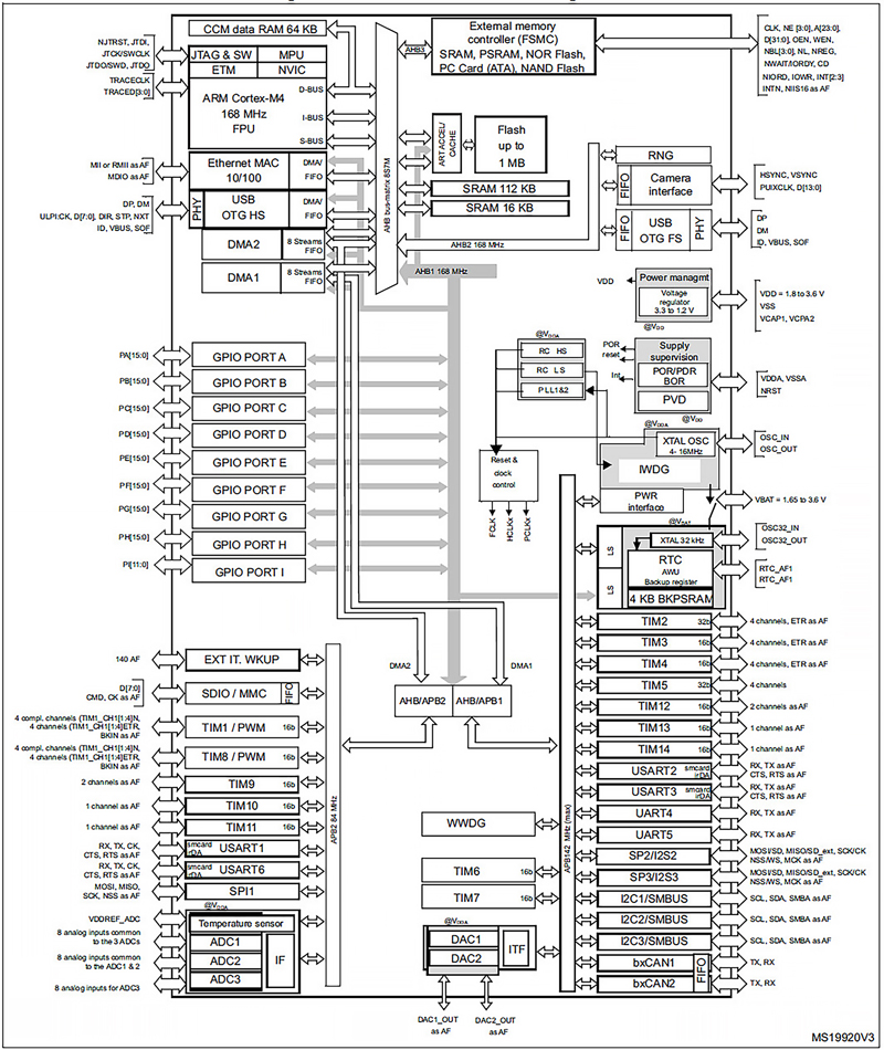
The clock circuit of the STM32F407VGT6 microcontroller is very powerful and at the same time very complex. Correct configuration of the clock circuit is very important as it controls all the timing within the microcontroller. In this section we shall be looking at the various clock options and also see how to configure the clock.
On reset, the 16 MHz internal RC oscillator is selected as the default CPU clock. The application program can then select either the RC oscillator or an external 4–26 MHz crystal-based clock source as the system clock. This clock can be monitored for failure and if a failure is detected, the system automatically switches back to the internal RC oscillator. This clock source is input to a PLL, thus allowing to increase the frequency up to 168 MHz. There are several prescalers that allow configuration of the clock for the required speed.
Basically, there are two types of clock sources that can be used to drive the system clock: external clock, and internal clock (Fig. 2.4).
Figure 2.4STM32F407VGT6 clock sources.
Fig. 2.5 shows the block diagram of the clock circuit.
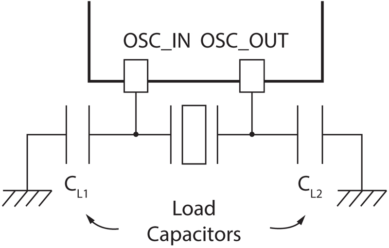
High-speed external (HSE): This can be an external crystal or resonator device, or an external clock signal. The frequency range of the crystal or resonator should be 4–26 MHz. Fig. 2.6 shows a typical crystal connection. It is recommended to use two capacitors in the range of 4–25 pF with the crystal circuit.
Figure 2.6Crystal oscillator connection.
When using a clock generator circuit, the waveform can be square, sine, or triangular and must be symmetrical, that is, 50% ON and 50% OFF times. The clock signal must be fed to the OSC_IN pin of the microcontroller (Fig. 2.7).
Figure 2.7Using clock generator circuit.
If external clock circuitry is used, the HSE oscillator should be bypassed to avoid any conflict.
Low speed external (LSE): This is a 32,768 Hz clock driven from an external crystal and feeding the internal real-time clock (RTC) module.
2.3.5.2. Internal clock sources
High-speed internal (HIS): This is an accurate 16 MHz internal clock with a factory-calibrated tolerance of 1%.
Low-speed internal (LSI): This clock source is not very accurate and is around 32 kHz. Although the LSI can be used to feed the RTC, it is not recommended as it is not very accurate. The LSI is normally used as a clock source for the independent watchdog (IWDG).
2.3.5.3. Configuring the clock
As shown in Fig. 2.5, the clock circuit consists of a number of multiplexers, prescalers, and a phase locked loop (PLL). The multiplexers are used to select the required clock source. The prescalers are used to divide the clock frequency by a constant. Similarly, the PLL is used to multiply the clock frequency with a constant in order to operate the chip at higher frequencies.
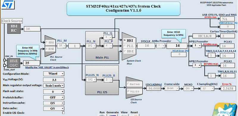
Configuring the clock by programming the internal clock registers is a complex task and detailed knowledge of the clock circuitry is required. Luckily, STMicroelectronics provides an Excel file tool to help configure the clock easily. Fig. 2.8 shows this Excel configuration tool (see web site: http://www.st.com/web/catalog/tools/FM147/CL1794/SC961/SS1533/PF257927#) in wizard mode. Using this tool one can easily configure the clock for the required speed.
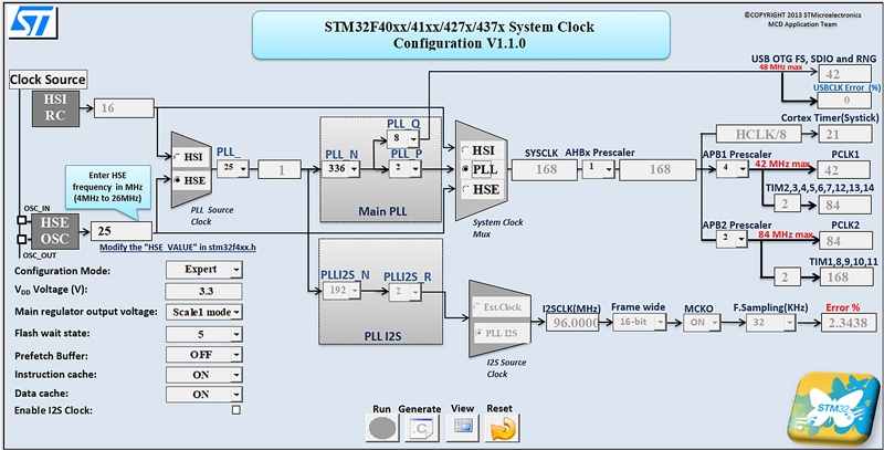
As an example, assuming that we are using an external 25 MHz crystal (this is the crystal used in the Clicker 2 for STM32 development board) and the required CPU clock is 168 MHz, the above Excel tool can be used in expert mode to find the various clock parameters. You should enable macros in excel and click the run button at the bottom of the display to configure the clock. The configuration settings for 168 MHz CPU clock are as follows (this is the settings used in all the projects in this book):
• Use HSE clock
• Set crystal frequency to 25 MHz
• Select HSE in the multiplexer
• Set PLL to 25
• Set PLL_N to 336
• Set PLL_P to 2
• Set PLL_Q to 8
• Select PLL
• Set AHBx prescaler to 1
As shown in Fig. 2.9, the CPU clock will be set to 168 MHz, APB1 clock to 42 MHz, and APB2 clock to 84 MHz.
Figure 2.9Configuring the clock.
2.4. General purpose inputs and outputs
General purpose inputs and outputs (GPIO) ports are arranged into five ports, each port 16-pin wide, and named as A, B, C, D, and E. Each port has a separate clock. Each port has the following basic features:
• Most of the port pins are +5V tolerable when used as inputs (except the analog input pins)
• Port outputs can be configured as push-pull, open-drain or pull-up, pull-down
• The speed of each port can be configured in software
• Port inputs can be configured as pull-up or pull-down, analog, or floating
• Port pins can be digital I/O or they can have alternative functions, such as DAC, SPI, USB, PWM, etc.)
• Each port pin can be used with one of 15 alternate functions (AF)
• Bit manipulations can be performed on each port pin
After hardware or software reset, the default values of the port pins are:
• Input
• Push-pull
• 2 MHz speed
• No pull-up or pull-down
Each I/O port has the following registers that can be programmed using the mikroC Pro for ARM language:
• 2 × 32-bit configuration registers GPIOx_CRL and GPIOx_CRH
• 2 × 32-bit data registers GPIOx_IDR and GPIOx_ODR
• 1 × 32-bit set/reset register GPIOx_BSRR
• 1 × 16-bit reset register GPIOx_BRR
• 1 × 32-bit locking register GPIOx_LCKR
Port pins can be individually configured by software in the following modes. Notice that the I/O port registers have to be accessed as 32-bit words:
• Input floating
• Input pull-up
• Input pull-down
• Input analog
• Output open-drain
• Output push-pull
• AF push-pull
• AF open-drain
Set/reset registers are used for read/modify accesses to any port pin without being interrupted by the system interrupt controller module.
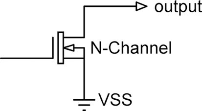
Fig. 2.10 shows the structure of a push-pull output port pin which is the most commonly used structure. Similarly, an open-drain output port pin is shown in Fig. 2.11. Input pull-up and pull-down circuits are shown in Fig. 2.12 and Fig. 2.13, respectively.
Figure 2.10Push-pull output pin.
Figure 2.11Open-drain output pin.
Figure 2.12Pull-up pin.
Figure 2.13Pull-down pin.
The basic structure of an I/O port pin is shown in Fig. 2.14. The push-pull transistors and pull-up and pull-down resistors can be seen from the figure. Notice that protection diodes are used at the port inputs to protect the input circuitry from high voltages.
Port configuration registers GPIOx_CRL and GPIOx_CRH are used to configure the following parameters of a port:
• Analog mode
• Floating input mode
• Input with pull-up/pull-down
• Output with push-pull
• Output with open-drain
• AF output with push-pull
• AF output with open-drain
• Output speed
Port data registers GPIOx_IDR and GPIOx_ODR are used to read and write data to a port respectively.
Port bit set/reset register GPIOx_BSRR or GPIOx_BRR are used in read/modify operations. Using these registers to modify a port pin protects the operation from interrupts. Thus, there is no need for the software to disable interrupts during port read/write operations.
Port locking register GPIOx_LCKR allows the input-output configuration of a port to be frozen until the microcontroller is reset. The locking operation is useful when the ports are configured and it is required to protect this configuration from accidental changes.
Port pins can be programmed for AF. For AF inputs, the port must be configured in the required input mode. Similarly, for AF outputs, the port must be configured in AF output mode. When a port is configured as an AF, the pull-up and pull-down resistors are disabled, the output is set to operate in push-pull or in open-drain mode.
Most of the port input pins are +5V tolerant which means that devices giving +5V outputs can directly be connected to the microcontroller input port pins without having to lower their voltages. A +5V tolerant input is shown as “FT” in data sheets.
2.5. Nested vectored interrupt controller (NVIC)
STM32F407 includes a nested vectored interrupt controller that can manage 16 priority levels and handle 82 maskable interrupts.
2.6. External interrupt controller (EXTI)
The external interrupt controller consists of 23 edge detected lines used to accept and generate interrupts. Each line can be configured independently to select the triggering mode as a rising edge, falling edge, or both, and each line can be masked individually under software control.
2.7. Timers
STM32F407 microcontroller includes two advanced-control timers, eight general purpose timers, two basic timers, and two watchdog timers. The timers have the following features:
3 × 12-bit ADC are included with each ADC sharing up to 16 external channels, each having 4096 levels of quantization. Conversion can be done as single-shot or in scan mode. Scan mode is the most commonly used option where automatic conversion is performed on the selected channels. Sample and hold functionality is available with the ADC channels which are used to hold the input signal just before a conversion takes place. The ADC can be triggered by any of TIM1, TIM2, TIM3, TIM4, or TIM8 timer.
2.9. Built-in temperature sensor
A built-in temperature sensor is provided on the microcontroller chip whose output voltage varies linearly with the chip temperature. The temperature sensor is internally connected to analog port ADC1_IN16. The temperature sensor is not accurate and can only be used to detect temperature changes instead of reading the absolute temperatures.
2.10. Digital-to-analog converter
2 × 12-bit DAC channels are provided with 8-bit or 12-bit outputs, offering 256 or 4096 levels of quantization. The converted data can be aligned left or right and each channel has DMA capability. The DAC channels additionally feature noise-wave generation or triangular-wave generation.
2.11. Reset
There are three types of reset: system reset, power reset, and backup domain reset. A system reset sets all registers to their default reset values. This reset is generated by one of the following events:
• Low-level signal on NRST pin (external reset)
• Watchdog timeout
• Software reset
• Low-power management reset
Low-power management reset is triggered when entering the Standby mode or when entering the Stop mode.
Power reset is generated when power is applied to the microcontroller or when exiting the Standby mode. Backup domain reset sets all RTC registers to their reset values. This type of reset is generated when a software reset is triggered by setting a bit in the backup domain control register, or if VDD or VBAT become ON if they were both previously OFF.
2.12. Electrical characteristics
It is important to know the absolute maximum and typical ratings of a microcontroller before it is used in a project. Stresses above the absolute maximum ratings for extended periods may affect device reliability and may even damage the device. Some of the absolute maximum ratings of the STM32F407VCT6 microcontroller are shown in Table 2.3. Notice from this table that the output current sunk and sourced by any I/O pin is specified as maximum 25 mA (the typical value is 8 mA, but for relaxed I/O voltages this current can be increased to 20 mA) and thus, direct LED drive is possible. To drive larger loads, it will be necessary to use BJT- or MOSFET-based transistor switching circuits or even relays for higher voltages. The total current sourced from all I/O pins plus the run consumption of the CPU should not exceed 240 mA. Care should be taken when driving CMOS circuits that operate with +5V since the output voltage of an I/O pin of the microcontroller will not be high enough to drive a CMOS input, even with pull-up resistors. In such circumstances it is recommended to use 3–5 V level converter circuits, for example, transistor switches or voltage converter integrated circuits.
Table 2.3
Absolute maximum ratings.
Symbol
Description
Absolute maximum ratings
Vdd-Vss
External supply voltage
4.0 V
Vin
Input voltage on +5V tolerant pin
Vdd + 4.0
Vin
Input voltage on non +5V tolerant pin
4.0 V
Ivdd
Total current into Vdd power lines (source)
240 mA
Ivss
Total current out of Vss ground lines (sink)
240 mA
Io
Output current sunk by any I/O pin
25 mA
Io
Output current sourced by any I/O pin
25 mA
Tstg
Storage temperature
−65°C to +150°C
Tj
Maximum junction temperature
150°C
Table 2.4 shows the typical operating conditions of the STM32F407VCT6 microcontroller. The values given in this table should be considered in normal operating conditions.
Table 2.4
Typical operating conditions.
Symbol
Description
Min
Max
fhclk
Internal AHB clock frequency
0
168 MHz
fpclk1
Internal APB1 clock frequency
0
42 MHz
fpclk2
Internal APB2 clock frequency
0
84 MHz
Vdd
Operating voltage
1.8 V
3.6 V
Vdda
ADC operating voltage
1.8 V
3.6 V
VBAT
Backup voltage
1.8 V
3.6 V
Pd
Power dissipation (LQFP100 package)
–
465 mW
Id
Supply current in Run mode, code in flash (at 168 MHz with all peripherals enabled)
–
87 mA
Id
Supply current in Run mode, code in flash (at 168 MHz with all peripherals disabled)
–
40 mA
2.13. Summary
In this chapter the basic features of the Cortex-M processors have been described. In addition, the architecture of the STM32F407VCT6 microcontroller has been described in some detail since this is the microcontroller that is used in all the projects in this book. The clock configuration options and general purpose input-output structure of the STM32F407VCT6 microcontroller are given in this chapter.
In the next chapter we shall be looking at the basic features of some of the commonly used ARM Cortex based development boards.