
6
Differential Phase Shift Keying Photonic Systems
This chapter investigates differential phase shift keying (DPSK) modulation for noncoherent transmission and detection optical communications systems. The differential mode of detection is most appropriate for such systems in which the phases contained in the two consecutive bit periods are assigned discrete values, for example, 0, π or 0, π/2, π and 3π/2. An experimental demonstration of DPSK modulation formats is also described.
6.1 Introduction
Owing to the tremendous growing demand for high-capacity transmission over the Internet, a high data rate of 40 Gbps per channel is an attractive feature of the next generation of lightwave communications system. Under the current 10 Gbps DWDM optical system, overlaying 40 Gbps on the existing network can be considered to be the most cost-effective method for upgrading purposes. However, there are a number of technical difficulties faced by communications engineers involving interoperability that requires a 40 Gbps line system to have signal optical bandwidth, tolerance to chromatic dispersion, resistance to nonlinear crosstalk, and susceptibility to accumulated noise over multispan of optical amplifier to be similar to a 10 Gbps system.
In view of this, advanced modulation formats have been demonstrated as an effective scheme to overcome 40 Gbps system impairments. The DPSK modulation format has attracted extensive studies owing to its benefit over conventional on–off keying (OOK) signaling format, including a 3 dB lower optical signal-to-noise ratio (OSNR) [1] at a given bit error rate (BER), more robust to narrow band optical filtering, and even more robust against some nonlinear effects such as cross-phase modulation and self-phase modulation. Moreover, spectral efficiencies can be improved by using multilevel signaling. On top of that, coherent detection is not critical as DPSK detection requires comparison of two consecutive pulses, and hence the source coherence is required only over one-bit period.
Nevertheless, the DPSK format involves rapid phase change, which causes intensity ripples due to chromatic dispersion that induce a pattern-dependent SPM-GVD (group velocity dispersion) effect [2]. Therefore, a return-to-zero (RZ) pulse can be employed in conjunction with DPSK to generate more tolerance to the data-pattern-dependent SPM-GVD effect. In addition, RZ improves dispersion tolerance and nonlinear effects, particularly in long-haul networks at high data rates. Specific RZ formats such as carrier-suppressed RZ (CSRZ) help to reduce the inherent wide spectral bandwidth.
At 40 Gbps, generation of RZ pulses is not feasible as it is at 10 Gbps owing to the large band-width requirement. Thus, 40 Gbps RZ signals are produced optically in a “pulse carver” by driving the modulator with a 20 GHz RF signal. With the remarkable advances in external modulator, especially the Mach–Zehnder interferometric (intensity) modulator (MZIM), this is easily achieved by utilizing the microwave optical transfer characteristic of the MZIM.
Despite the telecom boom and subsequent bust, Internet traffic has been steadily growing. This growth requires new investment in telecommunications infrastructure to provide long-haul communications capacity between major population centers in the world. The transmission route between Melbourne to Sydney and vice versa, for example, is one of the most intensive, demanding upgradation to higher capacity, especially from the current 10–40 Gbps. One of the most cost-effective ways to provide such upgrades is to use the existing fiber infrastructure, and upgrade the transmitters and receivers at either end of the long-haul-links. That implies a transmission rate of 40 Gbps over the existing 10G RZ format dense multiwavelength optical communications systems.
Because of the properties of the installed fiber (which is older and also more degraded than the state-of-the-art fibers used in laboratory “hero” experiments), the transmission methods must be highly tolerant to chromatic dispersion (CD) and polarization-mode dispersion (PMD). This favors the use of advanced modulation formats (such as variants of phase shift keying) rather than ultra-high-rate time division-multiplexed (TDM) schemes, because the effects of CD and second-order PMD are proportional to the square of the bit rate. However, there are various optical filters installed throughout DWM optical transmission systems such as optical multiplexers (muxes), demultiplexers (demuxes), and add-drop muxes that would affect the spectral properties of the multiplexed channels, particularly for a hybrid transmission of 10 Gbps and 40 Gbps channels.
Recently, advanced modulation formats are considered to play a significant role in enhancing the effectiveness of bandwidth reduction and effective transmission over long distances [1,2]. These advanced modulation formats are new to optical communications but are very well known in wire and wireless communications systems. Accordingly, the modulation can manipulate the amplitude, the frequency, or the phase of the carriers corresponding to the coding of the input data sequence. Either coherent or incoherent transmission and detection techniques have been employed over the years for optical systems. However, incoherent detection is preferred so as to minimize the linewidth obstacles of the lasers at the transmitter and the local oscillators required for homodyne or heterodyne coherent detection systems. Furthermore, the phase comparison in differential detection can be easily implemented using delay interferometric photonic components. If such phase comparison is implemented in the electrical domain operating at high bit rate, it is quite difficult. Therefore, differential, discrete, or continuous phase modulation formats can be the preferred techniques.
This chapter investigates the transmission of 40 Gbps channels over 10 Gbps DWDM optical system in which “standard” single optical filters (SSMFs) normally employed for 10 Gbps systems are used. DPSK is transmitted and compared with those employing RZ- and NRZ-amplitude shift keying (ASK). We demonstrate that with the passband of optical filters on the order of 0.5 nm, the transmitted 40 Gbps channels are not penalized and vice versa for 10 Gbps DWDM channels. Transmission BER and receiver sensitivities are reported for different transmission scenarios.
Owing to the high demand for data transmission capacity, with the advent of wavelength division multiplexing (WDM) technology, data transmission has reached a revolutionary stage for increasing higher system capacity. Higher bit rates up to 40 Gbps and growing numbers of WDM channels are increasingly challenging the limit of the ASK format.
6.2 Optical Dpsk Modulation and Formats
Figure 6.1 shows the structure of a 40 Gbps DPSK transmitter in which two external LiNbO3 optical interferometric modulators (MZIMs) are used [3].
The operational principles of MZIMs were presented in Chapter 2. The MZIM used in Figure 6.1 can be either a single- or a dual-drive type. As previously described, the optical DPSK transmitter consists of (i) a narrow-linewidth laser source to generate a lightwave of a wavelength that conforms to the ITU grid, (ii) two cascade MZIMs are employed to modulate the lightwaves, one to generate a periodic (clock-like) return zero or CSRZ formats and the differential phase of the lightwave and one data modulator switching on and off the optical clock sequence. This shift can be continuous between the states as in the case of continuous phase FSK or minimum shift keying modulation formats, which will be presented in later chapters.
6.2.1 Generation of RZ Pulses
The first MZIM, commonly known as the pulse carver, is used to generate the periodic pulse trains with the required RZ format. The suppression of the lightwave carrier can also be carried out at this stage if necessary and is known as carrier-suppressed RZ (CSRZ). The CSRZ pulse shape has been found to have attractive attributes in long-haul WDM transmissions compared to other RZ types, including an optical phase difference of π in adjacent bits, suppression of the optical carrier component in the optical spectrum, and smaller spectral width. Figure 6.2 shows the structure of a 40 Gbps ASK transmitter in which two external LiNbO3 optical interferometric modulators (MZIMs) [4] are used. The operational principles of MZIMs were presented in Chapter 2. The MZIM used in Figure 6.2 can be either a single- or dual-drive type. The optical ASK transmitter would consist of a narrow-linewidth laser source to generate a lightwave of wavelength conforming to the ITU grid.
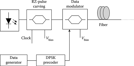
FIGURE 6.1 Schematic diagram of a discrete PSK optical transmitter using cascaded MZI modulators.
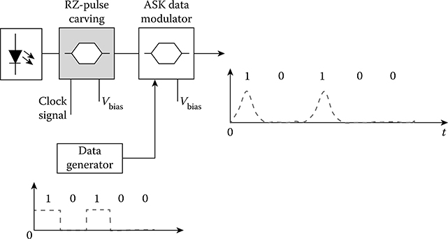
FIGURE 6.2 Cascaded MZIM for generation of RZ or CSRZ-DPSK lightwave signals.
Different types of RZ pulses can be generated depending on the driving amplitude of the RF voltage and the biasing schemes of the MZIM. The equations governing the RZ pulses electric field waveforms are [1]
where Eb is the pulse energy per transmitted bit.
The first type of pulse, the 33% duty-ratio RZ pulse, is commonly known as the “carrier max or conventional” (RZ33) pulse, whereas the 67% duty cycle RZ pulse is the CSRZ pulse type. The difference in the generation between these two RZ pulse types is due to different biasing point placed on the transfer curve of the MZIM. The bias voltage conditions and the pulse shape of these two RZ types, the carrier suppression and nonsuppression of the maximum carrier, can be implemented with the biasing points at the minimum and maximum transmission points of the transmittance characteristics of the MZIM, respectively. The peak-to-peak amplitude of the RF driving voltage is 2Vπ, where Vπ is the required driving voltage to achieve a π phase shift of the lightwave carrier. Another important point is that the RF signal is operating at only half of the transmission bit rate. Hence, pulse carving is actually implementing the frequency doubling. The generation of RZ33 and CSRZ pulse trains is shown in Figure 6.3a and b.
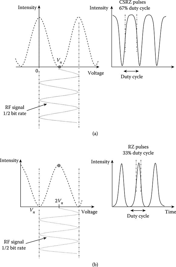
FIGURE 6.3 Biasing and driving sinusoidal electrical waveform to generate (a) CSRZ and (b) RZ33 (pulse width occupies 33% pulse period).
The pulse carver can also utilize a dual-drive MZIM, which is driven by two complementary sinusoidal RF signals. This pulse carver is biased at –Vπ/2 and +Vπ/2 with a peak-to-peak amplitude of Vπ/2. Thus, a π phase shift is created between the states 1 and 0 of the pulse sequence and hence the RZ with alternating phases 0 and π. If carrier suppression is required, then the two electrodes are supplied voltages Vπ with a swing voltage amplitude of Vπ.
RZ optical systems are proved to be more robust against impairments, especially self-phase modulation and PMD. Although RZ modulation offers improved performance, RZ optical systems usually require more complex transmitters than those in the NRZ ones. Compared to only one stage for modulating data on the NRZ optical signals, two modulation stages are required for the generation of RZ optical pulses.
6.2.2 Phasor Representation
Recalling the derivation of a phase-modulated interferometer given in Chapter 2, we see that the output field of the MZIM is given by
It can be seen that the modulating process for the generation of RZ pulses can be represented by a phasor diagram as shown in Figure 6.4. This technique gives a clear understanding of the super-position of the fields at the coupling output of the two arms of the MZIM. Here, a dual-drive MZIM is used, that is, the data [V1(t)] and the complementary data are applied to each arm of the MZIM, and the RF voltages swing in inverse directions. Applying the phasor representation, vector addition, and simple trigonometric calculus, the process of generation of RZ33 and CSRZ is explained in detail and verified.
The width of these pulses is commonly measured at the position of full-width half maximum (FWHM). Note that the measured pulses are intensity pulses, whereas we are considering the addition of the fields in the MZIM. Thus, the normalized E0 field vector has the value of at the FWHM intensity pulse positions, and the time interval between these FWHM points gives the FWHM values.
6.2.3 Phasor Representation of CSRZ Pulses
Key parameters, including the Vbias, the amplitude of driving voltage, and its corresponding initialized phasor representation, are shown in Figure 6.5a and b, respectively.
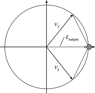
FIGURE 6.4 Phasor representation for generation of output field in dual-drive MZIM.
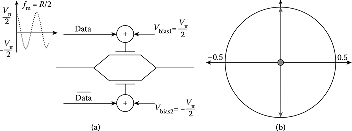
FIGURE 6.5 Biasing voltages of (a) MZIM structure and (b) phasor representation for RZ pulse generation.
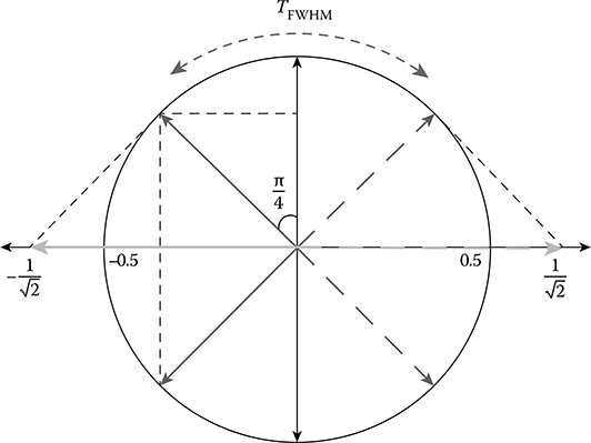
FIGURE 6.6 Phasor representation of evolution of CSRZ pulse generation using dual-drive MZIM.
The swing voltage of the driving RF signal on each arm has the amplitude of Vπ/2 (i.e., Vp−p = Vπ). The RF signal operates at half of the bit rate (BR/2). At the FWHM position of the optical pulse, and the component vectors V1 and V2 form with the vertical axis a phase of π/4 as shown in Figure 6.6.
Considering the scenario for the generation of 40 Gbps CSRZ optical signals (25 ps pulse width), the modulating frequency is fm = 20 GHz. = BR/2. At the FWHM positions of the optical pulse, the phase is given by the following expressions
Thus, the calculation of the TFWHM can be carried out, and hence the duty cycle of the RZ optical pulse can be obtained as given in the following expressions
The result clearly verifies the generation of CSRZ optical pulses.
6.2.4 Phasor Representation of RZ33 Pulses
Key parameters, including Vbias, the amplitude of the driving voltage, and its corresponding initialized phasor representation, are shown in Figure 6.7a and b, respectively.
At the FWHM position of the optical pulse, and the component vectors V1 and V2 form with the horizontal axis a phase of π/4 as shown in Figure 6.8.
Considering the scenario for generation of a 40 Gbps CSRZ optical signal (25 ps pulses), the modulating frequency fm = 20 GHz = BR/2. At the FWHM positions of the optical pulse, the phase is given by the following expressions
Thus, the calculation of TFWHM can be carried out, and hence the duty cycle of the RZ optical pulse can be obtained as given in the following expressions
Therefore, the result clearly verifies the generation of RZ33 optical pulses.
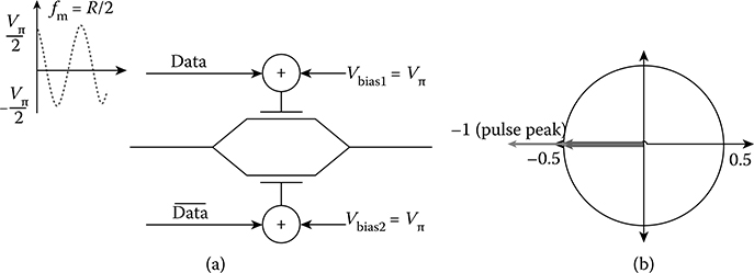
FIGURE 6.7 (a) Optical scheme for generation of 33% RZ lightwave pulse sequence. (b) Phasor representation of the generation. Vbias is Vπ for both arms, Swing voltage of driving RF signal on each arm has the amplitude of Vπ/2 (i.e Vp-p = Vπ) and RF signal operates at half of bit rate (R/2).
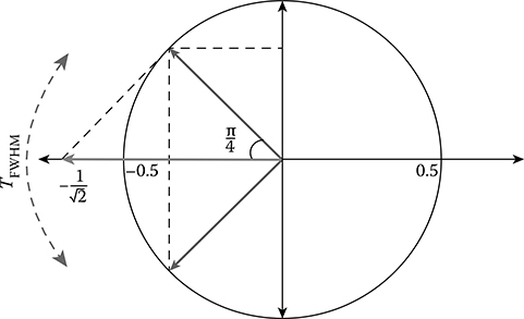
FIGURE 6.8 Phasor representation of RZ33 pulse generation using dual-drive MZIM.
6.2.5 Discrete Phase Modulation—DPSK
6.2.5.1 Principles of DPSK and Theoretical Treatment of DPSK and DQPSK Transmission
For PSK signals, the data information is contained in the discrete phase shifts relative to the phase of the unmodulated carrier. The required absolute phase at the receiver must be supplied by the recovered carrier such as the OPLL or relatively the electrical PLL, which would be complicated. Thus, it is more effective to process the phase difference of the two consecutive symbols.
Information encoded in the phase of an optical carrier is commonly referred to as optical phase shift keying. In the early days, PSK required precise alignment of the transmitter and demodulator center frequencies. Hence, the PSK system was not widely deployed. With the introduction of the DPSK scheme, coherent detection is not critical because DPSK detection only requires source coherence over one-bit period by a comparison of two consecutive pulses.
A binary 1 is encoded if the present input bit and the past encoded bit are of opposite logic, and a binary 0 is encoded if the logic is similar. This operation is equivalent to the XOR logic operation. Hence, an XOR gate is usually employed in the differential encoder. A NOR operation can also be used to replace the XOR operation in differential encoding, as shown in Figure 6.9a. The decoding logic circuit is also shown in this figure.
In optical applications, electrical data 1 is represented by a π phase change between the consecutive data bits in the optical carrier, whereas state 0 is encoded with no phase change between the consecutive data bits. Hence, this encoding scheme gives rise to two points located exactly at a π phase difference with respect to each other in the signal constellation diagram. For continuous phase shift keying such as minimum shift keying, the phase evolves continuously over a quarter of the section, and thus a phase change of π/2 between one state and another [5] as indicated by the bold circles shown in Figure 6.9b.
For differential quadrature phase shift keying (DQPSK), another quadrature component or subsystem would be superimposed on the DPSK (the in-phase) such that they are orthogonal to each other. In other words, the phase constellation of Figure 6.9b would have another imaginary (π/2) axis with the states +π/2 and –π/2.
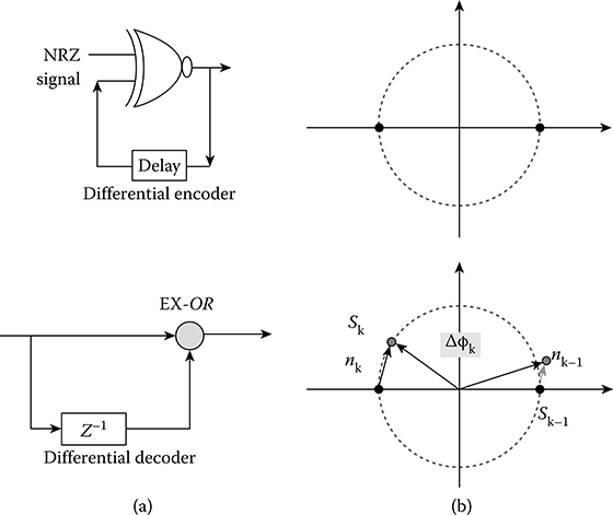
FIGURE 6.9 (a) DPSK precoder and decoder for encoding and decoding of differential data and (b) signal constellation diagram of phasor representation.
6.2.5.2 Optical DPSK Transmitter
Figure 6.10 shows the structure of a 40 Gbps DPSK transmitter in which two external LiNbO3 optical interferometric modulators [3] (MZIMs) are used. The operational principles of MZIMs were presented in Chapter 2. The MZIM used in Figure 6.10 can be either a single-or dual-drive type. The optical DPSK transmitter would consist of a narrow-linewidth laser source to generate a lightwave of wavelength conforming to the ITU grid.
As shown in Figure 6.11, the optical RZ pulses are then fed into the second MZIM through which the RZ pulses are modulated by the precoded NRZ binary data to generate RZ-DPSK optical signals. Electrical data pulses are differentially precoded in the precoder using the XOR coding scheme. Without the pulse carver and the sinusoidal RF signal, the system becomes an NRZ-DPSK transmitter.
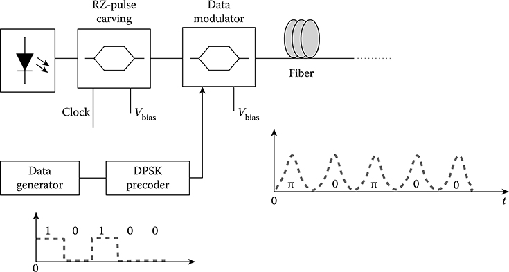
FIGURE 6.10 Generation of RZ formats DPSK modulation.
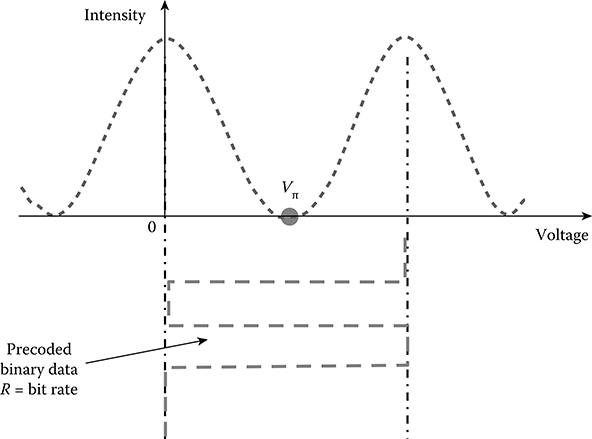
FIGURE 6.11 Voltage bias and amplitude swing levels for NRZ-DPSK modulation formats.
In DPSK modulation, the MZIM is biased at the minimum transmission point. The precoded electrical data have a peak-to-peak amplitude equal to 2Vπ and operate at the transmission bit rate. The modulation principles are demonstrated in Figure 6.11.
An electro-optic phase modulator (PM) might also be used for the generation of DPSK signals, but the Mach–Zehnder wave guide structure has several advantages over the PM described in Ref. [1]. Using an optical PM, the transmitted optical signal is chirped, whereas using an electro-optic intensity modulator (MZIM, especially X-cut versions), chirp-free signals are produced. In practice, a small amount of chirp might be useful for transmission [6].
6.2.6 DPSK-Balanced Receiver
Consider two consecutive symbols whose signals can be represented by
where A is an arbitrary amplitude and fc the carrier frequency. At the receiver side, the phase difference Δφk = φk−φk−1 has to be determined. If there is no distortion, then the phase difference is that of the original phase difference generated at the transmitter. However, in general, the signals are distorted when reaching the receiver, and thus we have
Figure 6.9b shows the position of the data signals at the receiver side, including the additional contribution of the noise vectors of the two consecutive intervals. The phase angle between the two vectors can then be written as
representing the scalar products between the two received signal vectors xk and xk−1. For the non-distortion case of the binary DPSK modulation format, the phase difference would be 0 and π; thus, Δπk = π. Thus, the received signals are in push–pull states, hence the phase difference is bipolar. Equation 6.8 can then be reinterpreted as
The receiver for determination of the differential phase can be implemented using a balanced receiver operating in the push-pull mode. The delay balanced receiver is shown at the left side in Figure 6.12, in which the received optical field is split into two arms, one delayed in the optical domain by a symbol period and the other with no delay. The delay time must be matched to the propagation time of the lightwave carrier over the guided region of the optical fiber or integrated waveguide. A thermal tuning section is normally used to adjust to any mismatched time delay section. Two photodetectors are connected in a balanced configuration, producing the push-pull eye diagram (Equation 6.10) as shown in Figure 6.12b.
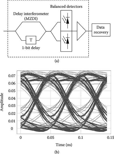
FIGURE 6.12 Schematic diagram of the balanced receiver for detection of the phase difference of two consecutive bits: (a) structure and (b) a sample of phase detected eye diagram. Bit rate = 20 Gbps format RZ.
Figure 6.12 shows the structure of an MZ delay interferometer (MZDI)-based DPSK-balanced receiver with an insert of a typical eye diagram at the output of the MZDI-balanced receiver for 50 ps, that is, 20 Gbps DPSK optical pulses. Note that the diagram shown is of a RZ format so there is no continuous baseline. The received signal at the output of the balanced receiver is given as [7]
where ED(t) and ED(t − τ) are the current and the one-bit delay version of the optical DPSK pulses, respectively. Δϕ and ς represent the differential phase and the phase noise caused by the MZDI imperfections. The latter issue is not a serious degradation factor in modern MZDI-based DPSK receivers owing to the use of a thin-film heater for tuning any waveguide path mismatch. The tuning has high stability with the implementation of the electronic feedback control circuit.
6.3 Dpsk Transmission Experiment
6.3.1 Components and Operational Characteristics
The components and features of the optical transmission system shown in Figure 6.13 for ASK and DPSK modulation and related formats of RZ, NRZ, and CSRZ are given in Table 6.1.
6.3.2 Spectra Of Modulation Formats
The center wavelength is set at 1551.72 nm. The experimental spectra of NRZ, RZ, and CSRZ of the ASK and DPSK formats are shown in Figure 6.14. Note that for DPSK spectra, the carrier at the center is at the same level as that of the signal. The RZ spectra are wider than that of the NRZ as expected owing to the shorter pulse width. The influence of the spectra of the optical signals on the dispersion and nonlinear impairments will be discussed in Section 6.5.2. For CSRZ, the carrier is clearly suppressed. Owing to the resolution of the spectrum analyzer, deep suppression is not observed.
6.3.3 Dispersion Tolerance of Optical DPSK Formats
A typical experimental test bed is set up as shown in Figure 6.15.
There are significant points for consideration in the setup of the test bed: (1) 40 Gbps Tx is the SHF 5003 DPSK transmitter, which can generate both ASK and DPSK data; (2) in the case of ASK, the Lab Buddy optical receiver (45 GHz with built-in amplifier) is used; (3) in the case of DPSK, the SHF 5008 DPSK receiver is used (MZ—one-bit delay); also, the electrical amp is utilized to drive the error analyzer; (4) a JDS 1.2 nm filter was utilized after EDFA to decrease the ASE noise level; and (v) power launched into the SMF (right after the transmitter Tx) is low, and hence nonlinearities do not have any impact. The launched power is recorded as shown in Table 6.2.
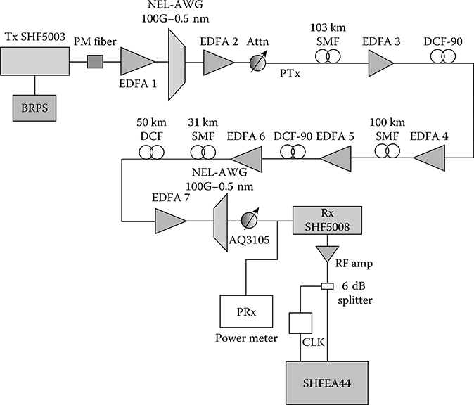
FIGURE 6.13 Experiment setup for evaluation of modulation formats of ASK and DPSK modulation, 230 km three optically amplified spans transmission, 234 km SMF and 230 km DCF.
TABLE 6.1
Photonic Components and Operating Characteristics
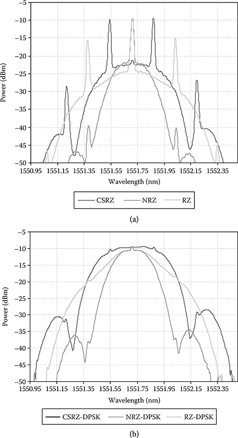
FIGURE 6.14 Optical spectra of transmitted optical signals of formats NRZ, RZ, and CSRZ for (a) ASK and (b) DPSK.
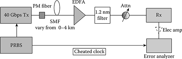
FIGURE 6.15 Experimental test bed for investigation of dispersion tolerance of transmission system.
Using a directly derived clock, that is, directly from the bit pattern generator and hence without the clock recovery unit, the error analyzer directly uses the clock pulse of the PRBS. The laser source center wavelength is set at 1551.72 nm, and the pulse pattern of PRBS is 231 − 1. Figures 6.16 and 6.17 depict the eye diagrams at the receiver under back-to-back connection and transmission over a distance of SSMF without dispersion compensating under modulation formats DPSK and ASK using self-homodyne reception. Figure 6.18 shows the performance of CSRZ/RZ/NRZ-DPSK formats over lengths of 0 – 4 km (from top down to bottom) of SSMF using the eye diagrams of 40 Gbps transmission. Hence, dispersion tolerance to the transmission fiber SSMF with a dispersion factor of D = +17 ps/(nm · km) for the DPSK format versus the conventional ASK format can be obtained.
TABLE 6.2
Maximum Power Launched into input of the Optical Fiber Transmission for Different Modulations ASK and DPSK with RXZ, NRZ, and CSRZ Formats
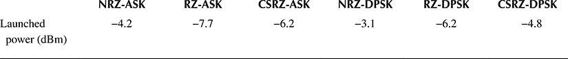
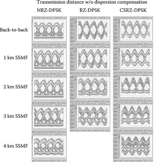
FIGURE 6.16 Eye diagrams of DPSK transmission after 0, 1, 2, 3, and 4 km SSMF for evaluation of the dispersion tolerance.
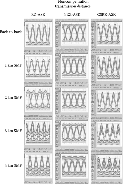
FIGURE 6.17 Eye diagrams of ASK transmission after 0, 1, 2, 3, and 4 km SSMF for evaluation of the dispersion tolerance of the transmission system.
It can be seen clearly that the DPSK system offers an improvement of approximately 3 dB in receiver sensitivity compared to the same ASK system. The obtained results confirm the theoretical analysis (Figure 6.19).
6.3.4 Optical Filtering Effects
Initially, the impacts of the optical filtering characteristics of the mux are evaluated using a back-to-back setup as shown in Figure 6.20. We set the sampling clock directly from the auxiliary clock output of the 231 − 1 pattern generator. Although two AWGs can be used as muxes and demuxes, we use only one AWG at either the transmitter or receiver sites. The other filter can be substituted with a multilayer thin-film optical filter. Two optical filters acting as mux and demux at the transmitting and receiving ends are then used to evaluate their impacts on 40 Gbps channels. We observe no significant degradation of the BER as shown in Figure 6.21.
Figure 6.22 shows the BER versus the receiver sensitivity curves obtained for ASK, and DPSK and DQPSK with RZ, NRZ, or CSRZ formats are shown in Figure 6.21. The sensitivities do not change significantly under the influence of the 0.5 nm optical filter on 40 Gbps channels operating under different modulation formats. We can now observe the optical spectra of ASK and PSK formats as shown in Figure 6.1a and b. The Gaussian-like or cos2 profile of the pulses generated at the output of both optical modulators and the parabolic passband properties of the AWG can tolerate a wide signal spectrum. We do not observe any degradation of the BER versus the sensitivity for the cases of wideband optical filters (1.2 nm) and 0.5 nm optical mux filtering. The detected eye diagrams under RZ- and CSRZ-DPSK transmission are shown in Figure 6.16. The MZDI acting as a phase comparator is thermally tuned so as to obtain a maximum eye opening, and thus an optimum BER.
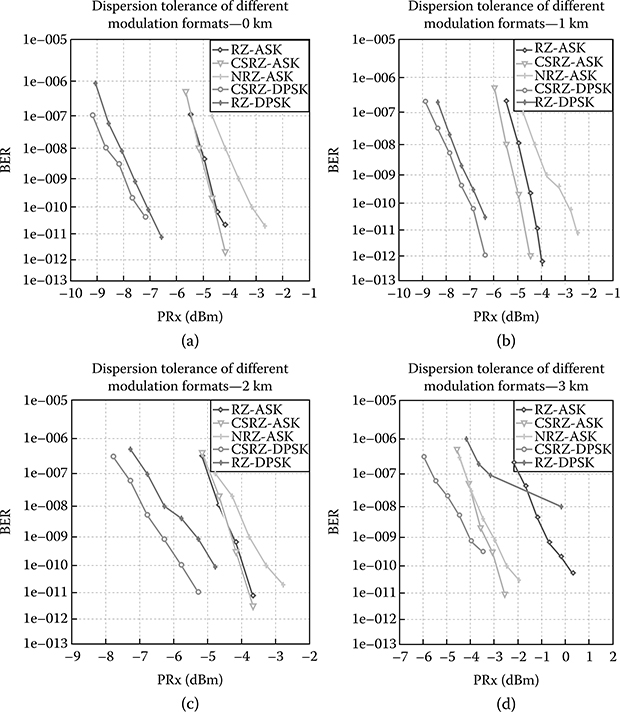
FIGURE 6.18 Performance of dispersion tolerance of advanced modulation formats in the case of (a) back to back (b) 1 km (c) 2 km; and (d) 3 km of SSMF residual length.
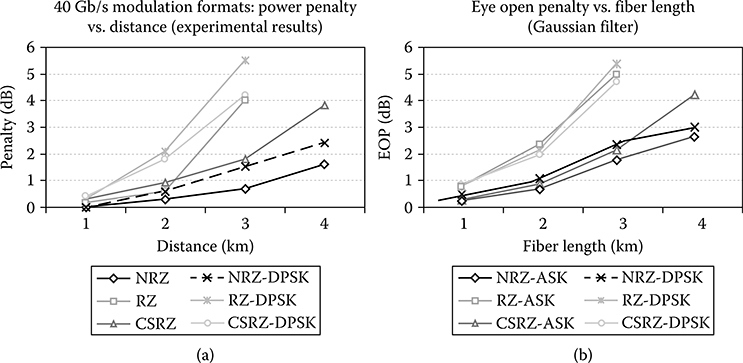
FIGURE 6.19 (a) Experimental results and (b) simulation results on power penalties induced chromatic dispersion limits of ASK and DPSK formats.
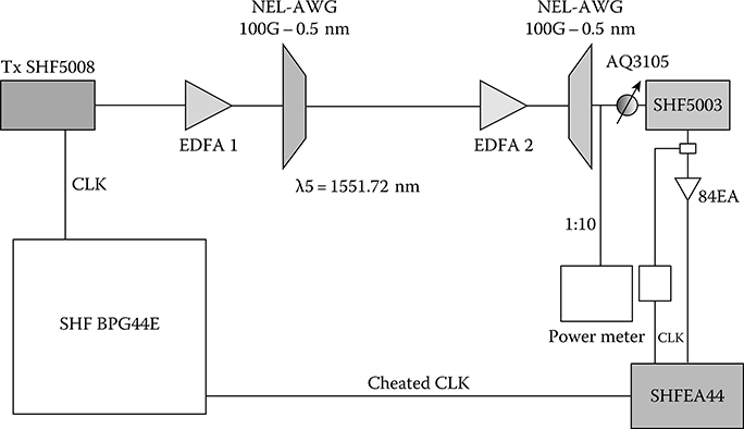
FIGURE 6.20 Back-to-back experimental system for investigation of the optical AWG filtering impacts on modulation formats.
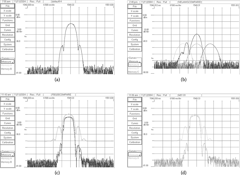
FIGURE 6.21 Optical passbands of AWG filters. (a) Top-left corner: signal spectrum of a channel. (b) Top-right corner: optical passbands of the multiplexed output of the AWG. Note the parabolic passband character-istics and the “black” curve of the output spectra of a wavelength channel. (c) Signal spectrum and its output of the AWG. (d) Same as (c) but a different wavelength region.
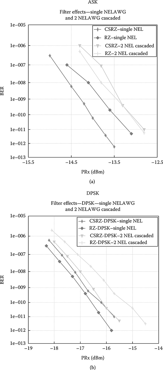
FIGURE 6.22 BER versus input power level of (a) ASK and (b) DPSK modulation with various formats.
The characteristics of multiplexers/demultiplexers that are currently utilized for 10 Gbps systems still offer sufficiently good performance for 40 Gbps transmission systems. The experimental results suggest the feasibility of upgrading the currently deployed system to a higher transmission rate: 40 Gbps. A higher bit rate such as 80 or 160 Gbps needs to be further investigated.
6.3.5 Performance of CSRZ-DPSK Over a Dispersion-Managed Optical Transmission Link
A dispersion-managed optical transmission link over 328 km length is set up as shown in Figure 6.13 with three optically amplified spans. The dispersion factor of the transmission fiber is matched with that of a length of dispersion compensation fiber. The bit pattern generator (BPBG) is used to drive the modulators of the transmitter. RZ and CSRZ can also be generated by a signal synthesizer. The nonlinear effect is explored by varying the optical power launched into the SMF from 0 to 15 dBm as shown in Figure 6.23. The power launched into the dispersion-compensating fiber (DCF) is kept unchanged at 0 dBm (nonlinearities are generated in SMF, not DCF).
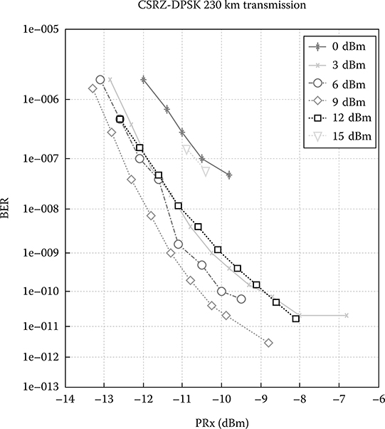
FIGURE 6.23 Transmission performance of CSRZ-DPSK under different power launched levels.
Note that mopping up of the residual dispersion using a tunable dispersion compensator is used and set at the wavelength 1555.75 nm, which can be shown to be optimum compared with the BER performance curve obtained at λ5 = 1551.72 nm. Hence, the laser source is tuned to this wavelength.
6.3.6 Mutual Impact of Adjacent 10G and 40G Dwdm Channels
A 320 km transmission is also conducted to assess the performance of 10G NRZ-ASK and a CSRZ-DPSK 40G channel. The transmission of adjacent and nonadjacent channels is demonstrated and evaluated with a 100 GHz AWG mux and a 1.2 nm tunable filter at the input of the Rx. An insignificant power penalty is observed when the adjacent 40G channel is co-transmitted. The setup of the transmission system is shown in Figure 6.24 which consists of (1) a 320 km SSMF and a dispersion-compensating module with two optical filters and splitters, (2) the optical transmitters, (3) 100 GHz AWG as optical multiplexers (at transmitter side) and demultiplexers (at the receiving side), and then (3) the optical reception subsystems. An optical filter is inserted at the front end to measure the impact of adjacent CSRZ-DPSK 40G channels on the 10G NRZ-ASK performance. No significant impact was noted when 4a 0G channel, adjacent or nonadjacent, was co-transmitted, as evaluated in Figure 6.25.
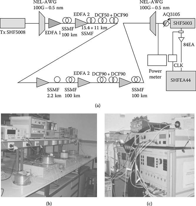
FIGURE 6.24 (a) Setup of the optically amplified long-haul optical transmission system: the span length can be varied for 50–320 km. (b) Optically amplified and dispersion-compensated fiber transmission line— transmitter and receiver plus (c) 40 Gbps bit pattern generator and error analyzer.
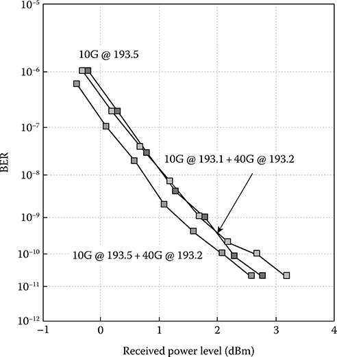
FIGURE 6.25 320 km transmission 40 impact on 10G channel: BER versus receiver sensitivity (dBm)— effects of 40G (CSRZ-DPSK) with 10G (NRZ-ASK) channel simultaneously transmitted for NRZ-ASK and CSRZ-DPSK formats—light gray dots for 1.2-nm-thin film filter and dark gray dots for 0.5-nm-thin AWG filter (demux with 100 GHz spacing).
6.4 Dqpsk Modulation Format
When digitizing data for transmission across many hundreds of kilometers, many digital modulaion formats have been proposed and investigated. This section investigates the DQPSK modulation format. This modulation scheme, although having been in existence for quite some time, has only been implemented in the electrical domain. Its application to optical systems proved difficult in the past as constant phase shifts in optical carriers (OCs) were required to be maintained. However, with the improvement of optical technology and alternative transmitter design setups, these difficulties have been eliminated.
6.4.1 Dqpsk
One of the main attractive features of the DQPSK modulation format is that it offers both twice as much bandwidth and increased spectral efficiency compared to OOK. As an example, comparisons between 8 × 80 Gbps DQPSK systems and 8 × 40 Gbps OOK systems show that DQPSK modulation offers more superior performance, that is, spectral efficiency. The very nature of the signaling process also makes noncoherent detection at a receiver feasible, thus reducing the overall cost of the system design.
As the name suggests, the idea behind the DQPSK modulation format is to apply a differential form of phase shift modulation to the optical carrier which encodes the data. DQPSK is an extension to the simpler DPSK format. Rather than having two possible symbol phase states (0 or π phase shift) between adjacent symbols, DQPSK employs a four-symbol equivalent {0, π/2, π, or 3π/2}. Depending on the desired dibit combination to be encoded, the difference in phase between the two adjacent symbols (optical carrier pulses) is varied systematically. Table 6.3 outlines this behavior.
The parameters φ1 and φ2 as indicated in Table 6.3 are the phases of adjacent symbols. The table can also be represented in the form commonly known as a constellation diagram (see Figure 6.26), which graphically explains the signal’s state in both amplitude and phase.
The DQPSK transmitter design is based on a design that was previously experimentally proposed [8]. First, we implement an RZ pulse carving MZM that generates the desired RZ pulse shape as described in Chapter 2. Next, an MZIM (generating 0 or π phase shift of the OC) is to be coupled along with a PM that induces a 0 or π/2 phase shift of the OC. When placed in this configuration, the four phase states of the OC required by the DQPSK modulation format, {0, π/2, π, or 3π/2}, can be achieved. Both the MZM and PM are to be driven by random binary generators operating at 40 Gbps. Figure 6.27 is a schematic of the system transmitters implementing RZ-DQPSK modulation. We originally started with the NRZ-DQPSK design; however, the RZ format is used more readily in practice and has proved to be more robust to system nonlinearities. The pulse sequence generated after the pulse carver is shown in Figure 6.28.
For DQPSK, the signal constellation can be considered to be two DPSKs orthogonal to each other. That is, there is a phase shift of π/2 between the constellation points. Thus, the transmitter and receiver can be implemented with the following phase difference
TABLE 6.3
DQPSK Modulation Phase Shifts
| Dibit | phase Difference Δϕ = ϕ2 ϕ1(degrees) |
| 00 | 0 |
| 01 | 90 |
| 10 | 180 |
| 11 | 270 |
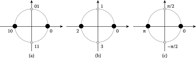
FIGURE 6.26 DQPSK signal constellation and assignment of phase symbols: (a) quarternary digits, (b) two-digit binary word, and (c) phase complex plane.
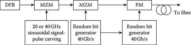
FIGURE 6.27 Schematic of a channel implementing RZ-DQPSK modulation.
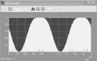
FIGURE 6.28 The optical carrier after RZ pulse carving using an MZM driven by a 10 GHz electrical signal.
In the latter case, the receiver simply outputs the binary bits of the imaginary and real parts of the DQPSK signals.
This can be explained as follows. The data information transmitted during the time interval [(k−1)Ts, kTs] with Ts as the symbol period is carried by the in-phase and quadrature components of the signal and thus given by the sign of the terms sin and cos as given in Equation 6.13. An offset of the signal constellation by π/4 would assist the simplification of the transmitter and receiver due to the fact that
Or effectively, there would be three output levels while the π/4 shift would give binary levels.
For the noiseless case, the correlation between the two bits is given as
The phase difference Δϕk = ϕk − ϕk−1 ∈ {0, π} leads to cos(Δϕk + Kπ) ∈ {1, −1}, ensuring the maximum distance between the two difference symbols.
In the rest of this section, some of the key principles allowing for the successful decoding of the DQPSK-modulated signal are described. We describe an exact receiver model before fiber propagation to allow comparisons between pre- and postfiber effects of the received eye diagram. The comparison of the phase of the lightwave carrier contained within the two consecutive bits is the optical delay interferometer shown in Figure 6.29. Note that due to the differential nature of the modulation process, the demodulation and detection stage can be considered as a noncoherent or direct detection; or effectively, this can be known as a delay autocorrelation or a self-heterodyne detection scheme. The absence of a local oscillator (LO) and other extra hardware that is required in conventional detectors makes this demodulation technique attractive. The receiver configuration shown in Figure 6.28 is capable of demodulating the signal transmitted along the 96 km total fiber span. Because the modulation format used in this section typically encodes two bits of data per symbol, it is necessary to extract both bits (termed real and imaginary bits [8]) from the one received symbol.
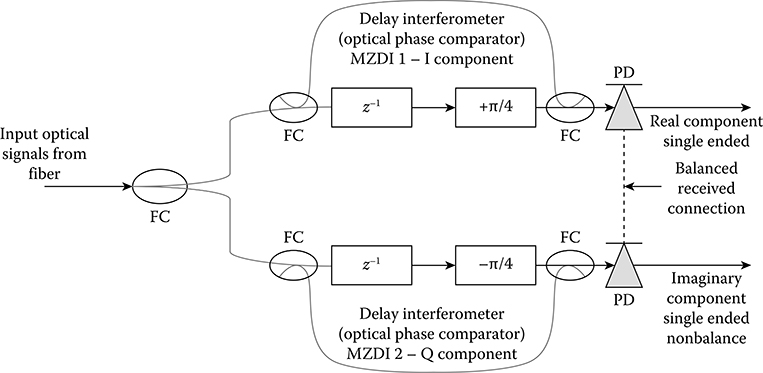
FIGURE 6.29 DQPSK receiver configuration using noncoherent direct detection. FC = fiber coupler, MZDI = Mach–Zehnder delay interferometer.
We now outline the purpose of the ±π/4 additional phase shift of the optical carrier implemented in the MZDI of the receiver. Because the two bits to be encoded at the Tx are implemented using an MZIM (0 or π phase shift) and the second bit is encoded via the PM (0 or π/2 phase shift), the two devices are said to be in quadrature to one another. This implies that there is a π/2 phase difference between all signaling phase states (Figure 6.26). The additional +π/4 and −π/4 give a total π/2 phase difference between the upper and lower receiver branches shown in Figure 6.22. Thus, recovery can be implemented by comparing the real and imaginary bits received to those transmitted. However, one can consider only the “real component” of the received signal and assess the overall performance of the system via eye diagram analysis (using the Q factor method and the BER). In practice, the demodulation of the DQPSK signal using the two-branch configuration in Figure 6.29 can be successfully demonstrated [9]. A balanced detection structure has been proven to be more sensitive (3 dB better) than the case of only a single photodetector. The eye diagram of the balanced detection of the transmission over noncompensated SSMF distance of 10 km and 5 km, are shown in Figure 6.30.
6.4.2 Offset DQPSK Modulation Format
In this section, we introduce offset DQPSK (O-DQPSK) transmission. ODQPSK has been applied in transmission over nonlinear satellite channels that offer a smoother transition between the phase states and hence avoids the π phase jumps as shown in Figure 6.31. In contrast to DQPSK, which requires detection at the symbol rate, the demodulation of ODQPSK can, however, be achieved at the bit rate, thus allowing the detection of the ODQPSK with only one set of balanced receivers and one set of MZDIs. Optical ODQPSK can be generated by two binary RZ-DPSK signals operated at half the bit rate that can be merged optically by a 3 dB coupler with a one-bit delay in one path as shown in Figure 6.32.
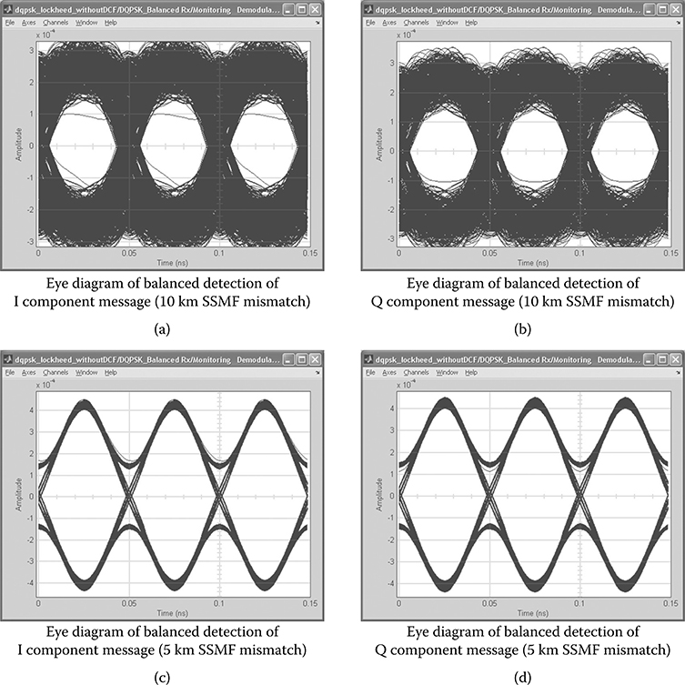
FIGURE 6.30 Eye diagrams achieved for I component: (a) 10 km SSMF, (b) 10 km SSMF, (c) 5 km SSMF; and for Q components (d) 5 km SSMF mismatch of dispersion over two 200 km dispersion compensated and optically amplified spans—RZ-DQPSK 50% RZ pulse shape.
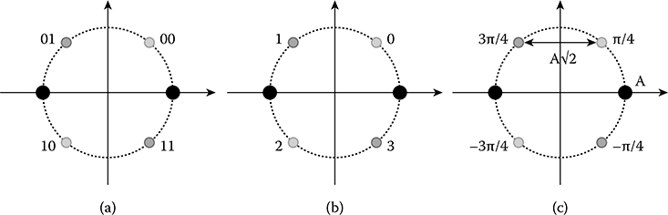
FIGURE 6.31 ODQPSK signal constellation and assignment of phase symbols: (a) quaternary digits, (b) two-digit binary word, and (c) phase complex plane with two state (horizontal line) circles are for DPSK constellation points.
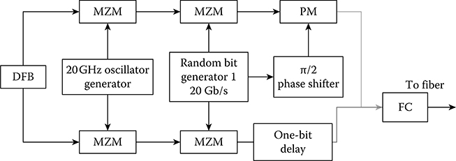
FIGURE 6.32 Schematic diagram of the optical offset DQPSK transmitter.
Similar to the case of DQPSK, a carrier phase difference of π/2 has to be guaranteed between two parallel signals to ensure the π/2 phase shift between the states of the constellation points similar to the phase plane shown in Figure 6.32. The receiver for the DQPSK modulation format can be implemented using only one MZDI and a balanced receiver, but only one MZDI is required and a π/2 phase shift must be inserted into one path of the MZDI to ensure the demodulation of the π/2 phase difference between consecutive bits, and hence the in-phase and quadrature components. If there is a cosine continuity of the phase shift between the constellation points, then the scheme ODQPSK becomes an MSK scheme, which was described in Chapter 5.
The receiver sensitivities of DQPSK, ODPSK, and DPSK have also been measured for a transmission over a 400 km span with optical amplifiers and DCF as shown in Figure 6.32. The bit rate for DPSK is 40 Gbps and 20 Gbps for DQPSK, and the input power to the fiber is set at 0 dBm to ensure that the systems operate under the linear regime. There are no differences between DQPSK and ODQPSK. A 6 dB difference between DQPSK and DPSK receiver sensitivities using a balanced receiver and a 3.5 dB difference between a single detector receiver and a balanced receiver for ODQPSK systems that is expected as the distance between the 1 and 0 is double that of a single detector as shown by the detected eye diagrams shown in Figure 6.16.
Two principal differences between the receiver sensitivities of RZ-DPSK and RZ-DQPSK are as follows: (1) Using the same total average power (i.e., the same radius on the phasor diagram; Figure 6.32), the binary level to the quaternary level would require an increase by a factor of 2 as we can observe from the signal constellations of DPSK and DQPSK. Thus, a 3 dB increase in the power is required for DPSK as compared with DQPSK. (2) For MZDI self-heterodyne detection, the detection seems to add an additional power penalty in the splitting and combining of the received optical fields. This is the complexity of the self-homodyne detection as compared to the coherent detection, in which the polarization can be diversified, while in the MZDI integrated lightwave circuitry, the polarization of the input lightwave coupled from the fiber would be reduced owing to the strong polarization dependence of the rib waveguide of the MZDI.
These original mechanisms of the reduction of the receiver sensitivity can be further explained as follows.
6.4.2.1 Influence of the Minimum Symbol Distance on Receiver Sensitivity
Assuming the noise pdf distribution at the receiver is Gaussian, coherent detection with matched filter would follow the well-known rule of the bit error probability, which depends on the Euclidean distance between the symbols and the variances at the levels of the symbols. In general, the noise power would have a mean of zero and a variance of σ2. With a minimum distance d between the symbols, the bit error probability Pe is given by
If the total average power of the signals is A2, then a binary DPSK has a Pe of
while the DQPSK would have a Pe of
The DQPSK allows the receiving of four bits in a symbol period while only two for the binary DPSK, thus the capacity of the DQPSK is double of that of the DPSK without increasing the noise contribution at the receiver output.
6.4.2.2 Influence of Self-Homodyne Detection on Receiver Sensitivity
The complexity of coherent detection with the use of a local laser and the synchronization of the phase of both the signals and the LO has been described in Chapter 3. With the advances in integrated lightwave technology, the MZDI can be implemented without difficulty and self-heterodyne detection can be assisted with the phase comparison; thus, self-heterodyne detection has attracted attention in current DPSK and DQPSK receivers or any receiver that would require the detection of the I and Q components using a balanced receiver. Under a matched filter condition of binary DPSK, the BER is approximately given by
For QPSK signals using an MZDI-balanced receiver for self-homodyne detection, the BER is given by Ref. [10]
where Q represents the Marcum function and I0 the modified Bessel function of the zeroth order, and A′ is the amplitude of the signal at the input of the PD. The BER versus the SNR can be estimated from Equations 6.18 through 6.21 which can also be modified for the case of coherent detection using balanced detectors [11]. However, a 2 dB improvement for DQPSK for the case of coherent over self-heterodyne detection is obtained. These results were obtained without considering the noise contribution in both the positive and negative electrical signal levels.
6.4.3 MATLAB® and Simulink® Model
6.4.3.1 Simulink® Model
MATLAB® and Simulink® models of the transmitter and receivers for the DQPSK modulation format are shown in Figures 6.33 and 6.34, respectively, with a π/4 phase offset of the signal constellation. A RZ-DQPSK optical transmission system is modeled with a pulse carver placed in cascade with the data optical modulator MZIM. A DQPSK precoder of two-bit per symbol provides the two output signals, the in-phase and the quadrature-phase components in the electrical domain which are amplified and used to drive the two arms of the optical MZIM. A π/2 PM is also used to assign the in-phase or quadrature-phase components of the DQPSK format.
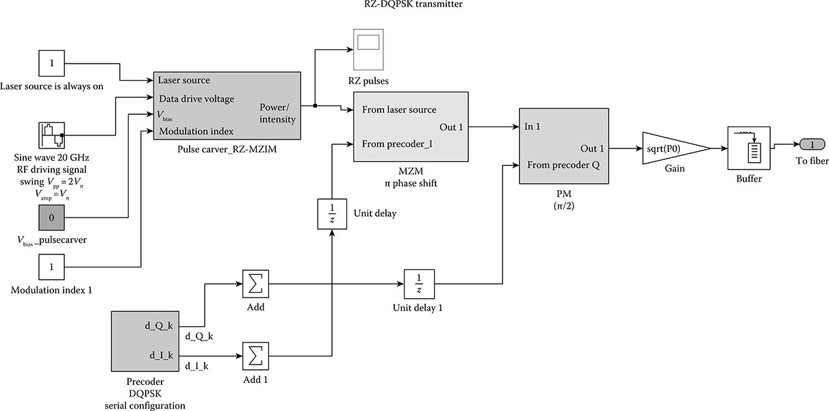
FIGURE 6.33 Transmitter MATLAB® and Simulink® model for DQPSK optical transmission.
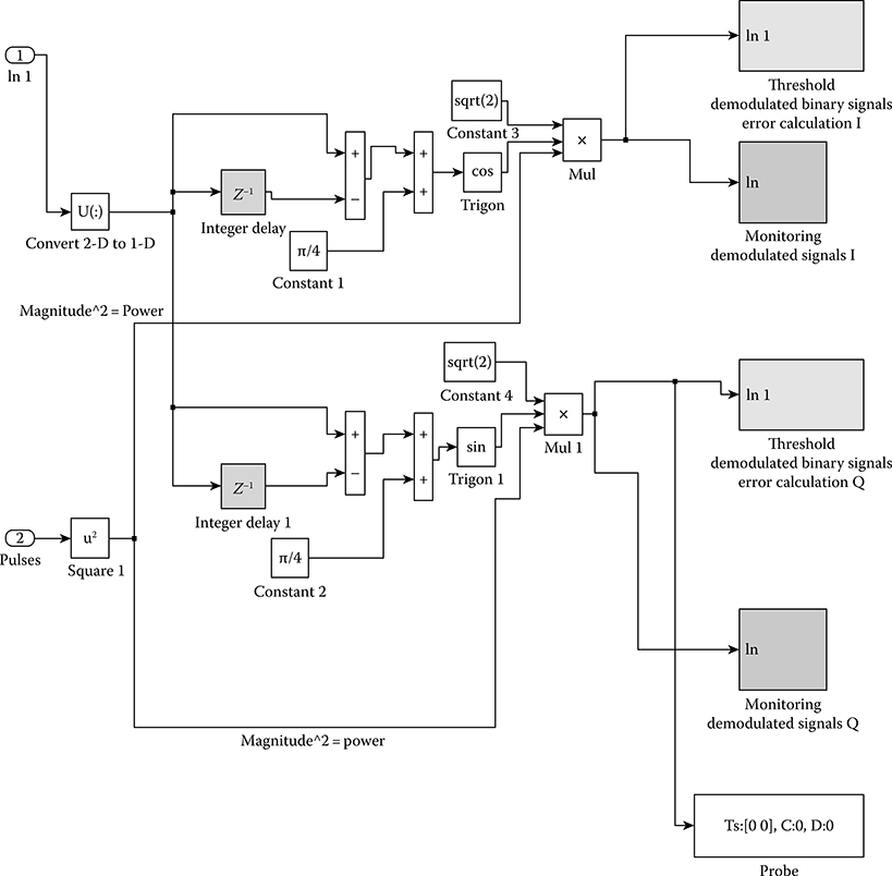
FIGURE 6.34 Receiver Simulink® model for DQPSK optical transmission.
In the receiver side, differential detection or self-homodyne receiving structures are used with a phase offset of π/4 to obtain directly the amplitude and phase of the receiving signals as discussed earlier.
6.4.3.2 Eye Diagrams
The transmission of the DQPSK with a bit rate of 40 Gbps or 20 Giga symbol/s conducted over SSMF lengths of 10 and 5 km are shown in Figure 6.35.
The length of SSMF is set to 10 km, and the length of DCF is set to be 2 km with the dispersion factor of the DCF set to be five times more negative than that of SSMF (full compensation) as shown in Figure 6.36.
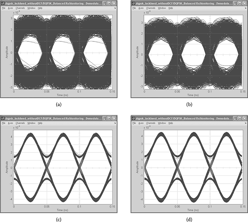
FIGURE 6.35 Eye diagram of DQPSK detected: (a) in-phase component, (b) quadrature component 10 km SSMF, and eye pattern of (c) the in-phase and (d) the quadrature components after 5 km SSMF transmission.

FIGURE 6.36 Arrangement of dispersion-compensated spans for transmission of DQPSK signals.
The Simulink models shown in Figures 6.37 and 6.38 illustrate how to set in the DCF block in the model. The length of DCF is set at 2 km and the dispersion factor to be five times more negative than that of SSMF for full dispersion compensation.
The measured eye diagrams of DQPSK are shown in Figure 6.39 at a total bit rate of 108 and 110 Gbps (or around 50 Gsymbol/s) when the I and Q components are detected separately and when both channels are turned on.
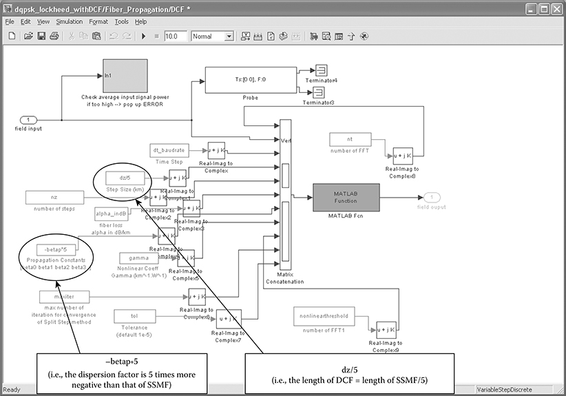
FIGURE 6.37 Simulink® model of the fiber sections of dispersion-compensating fiber (DCF) for fully compensated span.
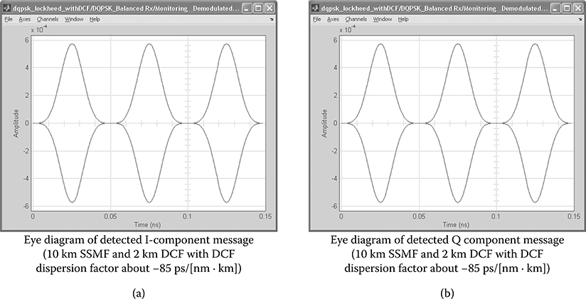
FIGURE 6.38 Simulated eye diagram of DQPSK detected: (a) in-phase component and (b) quadrature component, of a fully dispersion-compensated SSMF and DCF.

FIGURE 6.39 Measured eye diagrams of 108 Gbps RZ-DQPSK detected (50 Gsymbols/s): (a) in-phase component, (b) quadrature component, (c) both in phase and quadrature channels, (d) in-phase component, (e) quadrature component, and (f) both channels transmitted and one component is selected by tuning the MZDI. (Courtesy of SHF AG Berlin Germany).
6.5 Comparisons Of Different Formats and Ask and Dpsk
6.5.1 BER and Receiver Sensitivity
6.5.1.1 RZ-ASK and NRZ-ASK
It is obvious that if the pulse sequences of the NRZ and RZ (50% duty) ASK whose average powers are the same then because the FWHM of the RZ is half of that of NRZ, the peak amplitude of the RZ sequence would be higher than that of the NRZ. The higher the peak power of the RZ pulses, the greater the distance between the levels 0 and 1 and hence a possibility of an enhancement of the eye opening and thus BER.
Assuming now an equal average power of the two random NRZ and RZ data sequences, theoretically speaking, a higher peak power might not lead to better receiver sensitivity. However, according to the matched filtering concept [12,13], for any signal corrupted by additive white Gaussian noises in transmission systems with impulse responses of transmitter and receiver hT(t) and hR(t), the maximum SNR at the output of the matched filter is achieved and hR(t) = hT(t−T ) with T being the sampling delay time. Or alternatively, in the frequency domain, we have HR(f ). HT(f)exp(−j2πfT) = 1.
In the optical domain, such matched filters can be implemented using chirp fiber Bragg grating (FBG), thin-film filter, or microfilters for RZ pulses. Experimentally, it has been observed, as described earlier, that an improvement of about 2 dB can be achieved for the receiver sensitivity for RZ ASK as compared with NRZ-ASK, whereas the theoretical value is 3 dB.
6.5.1.2 RZ-DPSK and NRZ-DQPSK
Figure 6.40 shows the difference between the receiver sensitivity of the modulation formats RZ-DPSK and RZ-DQPSK under the detection structures of single and balanced detectors. A 3 dB improvement of the balanced receiver over that of the single detector is as expected from the push–pull mechanism of the balanced detection. This is known to be the maximum performance achievable with a balanced receiver with narrow band optical filtering at the input of the MZDI [14].
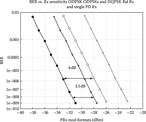
FIGURE 6.40 Optical DPSK and ODPSK transmission over 4 × 100 km SSMF of DWDM 8 × 40 Gbps transmission. Simulated results of BER versus receiver sensitivity of modulation formats: (o) Offset DQPSK– Balanced Rx, (left +) Offset DQPSK–single detector, (far right *) DQPSK–Balanced Rx, (far right +) DQPSK– single PD. * – offset DQPSK.
For RZ-DPSK and RZ-DQPSK under-balanced detection, there is a difference of 6–7 dB between these schemes. This is due to two possibilities: (1) Using the same averaged signal power, a factor is reduced between the distance of the 1 and 0 for DQPSK as is obvious from the signal constellations. (2) Using an MZDI at the input of the balanced detector pair, the optical power is split between the two MZDIs, so there is no gain in power, and even a loss occurred sometimes due to unused optical ports and scattering loss in the power split coupler.
6.5.1.3 RZ-ASK and NRZ-DQPSK
The comparison among ASK, DPSK, and DQPSK is important when differential phase with balanced receiving is used in the upgradation of 10 to 40 G rates as mentioned in Section 6.3.6. Theoretically and experimentally demonstrated as shown in Figure 6.22, the modulation format RZ-DPSK is expected to offer a 3 dB enhancement over the RZ-ASK and about 6 dB improvement as compared with NRZ-ASK. Thus, the performance of RZ-DQPSK would nearly be the same as RZ-ASK but with a symbol rate twice of that of NRZ or RZ-ASK. The Simulink and MATLAB model for RZ-DQPSK is given in the appendix at the end of this chapter.
This can be explained as follows: (1) The distance between the 1 and 0 of the ASK is nearly the same as that for DQPSK signals of the same average power as seen from the signal constellation shown in Figure 6.41; (2) the RZ format outperforms the NRZ format by 3 dB (maximum), and thus, RZ-DQPSK is expected to improve over NRZ-ASK by the same amount or less; and (3) the use of MZDI as an optical phase comparator at the input of the balanced detector pair would introduce an optical power loss owing to the splitting and unused ports, which can be improved using planar lightwave circuit (PLC) technology.
In summary, the use of multilevel modulation formats may result in optical loss and splitting when the MZDI-balanced receiving technique is used. These multilevel schemes would offer an effective high information capacity with the symbol rates much lower than that of the binary schemes, for example, 100 Gbps can be reduced to 25 Gsymbols/s if a two-level star-QAM is used. These multilevel modulation schemes will be described in Chapter 7.
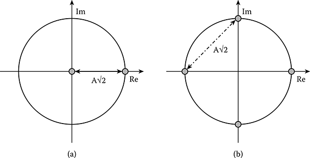
FIGURE 6.41 Signal constellation of (a) ASK and (b) DQPSK for the same average power.
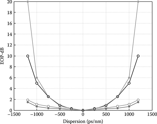
FIGURE 6.42 Measured and simulated dispersion tolerance of ASK and DQPSK (* gray – RZ-DQPSK, o dark gray RZ-ASK)—both RZ format of 50% duty cycle and NRZ-ASK (light gray *), NRZ-DPSK (light gray circle).
6.5.2 Dispersion Tolerance
Dispersion tolerance is the measure of the penalty of the eye opening at the receiver after the transmission whose dispersion over the number of spans is completely compensated with some extra residual dispersion. This is very important in practice because it would specify the maximum length of uncompensated fiber allowable during the installation of the transmission link.
Figure 6.42 shows the simulated and measured dispersion tolerances of 10 Gbps RZ-ASK and RZ-DPSK at 20 Gbps, which are effectively equivalent in the symbol rate. The tolerances of the modulation formats seem very close. This can be explained by observing the spectral distributions of these two modulation formats (Figure 6.14). The spectra of RZ-ASK and RZ-DPSK are very much the same except the peak power at the center of the passband of the RZ-ASK, which is understood as the contribution of the amplitude rising from 1 to 0 or vice versa. The 3 dB bandwidth is thus the same, and this contributes to the interference between the sidebands of the modulated lightwave. The RZ-DQPSK at 20 Gbps is equivalent to that of 10 Gbps DPSK, and thus we could state that the dispersion tolerance of the RZ-DQPSK would be equivalent to that of the 10 Gbps DPSK modulation format. A 1 dB penalty of the eye diagram or the eye opening penalty (EOP) is at a dispersion of 650 ps/nm for the two modulation formats, equivalent to 650/17 km of SSMF. The EOPs of the NRZ-ASK and NRZ-DPSK formats are also plotted against the dispersion to give a very similar pattern, as expected from their spectra. Note that for NRZ-DPSK, the data modulator is a dual modulator, and no chirp is introduced.
6.5.3 PMD Tolerance
Refs. [15, 16, 17, 18 and 19] have investigated the impact of PMD on DPSK, DQPSK direct detection formats. In systems with impairments dominated by first-order PMD, smaller duty cycle RZ formats would improve the resilience to the PMD by the ASK and DPSK systems as the ISI is smaller for narrower pulses. RZ-DQPSK is much more resilient to first-order PMD. DQPSK allows a DGD that is at least two times higher for the same EOP due to PMD as compared to that suffered by ASK and DPSK.
In systems in which the PMD is compensated, the second-order PMD would be minimized for modulation formats that offer narrower spectra because the second order is wavelength dependent, and hence a narrower spectrum would offer more resilience owing to second-order PMD effects.
6.5.4 Robustness Toward Nonlinear Effects
6.5.4.1 Robustness Toward SPM
The setup for investigation, both experimental and simulation, consists of four spans with 100 km SSMF and dispersion-compensating modules (DCMs) and associated EDF amplifiers at the end of SSMF and at the output of DCM with a booster EDFA and attenuator to adjust the input power launched to the transmission link. Four wavelength channels in the middle of the C-band are used. The EOP of a wavelength channel at 1552.95 nm is monitored and plotted against the launched power as shown in Figure 6.43 for the RZ-ASK and RZ-DQPSK modulation formats.
It is observed that the nonlinear SPM threshold for 1 dB EOP is 3 dBm, which is consistent with a 0.1π phase shift due to the nonlinear phase effect of a fiber with a nonlinear coefficient n2 = 2.3 × 10⁻²⁰ m−1. The nonlinear threshold for RZ-DQPSK is observed at around 7 dBm. By inspecting the spectra of ASK and DPSK, we note that because the amplitude is switched on and off, there is transitional time, or, equivalently, the sampling time of the sequence and the Fourier transform of the sequence would have spikes at the sampling frequency. This peak power level and hence the average power of the ASK sequence is contained mostly in the carrier peaks. Unlike in DPSK or DQPSK, the envelope is constant and the energy is contained mostly in the signal as we could observe no peaks in their spectra. Thus, RZ-DQPSK and RZ-DPSK data sequence would be more tolerant to the SPM effects.
6.5.4.2 Robustness toward Cross-phase Modulation
In 40 Gbps systems, the nonlinear SPM effects dominate the impairments due to fiber nonlinearity. However, in 10 Gbps DWDM systems, the situation is different, especially for 100 GHz spacing [20]. The cross-phase modulation (XPM) is caused by the nonlinear phase effects of a channel in the DWDM system, especially when its intensity is fluctuating, which would cause a phase disturbance in other channels. This PM disturbance would then be transferred to other channels with amplitude modulation. The XPM effects can be considered to contribute to the frequency spectrum via a transfer function [21] given by
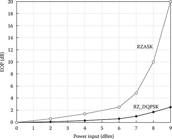
FIGURE 6.43 EOP induced by SPM versus input power at the beginning of the fiber transmission links of 4 × 100 km fully compensated SSMF spans at a bit rate of 40 Gbps. RZ-ASK (circle) RZ-DQPSK (star).
where γ1 is the nonlinear factor due to the intensity fluctuation of wavelength λ1 channel, α is the attenuation factor, and d12 (d12z = D(λ1−λ2)z) is the group delay difference between the two channels λ1 and λ2 over a distance z. Thus, for 100 GHz spacing and over SSMF of D = 17 ps/nm/km, the 3 dB passband of this low-pass filter transfer function is at about 540 MHz, which would fall into the signal bands of a 10 Gbps bit rate system.
Shown in Figure 6.44 is the EOP due to an XPM of 10 Gbps 100 GHz spacing DWDM transmission of RZ-ASK and RZ-DPSK over multispans link in which both dispersion and attenuation effects are equalized with DCM and EDFAs. Clearly, the DPSK format is much more tolerable to the XPM effects as compared to that of RZ-ASK. The XPM effect could be reduced by using an electrical filter of a corner frequency about the 540 MHz with a sharp roll-off factor placed at the output of the electronic preamplifier.
6.5.4.3 Robustness toward four-wave mixing
Unlike the impairments due to SPM and XPM mainly caused by the optical power of the channels, four-wave mixing (FWM) effects come from the relative phase difference between the channels. We can summarize the influence of FWM on DPSK and DQPSK signals as follows.
For dispersion-shifted fibers, the phase velocity of different channels around the zero-dispersion wavelength region is the same, and thus phase matching would occur and enhance the generation of the fourth wave that would fall within the active band of an equally spaced DWDM system. Figure 6.45a and b shows simulated results of the EOP of the fourth channel versus the peak and average power of three NRZ-ASK and NRZ-DPSK channels with 100 GHz spacing in the region of zero-dispersion wavelength of DSF.
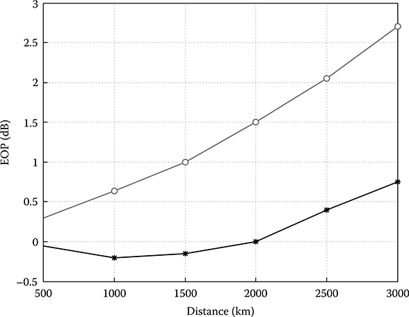
FIGURE 6.44 EOP induced by XPM versus total transmission distance (dispersion-compensated and attenuation-equalized spans).
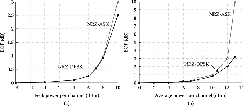
FIGURE 6.45 EOP induced by FWM versus (a) launched power (peak) and (b) average power of three NRZ-ASK and NRZ-DPSK channels after 100 km DSF with zero-dispersion wavelength at 1552.93 nm.
6.5.4.4 Robustness toward Stimulated Raman Scattering
The impact of stimulated Raman scattering (SRS) on different modulation formats has been reported [22], including the formats DPSK and DQPSK, which have been shown to improve significantly the resilience to SRS crosstalk, especially when the RZ formats are employed, the SRS effects are negligible. The principal reasons are the periodic variation of the optical power or field propagating through the fiber, and the consequent absence of low-frequency components to enhance the SRS effects. The effect is very much like that of XPM but at a lower frequency. Thus, RZ-DPSK would not exhibit low frequency due to SRS. Simulated results of the effects of SRS on the broadening of NRZ pulse ASK modulation over the number of spans of SSMF and NZ-DSF, completely optically amplified and dispersion compensated, are shown in Figure 6.46. The SRS effects on the pulse broadening of RZ-DPSK are also shown to be significantly undisturbed by the periodic variation of the phase of the carrier, which explains the strong resilience of the modulation format to SRS. The standard deviation of the pulse amplitude over the average signal level is measured as a percentage.
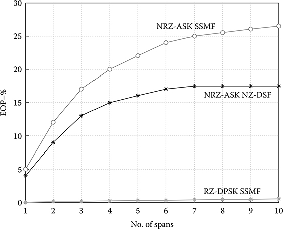
FIGURE 6.46 Percentage broadening of the 1 level (% of pulse period) due to SRS crosstalk for 11 channels with 4 nm spacing and 10 Gbps bit rate under SSMF and NZ-DSF fiber spans. Modulation format NRZ-ASK. Span length = 100 km SSMF fully dispersion compensated.
6.5.4.5 Robustness toward Stimulated Brillouin Scattering
All DPSK and DQPSK do not exhibit the carrier component at the center of the passband of the spectrum, and thus it can be stated that stimulated Brillouin scattering would play no role in phase shift keying modulation formats.
6.6 Concluding Remarks
This chapter gives the fundamental aspects of the optical transmission of discrete phase modulation formats (DPSK, DQPSK, and ASK) as well as the structures of the transmitters and receivers. Experimental setups for the transmission of modulation formatted signals, NRZ, RZ, CSRZ, NRZ-DPSK, RZ-DPSK, CSRZ DPSK, and so on over optically amplified dispersion-compensating systems have been described. Experiments have investigated the filtering effects on performance of the transmission systems, the dispersion tolerance, and receiver sensitivity performance of RZ-ASK and RZ/CSRZ-DPSK. The filtering properties of the muxes and demuxes do not significantly affect the transmission performance in terms of the BER and receiver sensitivity of the 40 Gbps RZ or CSRZ-DPSK modulation formats.
FIGURE 6.47 Siemens TranXpress multiwavelength transport systems.
We have also reported and simulated the nonlinear effects, including SRS, SPM, XPM, and SBS, on the eye opening at the receiver of phase shift keying modulation, in particular, DPSK and DQPSK with RZ formats. Phase shift keying modulation is much more resilient to the nonlinear effects as compared to ASK.
The negligible mutual effects of adjacent 40 Gbps DPSK channels on 10 Gbps ASK-modulated transmission channels enable the feasibility of the upgradeability of the 10 Gbps current system to 40 Gbps optical DPSK-modulated transmission. We have also measured the transmission quality of both 40 and 10 Gbps channels and observed no significant degradation of either channel by the other. Our next step is to launch the 40 Gbps modulation format over a commercial system, the Siemens multiwavelength transport TranXpress system, as shown in Figure 6.47, and then over an installed multiwavelength 10 Gbps transmission link between cities, for example, Melbourne and Sydney of Australia.
Appendix 6A: Matlab® and Simulink® Model For Dqpsk Optical System
A number of models in MATLAB and Simulink are given in Figures 6A.1 through 6A.4. Figure 6A.1 gives the block diagram of the entire transmission system, generally an optical transmitter, the optically amplified fiber spans, and then the receiver, including subsystems for evaluation of the BER versus parameters such as receiver sensitivity, EOP, and so on. Figure 6A.2 gives the model of optical transmitters together with Figure 6A.3 as a precoder in the electrical domain to generate signals for driving the electrodes of the MZIM. Figure 6A.4 gives the model of a balanced receiver incorporating the MZDI as a phase comparator for DPSK.
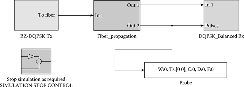
FIGURE 6A.1 General schematic diagram of the DQPSK system.
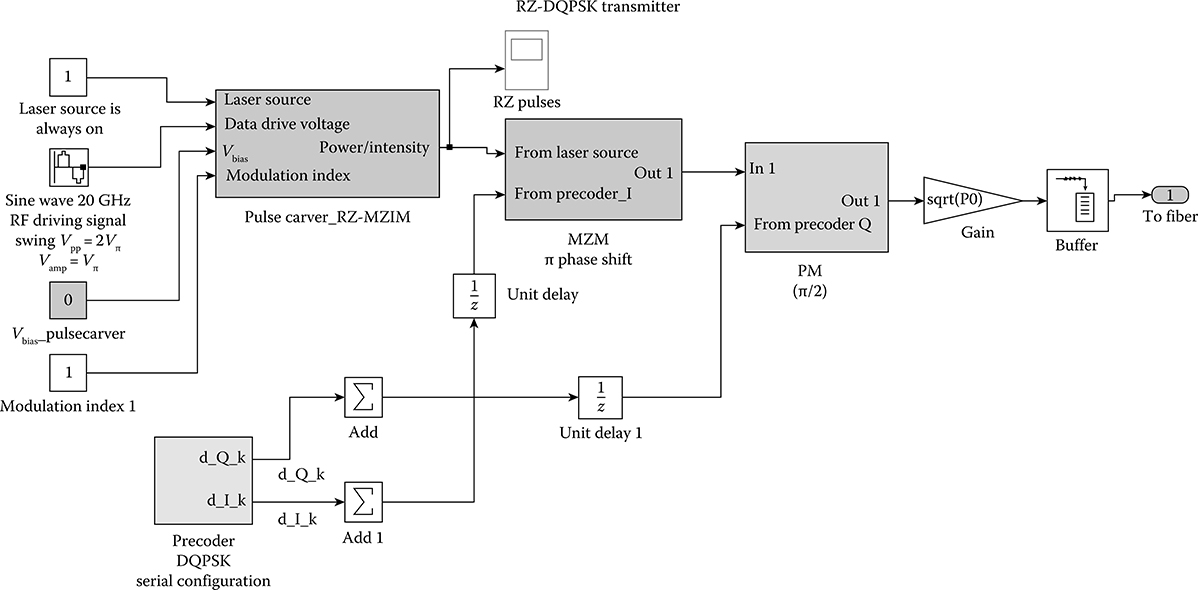
FIGURE 6A.2 Simulink® model of the optical transmitter for RZ-DQPSK.
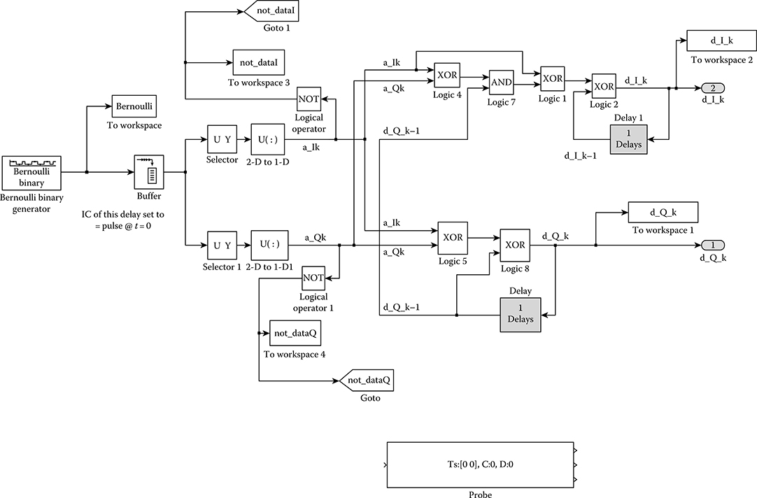
FIGURE 6A.3 Simulink® model of the electrical precoder for optical transmitter for RZ-DQPSK.
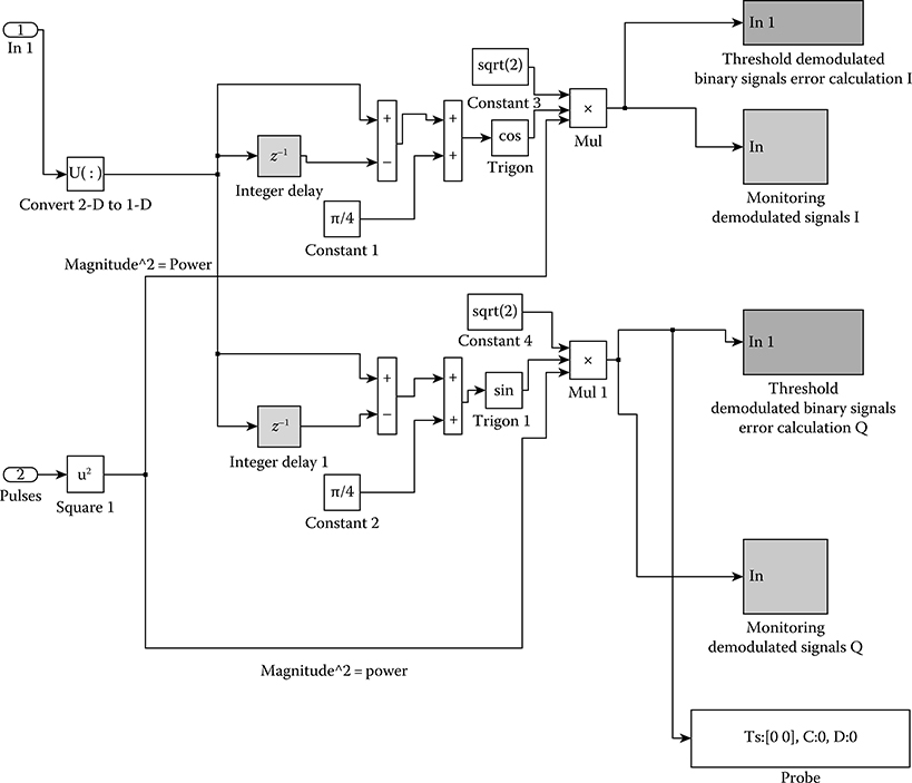
FIGURE 6A.4 Simulink® model of the MZDI optical balanced receiver for RZ-DQPSK.
References
1. P. J. Winzer, Optical transmitters, receivers, and noise, in Wiley Encyclopedia of Telecommunications, J. G. Proakis, Ed., New York: Wiley, 2002, pp. 1824–1840.
2. P. J. Winzer and R.J. Essiambre, Advanced optical modulation formats, in Proceedings of the ECOC 2003, Rimini, Italy, 2003, invited paper Th2.6.1, pp. 1002–1003.
3. L. N. Binh, Lithium niobate optical modulators, in International Conference on Material and Technology Symposium M: Material and Devices, Singapore, July 2005.
4. R. A. Linke and A. H. Gnauck, High-capacity coherent lightwave systems, J. Lightwave Technol., Vol. 6, No. 11, pp. 1750–1769, 1988.
5. J.X. Cai, D. G. Foursa, C. R. Davidson, Y. Cai, G. Domagala, H. Li, L. Liu, et al., A DWDM demonstration of 3.73 Tb/s over 11 000 km using 373 RZ-DPSK channels at 10 Gb/s, in Proceedings of the OFC 2003, postdeadline paper PD22, Atlanta, GA, 2003.
6. J. C. Livas, E. A. Swanson, S. R. Chinn, E. S. Kintzer, R. S. Bondurant, and D. J. DiGiovanni, A one-watt, 10-Gbps high-sensitivity optical communication system, IEEE Photon. Technol. Lett., Vol. 7, pp. 579–581, 1995.
7. A. H. Gnauck, X. Liu, X. Wei, D. M. Gill, and E. C. Burrows, Comparison of modulation formats for 42.7-Gb/s single-channel transmission through 1980 km of SSMF, IEEE Photon. Technol. Lett., Vol. 16, pp. 909–911, 2004.
8. C. Wree, RZ-DQPSK Format with High Spectral Efficiency and High Robustness towards Fiber Nonlinearities, Technical report, University of Kiel, Kiel, Germany.
9. C. Wree, Experimental investigation of receiver sensitivity of RZ-DQPSK modulation format using balanced detection, in Proceedings of the OFC2003, paper ThE5, Vol. 2, p. 456, 2003.
10. Y. Okunev, Phase and Phase Difference in Digital Communications, Artec House, Boston, 1997.
11. C. Wree, Differential Phase Shift Keying for Long Haul Fiber-Optic Transmission Based on Direct Detection, Dr. Ing. Dissertation, CAU University zu Kiel, Kiel, Germany, p. 75, 2004.
12. S. Benedetto and E. Biglieri, Principles of Digital Communications with Wireless Applications, New York: Kluwer Academics, 1999.
13. K. K. Pang, Digital Communications, Lecture notes, Monash University, Melbourne, Australia, 2002.
14. A. H. Gnauck and P. J. Winzer, Optical phase-shift-keyed transmission, IEEE J. Lightwave Technol., Vol. 23, No. 1, pp. 115–130, 2005.
15. C. Xie, L. Moeller, H. Haustein, and S. Hunsche, Comparison of system tolerance to polarization mode dispersion between different modulation formats, IEEE Photon. Technol. Lett., Vol. 15, No. 8, pp. 1168–1170, 2003.
16. J. Wang and J. M. Kahn, Impact of chromatic and polarization mode dispersion on DPSK systems using interferometric demodulation and direct detection, IEEE J. Lightwave Technol., Vol. 10, pp. 96–100, 2004.
17. H. Kim, C. R. Doerr, R. Pafchek, L. W. Stulz, and P. Bernasconi, Polarization-mode dispersion impairments in direct-detection differential phase-shift-keying systems, Electron. Lett., Vol. 38, No. 18, pp. 1047–1048, 2002.
18. R. A. Griffin, R. I. Johnstone, R. G. Walker, J. Hall, S. D. Wadsworth, K. Berry, A. C. Carter, et al., 10 Gb/s optical differential quadrature phase shift key (DQPSK) transmission using GaAs/AlGaAs integration, in Proceedings of the OFC 2002, postdeadline paper FD6, Anaheim, CA, 2002.
19. R. A. Griffin and A. C. Carter, Optical differential quadrature phase shift keying (oDPSK) for high capacity optical transmission, in Proceedings of the Optical Fiber Communications Conference OFC 2002, paper WX-6, 2002.
20. P. Mitra and J. Stark, Nonlinear limits to the information capacity of optical fiber communications, Nature, Vol. 411, pp. 1027–1070, 2001.
21. C. Wree, Differential Phase Shift Keying for Long Haul Transmission Based on Direct Detection, Dr. Ing Dissertation, CAU University zu Kiel, Kiel, Germany, pp. 24, 2002.
22. S. Schoemann, J. Leibrich, C. Wree, and W. Rosenkranz, Impact of SRS-induced crosstalk for different modulation formats, in Proceedings of the Optical Fiber Conference., OFC 2004, paper FA5, 2004.