
7
Multilevel Amplitude and Phase Shift Keying Optical Transmission
This chapter presents the modulation formats that combine the amplitude modulation and differential phase modulation schemes and the multilevel amplitude and phase shift keying (PSK). Comparisons between multilevel and binary modulation are made. Critical issues for transmission performance for multilevel modulation are identified. A simulation platform based on MATLAB® and Simulink® is described. Furthermore, for reaching 100 Gbps Ethernet, a number of multilevel modulations such as PSK and orthogonal frequency division multiplexing (OFDM) are proposed and described in the last section of the chapter.
7.1 Introduction
Under the conventional on-off keying (ASK) modulation format, the transmission bit rate beyond 40 Gbps per optical channel is very costly because the electronic signal processing technology may have reached its fundamental speed limit. It is expected that advanced photonic modulation formats such as M-ary amplitude and differential phase shift keying would replace ASK in the near future. These advanced formats would offer efficient spectral properties, thus making it possible to increase the transmission rate without placing stringent requirements on high-speed electronics and to use the same existing photonic communication infrastructure.
Coherent communications developed in the mid-1980s and has extensively exploited different modulation techniques to improve the optical signal-to-noise ratio (OSNR) [1]. However, coherence detection has faced considerable difficulties owing to the stability of the source spectrum and the laser linewidth for gain in the receiver sensitivity of a mere 3 dB for heterodyne detection and 6 dB for homodyne detection in order to extend the repeaterless distance of 60–80 km of standard single-mode fiber (SSMF).
The invention of the optical amplifier (OA) in the early 1990s has overcome the fiber attenuation limit and thus offers a significant improvement in optical transmission technology. Because of this, ultra-long-haul and ultra-high-capacity optical transmission systems have been deployed widely around the world in the last decade. The technology has matured with ASK modulation reaching 10 Gbps per optical channel, a total channel count of hundreds, and with 100/50 GHz channel spacing [2].
Based on proven efficient spectra and transmission technology, especially the controllable total dispersion of the transmission and compensating fibers, it is much more advantageous that these spectral regions be efficiently used. Therefore, the contribution of advanced modulation techniques and formats would offer higher spectral efficiency for photonic transmission.
Further, digital modulation techniques have been well established over the last half century with amplitude, frequency, or phase modulations [3]. These techniques, especially phase modulation, rely principally on the detection schemes, that is, on whether it is coherent or pseudo-coherence differential detection, and have been heavily exploited in wireless communication networks. In the photonic domain, for a long time the technological difficulties associated with manufacturing narrow-linewidth lasers have prevented the use of coherent and differential phase modulation. Only over the last several years, due to the maturity of the laser technology, particularly the successful development of distributed feedback (DFB) laser, has the laser linewidth reached a level that is much smaller than the modulation bandwidth. The coherence of the sources is now sufficient for differential phase modulating and detecting applications that require the phase of the sources to remain stable over at least two consecutive symbol periods [4].
Recently, advanced modulation techniques have attracted significant interest from the photonic transmission research and systems engineering community. Several modulation schemes and formats such as binary differential phase shift keying (BDPSK), differential quadrature phase shift keying (DQPSK), duobinary ASK associated with non-return-to-zero (NRZ), return-to-zero (RZ), and carrier-suppress return-to-zero (CSRZ) formats have been widely studied [5, 6, 7 and 8]. However, what have not been widely explored are optical multilevel modulation schemes. Although multilevel schemes have been intensively exploited in wireless communications [6,9,10], there are only a small number of studies to date that incorporate the in-coherent multilevel optical amplitude phase shift keying modulation schemes that offer the following advantages:
Lower symbol rate; hence for the same available spectral region, a multilevel modulation scheme would offer a transmission capacity higher than its binary modulation counterparts.
Efficient bandwidth utilization; photonic transmission of these multilevel signals could be implemented over the existing optical fiber communications infrastructure without significant alteration of the system architecture, thus saving the cost of capital investment and easing the system management.
The complexity of the coder and demodulation subsystems falls within the technological capabilities of current microwave and photonic technologies.
The principal objectives of this chapter are
To evaluate different modulation and coding techniques and signal pulse formats for long-haul ultra-high-capacity transmission and thus determine novel modulation schemes, such as multilevel amplitude phase shift keying, and others to be determined, for research studies.
To develop analytical, simulation, and experimental test beds to demonstrate the uniqueness and superiority of our novel schemes.
A comparative study of the modulation formats so as to unveil the principal directions for photonic modulation and transmission technologies for the next transmission generation.
A novel photonic communication system based on advanced multilevel optical modulation formats and implementation of the system on the Simulink platform to demonstrate its effectiveness and superiority to its counterparts and to demonstrate its feasibility as a useful platform for desktop computer simulation.
Thus, a conceptual photonic transmission system is proposed based on a hybrid technique that combines phase and amplitude modulation, the multilevel amplitude differential phase shift keying (MADPSK) format. This technique combines two modulation formats: the well-known M-ary ASK and the M-ary DPSK to take advantage of high receiver sensitivity and dispersion tolerance (DPSK), and the enhancement of total transmission capacity (M-ASK) as compared to the traditional ASK format.
The models of the MADPSK transmitter and receiver have been structured for MADPSK signaling. A simulation model based on the MATLAB and Simulink platform has been developed for the proof of concept. The system performance is evaluated for back-to-back and long-haul transmission. The analytical and simulation results of the transmission configurations are demonstrated. The following are presented:
Noise mechanisms, for example, quantum shot noise, quantum phase noise, optically amplified noise, noise statistics, nonlinear phase noise; hence, the design of an optimum detection and decision-level schemes for MADPSK
Linear and nonlinear and polarization dispersion impairments and their impact on MADPSK system performance
Matched filter design for optimum MADPSK signal detection
Offset MADPSK (O-MADPSK) modulation schemes
MAMSK modulation
MADPSK modulation for applications in subcarrier transmission systems, especially for metropolitan wide area multi-add/drop networks
Other issues or additional modulation formats suitable for MADPSK
This chapter is thus organized as follows: Section 7.1 gives a brief review of a number of advanced photonic modulation formats. Section 7.2 reviews and compares different modulator structures used for generating advanced photonic modulation signals and emphasizes the advantages of a dual-drive Mach–Zehnder intensity modulator (MZIM) as a modulator for generating an MADPSK signal, the main objective of the study. Section 7.3 identifies a number of critical issues and alternative multilevel signaling for optical systems. In Section 7.4, a novel photonic transmission system with the MADPSK modulation format is proposed. Section 7.5 summarizes the preliminary studies and results.
7.2 Amplitude And Differential Phase Modulation
7.2.1 ASK Modulation
7.2.1.1 NRZ-ASK Modulation
ASK has been the dominant modulation technique from the early days of optical communications. The main advantage of this modulation is that the ASK signal is not sensitive to the phase noise. ASK modulation can take two principal formats: the first one is called NRZ-ASK, in which the one optical bit occupies the entire bit period; in the second one, RZ-ASK, the one bit is present in only the first half of the bit period.
Figure 7.1 shows the spectrum of a 40 Gbps NRZ-ASK signal, with the carrier seen at the highest peak and the 3 dB bandwidth reaching the bit rate. The main advantage of the NRZ-ASK signal is that its spectrum is generally the most compact compared with that of other formats such as RZ-ASK and CSRZ-ASK. On the contrary, the NRZ-ASK signal is affected by fiber chromatic dispersion (CD) and is more sensitive to fiber nonlinear effects as compared to its RZ- and CSRZ-ASK counterparts.

FIGURE 7.1 Spectrum of 40 Gbps NRZ-ASK signal.
7.2.1.2 RZ-ASK Modulation
The RZ-ASK signal, shown in Figure 7.2 [7], is similar to the NRZ-ASK signal, except that the one bit occupies only the first half of the bit period. This signal can be generated by a transmitter shown in the same figure in which an NRZ-ASK transmitter is followed by a pulse carver driven by a pulse train synchronized with the data source. The pulse train has a frequency equal to the data rate. The RZ-ASK pulse width can take the form of 33%, 50%, and 66% duty ratio. Because of its narrower pulse width, the spectrum of the RZ-ASK signal, shown in Figure 7.3, is larger than that of the NRZ-ASK signal, which decreases the spectrum efficiency. In this spectrum, the carrier is seen as the highest peak, and the two side peaks are RF modulating signals positioned 80 GHz apart.
7.2.1.3 CSRZ-ASK Modulation
The CSRZ-ASK modulation format [11] is similar to the standard RZ-ASK format, except that the neighboring optical pulses have a π phase difference. The carrier in neighboring time slots is thus cancelled out and effectively excluded from the signal spectrum. The CSRZ-ASK signal can be generated by a transmitter with the scheme shown in Figure 7.4 [11]. In this scheme, the first MZIM modulates the intensity of the optical signal coming from a laser source, while the second MZIM, driven by a clock signal whose rate is equal to half of that of the data rate, caves the NRZ pulses into RZ ones. Because the second MZIM is biased at the minimum-intensity point, it provides an RZ pulse train at the data rate with alternating phases 0 and π for neighboring time slots. The CSRZ-ASK signal can also be detected by a direct detection receiver as it would not be phase sensitive.

FIGURE 7.2 RZ-ASK transmitter and signal. (Adapted from T. Mizuochi et al., IEEE J. Lightwave Technol., Vol. 21, No. 9, pp. 1933–1943, 2003.)

FIGURE 7.3 Spectrum of 40 Gbps 50% RZ-ASK signal.

FIGURE 7.4 (a) Block diagrams of CSRZ-ASK transmitter and (b) generation of optical pulse with alternative phase using biasing control and amplitude. (Adapted from Y. Miyamoto et al., IEEE Electron. Lett., Vol. 35, No. 23, pp. 2041–2042, 1999.)
The main advantages of CSRZ-ASK include a narrower spectrum, higher tolerance to dispersion, and stronger robustness against fiber nonlinear effects as compared with standard RZ-ASK. Because its peak optical power is much lower than that of other formats, it is less affected by both self-phase modulation (SPM) and cross-phase modulation (XPM) [7]. Figure 7.5 shows the spectrum of 40 Gbps CSRZ-ASK signal with a very low carrier power level [12].
ASK is a modulation technique that generates a signal s(t) by multiplying a digital signal m(t) by a carrier fc [13]
where A is the amplitude envelope; the digital signal m(t) may take one of M levels [b0, b1,...,bM. When M = 2, s(t) is a binary ASK signal with ASK as a special case. ASK is also implemented in NRZ, RZ, and CSRZ formats, whose spectra are shown in Figure 7.6 in the same graph for the purpose of comparison. Like their ASK analogs, NRZ-ASK has the most compact spectrum, whereas RZ-ASK has the broadest. In terms of energy, CSRZ-ASK has the lowest peak power because the carrier signal has been effectively removed.

FIGURE 7.5 Spectrum of 40 Gbps CSRZ-ASK. (Extracted from L. N. Binh et al., DPSK RZ modulation formats generated from dual-drive interferometric optical modulators. Unpublished works.)

FIGURE 7.6 Spectrum of NRZ-ASK, RZ-ASK, and CSRZ-ASK signals.
7.2.2 Differential Phase Modulation
Under ASK/ASK modulation schemes with the associated NRZ, RZ, and CSRZ formats, the amplitude of the optical carrier varies accordingly. Phase modulation, on the contrary, modulates the carrier phase and thus facilitates the use of bipolar signals “±1.” This distinguishing feature means that phase modulation offers a significant improvement in receiver sensitivity as compared with ASK modulation. With the recent advances in photonic lightwave technology, especially the integrated optic delay interferometer, differential phase modulation and demodulation and the balanced receiver have become realizable. This section gives a brief overview of the differential modulation techniques and their implementations in the photonic domain, especially the MADPSK.
The term NRZ-BPSK, or traditionally NRZ-DPSK, is commonly used for denoting a modulation technique in which the optical carrier is always present with a constant power, with its phase alternating between 0 and π. The modulation rule is as follows
At the transmitter: Initially a reference 0 bit is entered as the present encoded bit. Then the next data bit is compared with the present encoded bit. If they are different, then the next encoded bit is 1, for which a phase change of π occurs, else the next encoded bit is 0, which causes no (or 0) phase change.
At the receiver, the phase of the carrier at the present bit slot is compared with that of the previous one. If the phase difference is π, then the data is decoded as 1, otherwise the data is 0 when the phase difference is 0.
One of the NRZ-DPSK transmitter structures is shown in Figure 7.7 [14]. User data are first encoded by a differential encoder into the driving voltage which then alternates the phase of the carrier signal between 0 and π. In detecting a NRZ-DPSK signal, a delay Mach–Zehnder interferometer (MZI) in combination with a balanced optoelectronic receiver can be used. The interferometer acts as the phase comparator with constructively and destructively interfered outputs.
As shown in Figure 7.7, the received optical signal is split into two arms of an MZI, one of which has a one-bit optical delay. The MZI compares the phase of each bit with the phase of the previous bit, and the photodetector converts the phase difference to the intensity. When there is no phase shift between two bits, they are added constructively hence giving maximum resultant amplitude to the output signal; otherwise, they cancel out when the phase shift equals π. If the differential phase shift is Δ ϕ, then the differential current at the output of the balanced photodetector can be written as
Because the balance receiver uses both the constructive and destructive ports of the MZI, the detected signal level can swing from 1 to −1. Compared with ASK or with the use of the unbalanced receiver where the signal amplitude is limited between 1 and 0, DPSK can offer a 3 dB improvement in receiver sensitivity.
Due to its constant envelope, the NRZ-DPSK signal is less sensitive to power modulation-related nonlinear effects, such as SPM and XPM, than its NRZ-ASK counterpart [15,16]. On the contrary, long-haul DPSK systems, including both NRZ and RZ, with OA are affected by nonlinear phase noise. The amplified spontaneous emission (ASE) noise of OAs is converted into phase noise, leading to waveform distortion and, consequently, signal degradation. The spectrum of the NRZ-DPSK signal is shown in Figure 7.8 [17], together with other DPSK formats. It can be seen that the NRZ-DPSK signal has the most compact spectrum compared with that of other DPSK formats.

FIGURE 7.7 (a) NRZ-DPSK signal, (b) transmitter, and (c) receiver. (Adapted from R. Hui et al., Advanced optical modulation formats and their comparison in fiber-optic systems, Technical Report, Information and Telecommunication Technology Center, University of Kansas, 2004.)
This can be explained by the fact that the NRZ-DPSK signal amplitude remains constant regardless whether bit 1 or bit 0 is transmitted, and thus the energy is distributed more equally compared to RZ- and CSRZ-DPSK signals.
The RZ-DPSK format is similar to the NRZ-DPSK format, the only difference being that instead of constant optical power, a pulse narrower than the bit period appears in each bit slot as shown in Figure 7.9. The RZ-DPSK transmitter, however, resembles an RZ-ASK transmitter in which the phase modulator (PM) replaces the intensity modulator (IM). The RZ-DPSK signal can also be detected by the same receiver used for the NRZ-DPSK signal. Owing to its narrow pulse, the RZ-DPSK format is expected to minimize the effects of intersymbol interference and is thus capable of achieving a longer transmission distance [7]. A narrow pulse, however, spreads the spectrum of the RZ-DPSK signal wider than that of the NRZ-DPSK signal, making RZ-DPSK systems more susceptible to CD. To reduce the effect of this impairment, CD compensation devices are used.

FIGURE 7.8 Experimentally measured spectra of NRZ-DPSK, RZ-DPSK, and CSRZ-DPSK signals. (Extracted from T. L. Huynh et al., Long-haul ASK and DPSK optical fiber transmission systems: Simulink modeling and experimental demonstration test beds, Proc. IEEE Tencon’05, Melbourne, Australia, November 2005.)
RZ-DPSK signal energy is not distributed equally as in the case of NRZ-DPSK. Most of it is concentrated in only a fraction of the bit duration, while it reduces to nearly zero for the rest of the time. This large energy fluctuation makes the signal more susceptible to fiber nonlinearity and makes signal detection more difficult.
The carrier suppression technique can also be used in conjunction with RZ-DPSK modulation to produce a CSRZ-DPSK signal, which has been demonstrated as one of the most attractive modulation formats in high-spectral-efficiency wavelength division multiplexing (WDM) and dense WDM (DWDM) systems [15].
It is due to the suppression of the carrier, the CSRZ-DPSK modulation format offers higher energy and spectral efficiency, and hence more resilience to impairments due to the fiber nonlinearity, CD and polarization-mode dispersion (PMD) as compared its RZ-DPSK counterpart. The spectra of CSRZ-DPSK, RZ-DPSK, and NRZ-DPSK are shown together in Figure 7.8 for comparison.
The CSRZ-DPSK signal can be generated by a transmitter whose scheme, shown in Figure 7.10, for the ASK parts is similar to that of CSRZ-ASK. The main difference is that in the CSRZ-DPSK transmitter a PM replaces the IM used in the CSRZ-ASK transmitter. The receiver for CSRZ-DPSK has the same structure as that of the NRZ-DPSK scheme.
To increase transmission bit rate without an increased bandwidth requirement, one can code more than one bit into a data symbol. DQPSK modulation is the first step in the realization of this idea [18, 19 and 20].
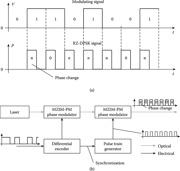
FIGURE 7.9 (a) RZ-DPSK signal and (b) and transmitter structure.
A signal constellation or signal space is the best way to represent a DQPSK signal, in which the points representing phase-modulated signals are located on two orthogonal axes called I and Q (for in-phase and quadrature components, respectively). Each of the two data bits [D1,D0] is first precoded into a symbol, and then the symbol is encoded into a phase shift that may take one of four values [0, π/2, π, 3π/2] depending on the bit combination it represents. The DQPSK symbol rate is thus equal to only half the bit rate. The constellation of QPSK is shown in Figure 7.11. Intuitively, one can say that with the same bandwidth available, DQPSK offers twice the transmission capacity compared with its ASK and binary DPSK counterparts.
The DQPSK signal can be generated by a transmitter as shown in Figure 7.12. This structure consists of two MZIMs connected in parallel. A +π/2 phase shift is introduced in one of these MZIMs, making the optical signals in the two paths orthogonal to each other. A precoder encodes user data in accordance with the differential rule to generate the I and Q driving voltages, which then modulate the carrier’s phase in two optical paths. The modulated carrier components are then combined at the output of the MZI. If the two normalized driving signals are denoted by I and Q, respectively, then the output signal is [21]
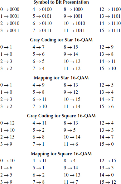
where fc is the frequency of the optical carrier. The coding and mapping bits [D1,D0] into I and Q and the signal constellation points follow the rule shown in Table 7.1.

FIGURE 7.10 (a) Block diagrams of CSRZ-DPSK transmitter and (b) generation of optical pulse with alternative phase by driving the dual-drive MZIM with a 2Vπ, voltage swing.
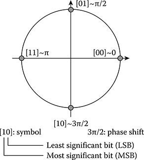
FIGURE 7.11 DQPSK signal constellation.
The DQPSK receiver uses two sets of MZ delay interferometers (DIs) and balance receivers to detect in-phase (I) and quadrature-phase (Q) components of the received signal. Each set is similar to the one used in the NRZ-DPSK receiver. There are, however, two main differences: first, the delay introduced in the first branches of interferometers is now replaced by the symbol duration Ts; second, the phases of the signal in the second branches are shifted by +π/4 and −π/4 for I and Q components, respectively. These additional phase shifts are needed to separate the two orthogonal phase components I and Q.

FIGURE 7.12 (a) Parallel structure of DQPSK transmitter using I–Q modulator and (b) self-homodyne optical receiver for DQPSK signal sequence. Ts = symbol duration.
TABLE 7.1
DQPSK Signal Bit-Phase Mapping
| D1 | D0 | I | Q | Phase Shift |
| 0 | 0 | 0 | 0 | 0 |
| 0 | 1 | 0 | 1 | π/2 |
| 1 | 1 | 1 | 1 | π |
| 1 | 0 | 1 | 0 | 3π/2 |
The spectra of typical NRZ-DQPSK and RZ-DQPSK are shown in Figure 7.13. Likewise, the spectra for the modulation formats of 67% RZ-DQPSK, CSRZ-DQPSK, and 16 MAPSK are shown in Figure 7.14. Figure 7.13a shows the spectrum of the 40 Gbps NRZ-DQPSK signal with the single-sided bandwidth of the main lobe equal to 20 GHz, which is only half of the transmitted bit rate. The spectrum of the RZ-DQPSK signal, Figure 7.13b, is much broader with strong harmonics beside the main lobe.

FIGURE 7.13 Optical spectra of 40 Gbps (a) NRZ-DQPSK, (b) 50% RZ-DQPSK, and (c) DPSK as compared with MSK (dotted curve).

FIGURE 7.14 Optical spectra of 40 Gbps (a) NRZ-DQPSK, (b) 67% CSRZ-DQPSK, and (c) 100 Gbps CSRZ 16-ADPSK.
Despite numerous advancements in optical modulation techniques, the number of levels encoded in a signal symbol falls far behind the 256 or 1024 achieved in microwave modulation schemes [6]. The phase noise associated with optical sources and OAs have hindered the use of phase-related modulation schemes to current fluctuations in the photodetection, and hence the degradation of the BER. The differential phase demodulation process based on the phase comparison of two consecutive symbols requires that the phase should remain stable over two symbol periods. Thus, narrow-linewidth lasers are critical for phase-modulated systems. It has been shown that to achieve a power penalty less than 1 dB [22], Δv/B < 1% with Δv and B, the laser linewidth and system bit rate, respectively. In optical transmission systems where OAs are used, the ASE noise intermingles with the fiber nonlinear phase effect, and thus enhances the nonlinear phase noise. While SPM-induced nonlinear phase noise is the dominant phase noise in single optical channel systems, XPM-induced phase noise is the main phase noise for multichannel (WDM) systems.
Significant phase noise caused by optical sources and OAs have prevented optical DPSK schemes from having many levels in each symbol. Increasing the number of levels in the signal space, and hence the number of bits per symbol higher than one, the most popular solution is a combination of the DQPSK and ASK modulation formats.
Figure 7.15 shows a typical eye diagram for multilevel MAPSK with an amplitude detection section of 40 Gbps after transmission of 5 km SSMF and under only quadrature-phase detection.
Recently, Hayase et al. [9] have demonstrated experimentally a 30 Gbps eight-states per symbol optical modulation system using a combined ASK and DQPSK modulation scheme as shown in Figure 7.16 [6,9]. It maps three bits into a symbol, and thus creates a transmission bit rate that is three times higher than the symbol rate. The transmitter consists of two cascaded PMs and an amplitude modulator (AM). The first PM, driven by data bit D0, creates 0 and π phase shifts, while the second, driven by D1, forces two further phase shifts 0 and π/2, the quadrature phase to generate four distinct phases of the DQPSK signal. The AM, driven by D2 bit, shifts the four phases between two amplitudes to create totally eight signal points.
At the receiver side, optical signals are detected in both amplitude and differential phase. An ASK demodulator detects the D2 bit. The other is a DQPSK demodulator and detected to recover D1 and D0 bits. Sekine et al. [6] reported experimentally a similar scheme, but with four bits [D3,D2,D1,D0] mapped into a symbol: [D1,D0] bits are used to generate a “normalized” DQPSK signal, while [D3,D2] bits manipulate the amplitude of this DQPSK signal between four concentric circles. Thus, a 16-ary MADPSK signal can be generated. This would offer 40 Gbps bit rate with a symbol rate of only 10 GBauds.
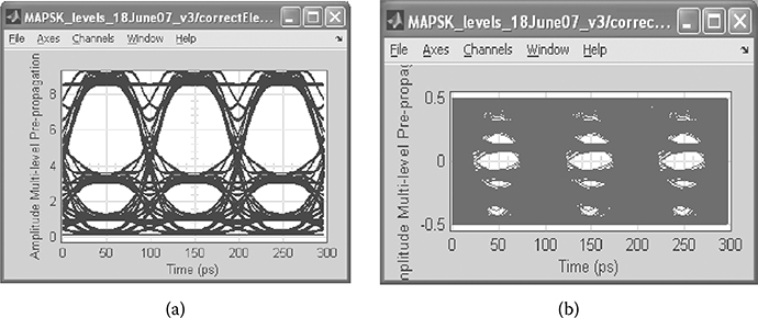
FIGURE 7.15 Eye diagram showing amplitude detection section of 40 Gbps. (a) 5 km SSMF transmission and (b) quadrature-phase detection.

FIGURE 7.16 8-ary APSK modulation experimental configuration (Extracted from K. Sekine et al., IEEE Electron. Lett., Vol. 41, No. 7, 2005.), 10 GHz clock assignment synchronization of symbol rate, data modulator, and quadrature-phase shift in optical domain using the PM, two balanced receivers for differential phase shift detection and direct detection for amplitude detection. (a) 8-ary ASK-DPSK signal, (b) transmitter configuration, and (c) receiver configuration. (Adapted from S. Hayase et al., Proposal of 8-state per symbol (binary ASK and QPSK) 30-Gb/optical modulation demodulation scheme, Proc. European Conf. Opt. Commun., paper Th2.6.4, ECOC 2003, Rimini, Italy, pp. 1008–1009, September 2003.)
7.2.3 Comparison Of Different Amplitude And Phase Optical Modulation Formats
Different amplitude and phase optical modulation formats are summarized in Table 7.2. In most cases, NRZ-ASK parameters are used as references. From the comparison, it can be concluded that MADPSK is advantageous compared to other modulation formats in terms of spectral efficiency and the ability to significantly increase the transmission bit rate, which are very, if not the most, important parameters for an optical transmission system. It is also expected that MADPSK inherits good properties (and of course the bad ones, if any) from two basic ASK and DPSK modulation formats.
TABLE 7.2
Comparison of Different Optical Modulation Formats.

7.2.4 Multilevel Optical Transmitter Using Single Dual-Drive MZIM Transmitter
In this section, several optical transmitter structures used for generating the DQPSK signal are described. This is necessary because a novel optical transmission system will be developed based on the DQPSK modulation format. All these structures have MZIM as their base component, which can be a single- or dual-electrode structure. Figure 7.11 displays a constellation of QPSK modulation.
Unlike a single-drive MZIM, a dual-drive electrode structure with two traveling wave RF electrodes can modulate the phase of optical signals in both branches, and hence push–pull operation. Interference at the output of a dual-drive MZIM will produce a phase-modulated signal. However, when the effects of phase modulation in the two branches are exactly equal but opposite in sign, the output signal becomes intensity modulated. In this manner, a dual drive can be used for both phase and intensity modulation. The relationship between the input and output signals of a dual-drive MZIM can be described by [12,23]
where V1(t) and V2(t) are the driving voltages applied to the modulator, and Vπ is the voltage required to provide a π phase shift of the carrier in each branch of MZIM. Note that unlike in single-drive MZIMs, the chirp effect does not exist in dual-drive MZIMs.
The transmitter structure shown in Figure 7.12 is called the parallel type. It is only one of several structures that can be used for generating the DQPSK signal, namely, parallel structure, serial structure, single PM structure, and dual-drive MZIM structure. These terms are used to indicate the structuring of MZIMs whether they are connected in tandem, parallel, or just a pure PM with a single electrical drive port.
In an electro-optic transmitter of the serial type shown in Figure 7.17, an MZIM generating an in-phase component and a PM generating a quadrature component are connected in tandem. Pre-encoded data generate two signals: one is used for driving the MZIM and the other for driving the PM. Usually, the square shape of the precoded waveforms is replaced by the raised-cosine one before being fed to the modulators [21]. Furthermore, the biasing conditions and the amplitude of the modulators can be used to generate 33% to 67% pulse width RZ formats. It is also noted that the pulse shape would also follow a cos2 profile owing to the property of the IM. This transmitter would suffer from the chirping effects owing to the rise time of the electrical driving signals and hence would contribute to the distortion of the lightwave signals, in particular when switching between the lowest level to the highest level.
The single PM structure shown in Figure 7.18 uses only one MZIM as the PM. Precoded data are added up to create a single driving voltage. One of the two precoded data is amplified and together with the other signal represents four positions of the DQPSK signal [21].
The dual-drive MZIM structure in Figure 7.19 uses two driving voltages for modulating the optical carrier phase in two branches of an MZIM. Data are first precoded following the differential rule and then used to create driving voltages V1(t) and V2(t) corresponding to the signal constellation points [21].

FIGURE 7.17 Cascade PM and MZIM for DQPSK signal generation.

FIGURE 7.18 Single PM structure.

FIGURE 7.19 Dual-drive MZIM structure.
In the four transmitter structures described earlier, the parallel and serial structures are the most complex and difficult to implement because they have discrete devices connected together. The dual-drive MZIM and single PM structures, on the contrary, are much simpler because they require fewer discrete devices. Furthermore, as will be shown in the next section, dual-drive MZIMs can be configured to work as both PM and AM at the same time, so they can easily generate not only DQPSK but also MADPSK signals. Thus, a dual-drive MZIM is the principal part of the MAPSK transmission system. Table 7.3 gives a comparison between the different transmitter structures; the dual-drive modulator is outstanding for combined amplitude and phase switching between the states of a multicircular constellation.
The main reason why the dual-drive MZIM structure has attracted our attention in this chapter is that it can play the role of both AM and PM simultaneously, which is impossible with other transmitter structures. This means that to generate an MADPSK signal, there is no need to employ separate PM and AM, as has been implemented by Sekine et al. [6] and Hayase et al. [9]. This section describes a method for generating a 16-ary MADPSK signal using this dual-drive MZIM structure.
The 16-ary MADPSK signal constellation of interest is shown in Figure 7.20. It is actually a combination of a 4-ary ASK and a DQPSK signal, with four bits [D3,D2,D1,D0] mapped into a symbol. Among them, two bits [D1D0] are coded into four phases [0,π/2,π,3π/2], and two bits [D3D2] are coded into four amplitude levels [I3,I2,I1,I0]. As has been shown in Ref. [6], with the use of a balanced receiver and a DI.
The MADPSK signal sequence can produce clear DQPSK eye patterns whose decision level is located at the zero-voltage level.
Recall that the signal at the output of the dual-drive MZIM can be represented as [12,23]
with , where Ei and Eo are electrical fields of the input and output optical signal, respectively; V1(t), V2(t) are driving voltages applied to the modulator; and Vπ is the voltage required to provide a π phase shift for the carrier in each MZIM branch.
Equation 7.5 suggests that with a properly chosen input signal Einput and driving voltages V1(t), V2(t), all signal points of the constellation in Figure 7.20 can be constructed from two phasor signals and . Indeed, if Ei is chosen to equal the electrical field corresponding to the signal points in the largest circle of the constellation, then a constellation signal point Eoutput with the phase shift θi in the circle n can be found as a sum of two vectors and , where ϕni1 = θi + arccos(En/Einput), ϕni2 = θi + cos(−1En/Ei). The subscriptions i and n are used to denote the phase position and the order of the circle of interest. Figure 7.21 illustrates the relationship between Ei, E0, ϕni1, and ϕni2. For simplicity, the signal point is chosen with θi = 0.
TABLE 7.3
Comparison of DQPSK Transmitter Structures.
| Parameters for Comparison | Parallel MZIM | Serial MZIM & PM | Single PM | Dual-Drive MZIM |
| Complexity of circuit design | Complicated in matching of ultra-high-frequency electrical paths; high insertion loss. Flexible in biasing. | Complicated in matching of ultra-high-frequency electrical paths; high insertion loss. Flexible in biasing. | Simple in photonics but complicated in realization of ultra-high-frequency signal connections. | Simplest but requires multilevel voltage switching at symbol rate (microwave speed). |
| Ability to create MADPSK signal | Not possible. A separate ASK modulator required. | Not possible. A separate ASK modulator required. | Impossible. A separate ASK modulator required. | Dual-drive MZIM acts as ASK and DPSK simultaneously. |
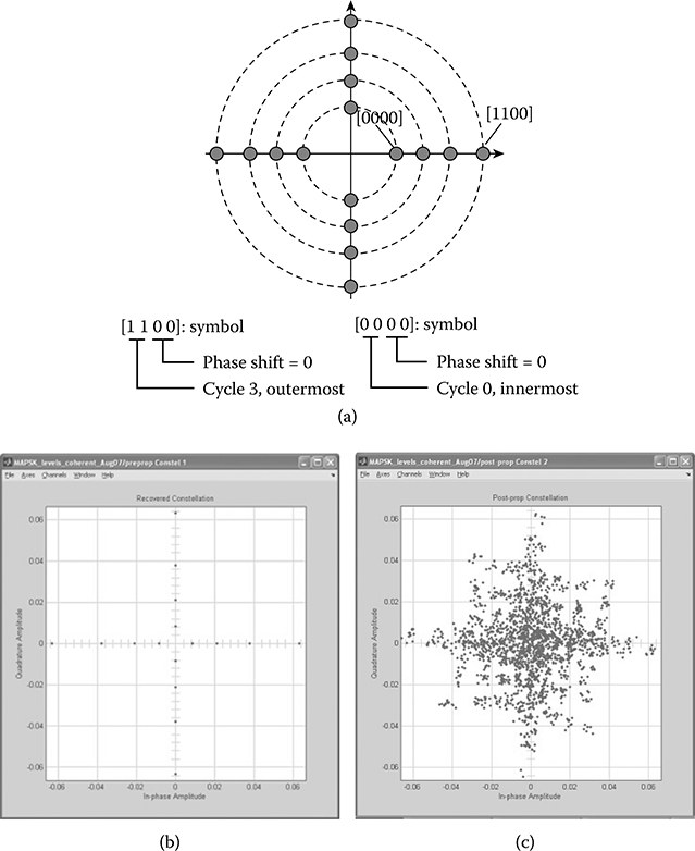
FIGURE 7.20 16-ary MADPSK signal bit-phase mapping: (a) design, (b) Simulink® scattering plot before transmission, and (c) after 200 km transmission with 2 km mismatch in dispersion.
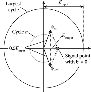
FIGURE 7.21 Relationship between Ei E0, ϕni1, and ϕni2 using phasor representation.
By substituting ϕ1 and ϕ2 in Equation 7.5, the driving voltages for this point can be obtained
7.3 MADPSK Optical Transmission
In general, the structures of the MADPSK can be given as shown in Figure 7.22. A model has been constructed for investigating the performance of systems based on the MADPSK modulation format. It consists of a signal coding model, transmitter model, receiver model, and transmission and dispersion compensation fiber models.
The 16-ary MADPSK signal model described in Section 7.2 will be used. To balance the ASK and DQPSK sensitivities, ASK signal levels are preliminary adjusted to the ratio I3/I2/I1/I0 = 3/2/1.5/1 [6]. as shown in Figure 7.23. These level ratios can be determined from the signal-to-noise ratio at each separation distance of the eye diagram or Q factor. The noise is assumed to be dominated by the beat noise between the signal level and that of the ASE noise.
The transmitter model shown in Figure 7.24 is used to produce the 16-ary MADPSK signal. It consists of a DFB laser source generating continuous wave (CW) light (carrier), which is then modulated in both phase and amplitude by a dual-drive MZIM. Each of the four bits of user data [D3D2D1D0] is first grouped into a symbol and then encoded to generate two electrical driving signals V1(t) and V2(t) under which the amplitude and phase of the carrier in two optical paths of the dual-drive MZIM will be modulated to produce the NRZ 16-ary MADPSK signal. The RZM-PC then converts the NRZ pulse train into RZ one in order to minimize the effects of intersymbol interference.
The receiver model shown in Figure 7.25 consists of two phase demodulators, an amplitude demodulator and a data multiplexer MUX. Two phase demodulators are used for extracting the [D1D0] bits, and they work exactly in the same way as the ones in the DQPSK receiver described in the foregoing section. The amplitude demodulator (AD) is used for detecting four amplitude levels of the MADPSK signal. It is a well-known direct detection scheme consisting of a photodiode followed by an electronic receiver. The amplitude modulated signal is then threshold detected in association with a clock recovery circuit to recover two bits [D3D2]. The two bits [D3D2] are interleaved with the two bits [D1D0] by the MUX to reconstruct the original binary data stream.

FIGURE 7.22 Schematic diagram of the photonic transmitters and receivers for the 16ADQPSK transmission scheme: (a) transmitter and (b) receivers with branches for detection of amplitude, in-phase and quadrature-phase components.
7.3.1 Performance Evaluation
Under performance evaluation, the following main parameters are investigated:
The system bit error rate (BER) versus SNR: A solution for the system BER will be found analytically, and the BER will be computed against different SNR values and bit rates. The system BER versus the SNR will also be obtained by system simulation and crosschecked with the BER against that obtained analytically. Graphs of BER versus SNR will be plotted.
The system BER versus receiver sensitivity: The BER versus receiver sensitivity will be obtained analytically and by simulation, and the results will be cross checked. Graphs of BER versus receiver sensitivity will be plotted.

FIGURE 7.23 ASK interlevel spacing.
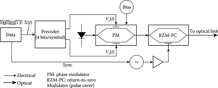
FIGURE 7.24 MADPSK transmitter.

FIGURE 7.25 Amplitude direct detection and photonic phase comparator with balanced receiver for MADPSK demodulation.
Dispersion tolerance: Transmission over fibers of types ITU-G652, ITU-G.655, and LEAF with corresponding dispersion factors will be considered. Graphs of the power penalty due to the dispersion as compared with back-to-back transmission will be plotted against the dispersion factor in ps/nm.
Tolerance to other system impairments: For example, with dispersion tolerance (DT), the power penalty due to other impairments such as laser and OA phase noise, and receiver phase error will be investigated. The corresponding graphs will be plotted.
Performance evaluation is conducted under the effects of the following conditions or contexts:
Different pulse shapes: raised cosine, rectangular, and Gaussian
Modulation formats: NRZ, RZ, and CSRZ
ASE noise of OAs
Transmitter impairments: laser noise
Receiver impairments: phase error of DI-based phase demodulators
Change of ASK interlevel spacing
Optical and electrical filtering
Multichannel environment: system performance in combination with DWDM technology would be reported in future
7.3.2 Implementation of MADPSK Transmission Models
The following simulation models have been built on the MATLAB and Simulink platform for proving the working principles and for investigating the performance of systems using optical MADPSK modulation. A transmitter is simulated to generate a 16-ary MADPSK signal, and a receiver is to reconstruct the original binary signal. These models run over a simulated single-mode optical fiber. Laser chirp, OA phase noise, nonlinearities, CD, PMD, and other impairments will be involved in later stages to evaluate the different performance characteristics of the modulation format: system BER, receiver sensitivity, and power penalties due to different impairments.
The phases and the driving voltages for creating the signal points of the 16-ary MADPSK constellation are computed and tabulated in Table 7.4.
7.3.3 Transmitter Model
The MATLAB and Simulink model of the system is shown in Figure 7.26.
The transmitter model using the dual-drive MZIM structure is shown in Figure 7.27. The purpose of the blocks are as follows:
The User Data and ADPSK precoder block generates a pseudo-random data sequence to simulate user data stream and encodes each group of four data bits into a symbol.
The Voltage driver 1 and Voltage driver 2 blocks map precoded data into driving voltages for modulating the amplitude and phase of the carrier in the dual-drive MZIM.
Two Complex Phase Shift blocks simulate two optical paths of the dual-drive MZIM.
The Sum block simulates the combiner at the output of the MZIM.
The Gaussian Noise Generator block simulates a noise source.
The Amplifier block simulates an OA.
7.3.4 Receiver Model
The receiver structure is shown in Figure 7.28.
TABLE 7.4
Phase and Driving Voltages for 16-Ary MADPSK Constellation

The functions of the blocks are as follows:
Each DI is simulated by a set of two Magnitude-Angle blocks, a Delay block and a Sum block. The Delay block stores the phase of the previous symbol, and the Magnitude-Angle blocks extract the phase and amplitude of the present and previous symbols, which will be used in the followed different phase demodulation and detection operations.
The Constant π/4 and Constant π/4 and the next two Sum blocks simulate an extra phase delay in each branch of the DI.
Two Cos blocks and two Product blocks simulate two balanced receivers.
The Amplitude Detectors, D2 and D3 blocks, simulate the ASK detector for D2 and D3 bits.
Three Analog Filter Design blocks simulate electrical low-pass filters.
The Phase Detector D0_I and Phase Detector D1_Q blocks simulate the threshold detectors for D0 and D1 bits (I and Q components of a DQPSK signal), respectively.
7.3.5 Transmission Fiber and Dispersion Compensation Fiber Model
The propagation of an optical signal in a fiber medium that is dispersive and nonlinear is best described by the nonlinear Schrödinger equation (NLSE) [22] as described in Chapter 2. Other parameters are explained in the following text. The transmission fiber model shown in Figure 7.29 is used to simulate the propagation of an optical signal. This fiber model simulates the impairments that impact the system performance.
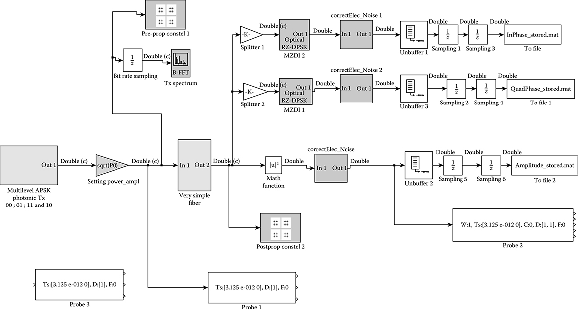
FIGURE 7.26 MATLAB® simulated system model.
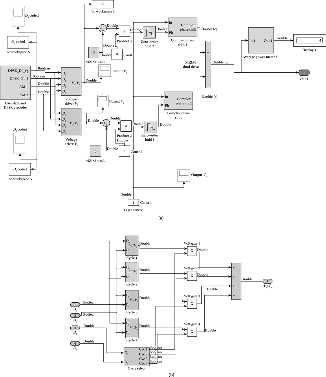
FIGURE 7.27 MATLAB® simulated MADPSK: (a) transmitter. MATLAB® simulated MADPSK: (b) logic precoder.

All characteristic parameters of the fiber medium together with the optical input signal are taken by the Matrix Concatenation block and then processed by a MATLAB function that solves the NLSE using the split-step Fourier method [24].
The dispersion compensation fiber model has the same structure as the propagation fiber model, except that the signs of the propagation constant beta2 in the two models are opposite.
7.3.6 Transmission Performance
7.3.6.1 Signal Spectrum, Signal Constellation, and Eye Diagram
The spectrum of a 40 Gbps 16-ary MDAPSK signal obtained by the running transmitter model is given in Figure 7.30. As is seen clearly in the graph, the single-sided bandwidth of the main lobe equals 10 GHz. Numerically, this amounts to only one-fourth of the transmission bit rate, and from that it can be concluded that MADPSK is a high bandwidth-efficient modulation format.
Figure 7.31 shows the signal constellation recovered at the receiving end. The noise and nonlinear property of the fiber cause amplitude and phase fluctuations and scatter signal points around some mean value. The MADPSK eye diagram is shown in Figure 7.32 for the I component (the Q component should have a similar diagram). This eye diagram clearly shows four amplitude levels associated with the two phase shifts 0 and π.
7.3.6.2 BER Evaluation
The MADPSK system can be considered as consisting of two subsystems, ASK and DQPSK, and its error probability can be evaluated as a joint error probability of the two
where PASK and PDPSK are the error probabilities of the ASK and DQPSK subsystems, respectively.
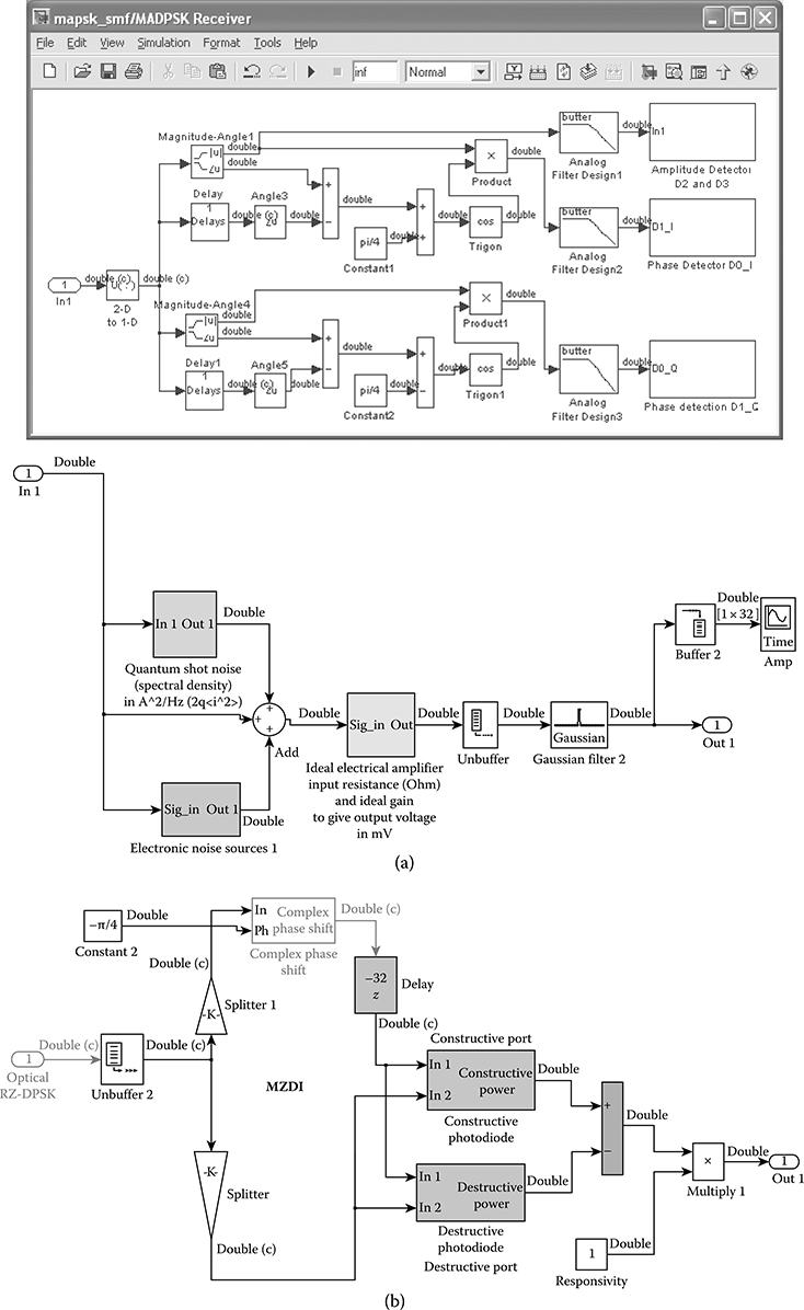
FIGURE 7.28 MATLAB® simulated MADPSK receiver: (a) amplitude direct detection and (b) balanced receiver detection—in-phase and quadrature.
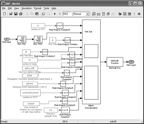
FIGURE 7.29 Single-mode fiber model.
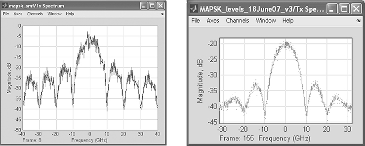
FIGURE 7.30 40 Gbps MADPSK spectrum.

FIGURE 7.31 40 Gbps MADPSK constellation recovered at the receiver.

FIGURE 7.32 40 Gbps MADPSK eye diagram at OSNR = 20 dB: (a) NRZ amplitude, (b) CSRZ amplitude, (c) NRZ in phase, and (d) CSRZ in phase.
7.3.6.3 ASK Subsystem Error Probability
Figure 7.33 shows four ASK signal levels b0, b1, b2, b3, three decision levels d1, d2, d3, and the standard deviation of noise at different signal levels σ0, σ1, σ2, σ3.
The error probability of the ASK subsystem can be evaluated by [25]
For example, in our system: (1) b1 = 8.08e − 2, b2 = 1.45e − 1, b3 = 2.42e − 1, (2) d1 = 5.11e − 2, d2 = 1.08e − 1, d3 = 1.88e − 1, (3) σ1 = 5.00e − 3, σ2 = 6.70e − 3, σ3 = 8.85e − 3 at an OSNR = 20 dB.
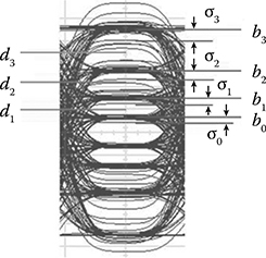
FIGURE 7.33 MADPSK eye diagram: signal levels, decision levels, and standard deviation of noise.
The error probability of the ASK subsystem thus equals
The error probability of the ASK subsystem over a range of OSNR from 6 to 24 dB is evaluated and shown in Figure 7.34.
7.3.6.4 DQPSK Subsystem Error Probability Evaluation
In terms of differential phase shift keying modulation, the system can be broken up into four independent DQPSK subsystems corresponding to circle 0, circle 1, circle 2, and circle 3 of the signal constellation. The error probability of each subsystem is evaluated first, and then they are averaged to obtain the error probability of the DQPSK subsystem.
Each DQPSK subsystem in turn can be thought of as being made up of two 2-ary DPSK subsystems. The error probability of each 2-ary DPSK subsystem is evaluated, and then they are averaged to get the error probability of the DQPSK subsystem
where PDPSK_I and PDPSK_Q is the error probability of the in-phase (I) and quadrature-phase (Q) components of each DPSK subsystem (circle). Because I is coded by bit D0, Q is coded by bit D1, I and Q are detected in the same way, and D0 and D1 are supposed to be equally probable, then (20) becomes
PDPSK_I is evaluated based on the δ-factor [22]

FIGURE 7.34 Error probability of ASK subsystem versus OSNR.
where , iH, iL and σH, σL are the mean value and standard deviation of signal currents at high and low levels at the input of the receiver, respectively. For example, the transmission parameters can be set as follows: iH = 3.23e − 02, iL = (−3.23e − 02), at OSNR = 20 dB σH = σH = 3.16e − 3. The δ-factor for a single DQPSK subsystem of circle 0 thus equals, and the corresponding error probability is
The error probability of circle 0 (the innermost circle) is PDQPSK_CYCLE0 = 2 ∗ (7.7e − 24) − (7.7e − 24)2 = 1.54 ∗ 10e − 23. Thus, the error probability of all four circles is
PDQPSK over a range of OSNRs from 6 to 24 dB is evaluated and shown in Figure 7.35.
7.3.6.5 MADPSK System BER Evaluation
The MADPSK system error probability is evaluated based on Equation 7.17. Figure 7.36 shows the graphs of the error probability for the ASK subsystem, DQPSK subsystem, and MADPSK system in the same coordinates for comparison purpose. As can be observed from Figure 7.36, at OSNR = 24 dB, the MADPSK. It is also clear that for the same value of the OSNR, especially when it is high, the DQPSK subsystem outperforms its ASK counterpart, and the overall performance of the MADPSK system is dominated by the ASK subsystem performance. Thus, the spaces between the ASK levels could be adjusted for a better balance between the BER ASK and the BER DQPSK to achieve a better overall MADPSK BER performance. This probably is caused mainly by the intersymbol interference during the transition of different levels.

FIGURE 7.35 Error probability of DQPSK subsystem versus OSNR.

FIGURE 7.36 Error probability of MADPSK (black) system versus OSNR; logarithm scale. Error probability of ASK (light gray) and MADPSK almost coincide.
Figure 7.36 shows the simulation results of 16ADPSK at 100 Gbps transmission (extreme left graph) in comparison with other modulation formats such as Duobinary 50 and Duobinary 67 and experimental results of CSRZ-DPSK. The bit rates of these other transmission results are at 40 Gbps. It is observed that for 16MADPSK, the receiver sensitivity is close to the −28 dBm performance standard used in 10 Gbps NRZ transmission, and performs better at 100 Gbps than the other modulations operating at the lower rate of 40 Gbps. However, this superior performance at 100 Gbps is still with a penalty of approximately 3 dB compared with 10 Gbps transmission systems. Fortunately, this penalty can easily be compensated for by using a low-noise optical preamplifier at the receiver end. For example, a 15 dB gain optical preamplifier with a 3 dB noise figure would satisfactorily resolve the issue. The BER versus the receiver sensitivity of 16ADPSK and duobinary formats and ASK are shown in Figure 7.37. It indicates a 2–3 dB improvement of the MADPSK.

FIGURE 7.37 BER versus receiver sensitivity for MADPSK format and other duobinary and ASK ( simulation) and CSZ and CSRZ-DPSK (experimental). Legend: mid gray * is the MDAPSK.
The detection of the lowest level may have been affected by the noise level of the optical preamp when only the amplitude information is used. This can be improved significantly if both phase detection and amplitude detection are used, as is observable from Figure 7.32c and d.
7.3.6.6 Chromatic DT
The residual CD of the optical link is characterized by the DL product, which is defined as the product of the dispersion coefficient D and the total fiber length L. Figure 7.38 shows the signal phase evolution under the effect of CD. It can be seen that with a predetermined DL = 50 ps/nm, all signal points are rotated around the [0,0] origin by the same angle of approximately 0.125 rad. This confirms the parabolic phase shift due to the CD. This phenomenon is called linear phase distortion, in contrast to the nonlinear phase distortion caused by the fiber nonlinearity.
Figure 7.39 shows the BER penalty versus different values of the DL product. It can be seen very clearly that the BER performance of the NRZ format is severely affected by the fiber dispersion. When the DL increases from 0 ps/nm (fully CD compensated) to 35 ps/nm, its BER performance is improved by 1.5 dB, but sharply degraded by a 28 dB penalty at DL = 50 ps/nm, and should be worse for a higher value of dispersion. This leads to the conclusion that it is undesirable to use the NRZ format in MADPSK systems because the optical link residual dispersion usually cannot be compensated to a small amount, and an ineffective dispersion management and control plan could lead to a very high BER.
The 66%-RZ format, on the contrary, can tolerate a much higher degree of CD. Its BER performance is even slightly improved at DL ≈ 50 ps/nm, and the BER penalty is less than 1 dB at DL = 100 ps/nm. This is equivalent to the transmission over 6 km of uncompensated standard SMF fiber without significantly compromising the BER performance.
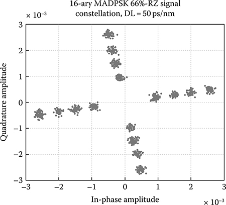
FIGURE 7.38 Evolution of the phase scattering of the MADPSK signal constellation under chromatic dispersion effects.

FIGURE 7.39 Error probability of MADPSK system versus the dispersion-length DL product.
The MAPSK offers a lower symbol rate and hence a higher channel capacity that would allow the upgradation to a higher rate over a low-bit-rate optical fiber transmission system without modifying the photonic infrastructure of the optical networks.
7.3.6.7 Critical Issues
This section outlines the critical issues involved in the evaluation of the performance of MADPSK systems.
7.3.6.7.1 Noise Mechanism and Noise Effect on MADPSK
Although receiver noise in multilevel amplitude modulation was investigated intensively in the 1980s, little has been reported for multilevel phase and differential phase modulation. One of the principal goals in the system design, especially for long-haul transmission systems, is to achieve high receiver sensitivity. At a given optical power, the error probability depends on the noise power, and hence the receiver sensitivity.
Quantum shot noise is the fundamental noise mechanism in photodiodes, which leads to a fluctuation in the detected electrical current even when the incident optical signal has a constant or variable power. Thus, it is signal dependent. Furthermore, the beating of the currents of the signal and the optical phase noise would generate an amplitude-dependent noise at different-level signals of the MADPSK. It is caused by random generation of electrons contributing to the photoelectric current, which is a random variable. All photodiodes generate some current even in the absence of an optical signal because of the stray light and/or thermal generation of electron–hole pairs, the dark current.
In MADPSK, the amplitude of the signal of the outermost circle of the constellation would be affected by the quantum shot noise, which is strongly signal amplitude dependent, especially when there is an optical preamplifier. On the contrary, it is desirable that the innermost constellation would have the largest magnitude to maximize the optical signal energy for long-haul transmission. Therefore, an optimum receiving scheme must be developed both analytically and by modeling and eventually by experimental demonstration.
However, the amplitude of the outermost constellations is limited by the nonlinear SPM effects, which will be further explained in the next few sections. Thus, the lower and upper limits of the amplitude of the MADPSK would be extensively investigated in the next phases of the research.
The electronic equivalent noise as seen from the input of the electronic preamplifier following the photodetector can be measured and taken into account for the total noise process caused by the thermal noise of the input impedance, the biasing current shot noise, and the noise at the output of the electronic preamplifier. These noises are combined with the signal-dependent quantum shot noise so as to gauge their contribution to the MADPSK receiver. Thus, we may consider new structures of electronic amplifiers or a matched filter at the input of the receiver to achieve the optimum MADPSK receiver structure.
For long-haul transmission systems, the ASE of an OA is probably the most important noise mechanism. In OAs, even in the absence of an input optical signal, spontaneous emission always occurs stochastically when electron–hole pairs recombine and release energy in the form of light. This spontaneous emission is noise, and it is amplified by the OAs together with the useful optical signal and accumulated along the optical transmission link [26].
Noise reduces the SNR, and hence the system BER and receiver sensitivity. Noise models also affect the design of optimum detection schemes such as decision thresholds. To the best of my knowledge, a thorough investigation of the noise mechanism and its impact on multilevel signaling has never been reported except some preliminary results for 10 Gbps 4-ary ASK schemes [10]. Thus, all noise sources and the mechanism by which they affect the system performance must be thoroughly investigated. These noises are used to estimate the optimum decision level of the detection of the amplitude of the multilevel eye diagram (Figure 7.40).
7.3.6.7.2 Transmission Fiber Impairments
For optical signals, the transmission medium is an optical fiber with associated OAs and dispersion compensation devices, or a leased wavelength running on top of a DWDM system. Impairments are always part of the transmission medium; among them, CD, PMD, and nonlinearity are critical.
When an optical pulse propagates along a fiber, its spectral components disperse owing to the differential group delay (DGD), and the output pulse will be broadened. CD is proportional to the fiber length and the laser linewidth, especially the spectrum of the lightwave modulate signals.

FIGURE 7.40 ASK interlevel spacing and offset modulation and detection line.
CD may cause optical pulses to overlap each other, thus leading to intersymbol interference, and increase the system BER, especially for ASK systems. DPSK systems, on the contrary, are more CD tolerant. For MADPSK systems, the eye diagrams and phase constellation are as shown in Figures 7.41 and 7.42, respectively. The phase constellation is rotating when the MADPSK is under the linear CD effect. Another idea that is well known—and is developed in our model—is that this CD can be compensated by dispersion-compensating fiber modules. However, the mismatching of the dispersion slopes of the transmission and compensating fibers is very critical for multichannel multilevel modulation schemes.
The optical pulse is also broadened by PMD, which is actually the time mismatch between two orthogonal polarizations of the optical pulse when they traverse along a fiber. In the ideal optical fiber having a truly homogeneous glass and a truly coaxial geometry of the core, the two optical polarizations would propagate with the same velocity. However, this is not the case for a real fiber, so the two polarizations have different speeds and will reach the fiber end at different times.
Similar to the CD effects, PMD can cause pulse overlapping and thus increase the system BER. However, unlike CD, which is practically constant over time and can be in a large scale compensated, PMD is a stochastic process and cannot be managed easily. It is well known that PMD has the Maxwellian probability density function with a mean value , where KPMD is defined as a PMD coefficient whose measured values vary from fiber to fiber in the range , and L is the fiber length. Under the MADPSK, the signal space of the constellations would be affected either in the magnitude or phase by PMD, but is expected to be dominated by the phase distortion. It is well known that the PMD first and second effects are critical for ASK modulation. For DPSK, it is expected that the principal axes of the polarization modes propagating through the fiber would be minimally affected. Thus, under the hybrid amplitude–phase modulation scheme, several issues remain to be resolved. Under the MADPSK scheme, the delay of the polarization modes would generate the phase difference or phase distortion on the I and Q components, and hence an enhancement of the distortion effects of the ISI. The amplitude distortion would then be increased but is considered to be a secondary effect.
7.3.6.7.3 Nonlinear Effects on MADPSK
Nonlinear effects occur owing to the nonlinear response of the fiber glass to the applied optical power. Fiber nonlinearity can be classified into stimulated scattering and the Kerr effect. Among several stimulated scattering effects, stimulated Raman scattering, caused by the interaction between light and the acoustical vibration modes in the fiber glass, is the most critical. Under this mechanism, the optical signal is reflected back to the transmitter, and in WDM systems its power is also transferred from shorter to longer wavelengths, thus attenuating the signal and causing crosstalk. The Kerr effect is the cause of the intensity-dependent phase shift of the optical field. It manifests in three forms: self-phase modulation (SPM), cross-phase modulation (XPM), and four-wave mixing (FWM) provided the phase matching is satisfied.

FIGURE 7.41 40 Gbps MADPSK eye diagrams of the (a) I and (b) Q components (A) 0 km—back-to-back, (B) 2 km SSMF mismatch over three 100 km SSMF transmission spans (dispersion compensated).

FIGURE 7.42 Constellation of 16-square QAM after two optically amplified spans and 2 km SSMF dispersion mismatch: (a) prepropagation and (b) postpropagation.
SPM is usually the dominant effect in a single-channel DPSK system. The changes in instantaneous power of the optical pulses together with the ASE from associated OAs lead to intensity-dependent changes, the Kerr effect, in the guided medium refractive index, and hence the effective index of the guided mode. These changes are converted to the phase shifts or phase noise of the lightwave carriers. At the receiver, the phase noise is transferred back to intensity noise, which degrades the BER [27]. As mentioned earlier, the contribution of noise to different levels of the MADPSK scheme is very critical to determine the optimum decision thresholds. This is further complicated by these additional nonlinear effects, especially the nonlinear phase noise (NLPN) usually contributed by the SPM due to the outermost constellation. These NLPN effects from the outermost constellation to other inner circle signal spaces have never been investigated.
XPM becomes the most critical nonlinearity in WDM systems where the phase shifts (noise) in one channel comes from refractive index fluctuations caused by power changes in other channels. XPM becomes more pronounced when neighboring channels have equal bit rates [27]. FWM is basically a crosstalk phenomenon in WDM systems. When three wavelengths with frequencies, ω1, ω2, and ω3 propagate in a nonlinear fiber medium at which the dispersion is zero, they combine and create a degenerate fourth wavelength that would fall in an active wavelength channel. If these parametric wavelengths fall in other channels, they cause crosstalk and degrade the performance of the system. Although FWM is expected to reduce the receiver sensitivity, in the proposed system, to minimize the effects of fiber nonlinearity, the maximum power of the optical signal should not be set higher than a certain threshold. This maximum power dictates the amplitude of signal points in the outermost circle (circle 3), and hence other circles, of the signal space. Thus, optimization of the signal amplitude levels for MADPSK is critical.
7.3.6.8 Offset Detection
The 16-ary MADPSK signal model described in Section 7.3.2 can be modified. To balance the ASK and DQPSK sensitivities, the ASK signal levels are preliminary adjusted to the ratio I3/I2/I1/ I0 = 3/2/1.5/1 and rotated by π/4 [6] as shown in Figure 7.40. These level ratios can be determined from the signal-to-noise ratio at each separation distance of the eye diagram or Q factor. The noise is assumed to be dominated by the beat noise between the signal level and that of the ASE noise. The eye opening is expected to improve significantly as shown in Figure 7.41.
7.4 Star 16-QAM Optical Transmission
This section gives a description of the simulation of the transmission performances of optical transmission systems over ten spans of dispersion-compensated and optically amplified fiber transmission systems. The modulation format is focused on the Star 16-QAM with two level and eight phase state constellation. Optical transmitters and coherent receivers are the main transmission terminal equipment; other constellations of the 16-QAM are described very briefly. Simulation results have shown that it is possible to transmit and detect the data symbols for 43 Gbps with the possibility of scaling to 107 Gbps without much difficulty. The OSNR with 0.1 nm optical filters is achieved with 18 and 23 dB for back-to-back and long-haul transmission cases with a DT of 300 ps/nm.
7.4.1 Introduction
To increase the channel capacity and bandwidth efficiency in optical transmission, the multilevel modulation formats such as QAM formats are of interest [43, 44, 45, 46, 47, 48, 49 and 50]. In digital transmission with multilevel (M levels) modulation, m bits are collected and mapped onto a complex symbol from an alphabet with M = 2m possibilities at the transmitter side.
The symbol duration is Ts = mTB with TB as the bit duration, and the symbol rate is fs = fB/m with fB = 1/TB as the bit rate. This shows that for a given bit rate, the symbol rate decreases if the modulation level increases. That means a higher bandwidth efficiency can be achieved by a higher-order modulation format. For the 16-QAM format, m = 4 bits are collected and mapped to one symbol from an alphabet with M = 16 possibilities. In comparison to the case of the binary modulation format, only m = 1 bit is mapped to one symbol from an alphabet with M = 2 possibilities. With 16-QAM format and a data source with a bit rate of fB = 40 Gbps, only a symbol rate of fs = 10 GBaud/s is necessary. From the commercial point of view, this means a 40 Gbps data rate can be transmitted with 10 Gbps transmission devices. In the case of binary transmission, the transmitter needs a symbol rate of fs = 40 GBaud/s. This means 16-QAM transmission requires four times slower transmission devices than that for the binary transmission. It is noted here that 10.7 Gsymbol/s is used as the symbol rate so as to compare the simulation results with the well-known 10.7 Gbps modulation schemes such as DPSK, CSRZ-DPSK, and so on. For a 107 Gbps bit rate, the transmission performance, that is, the sensitivity and the OSNR, can be scaled accordingly without any difficulty.
This section gives a general approach to the design and simulation of Star 16-QAM with two amplitude levels and eight phase states forming two star circles. We term this Star 16-QAM as 2A-8P Star 16-QAM, two amplitude level and eight phase states. The transmission format is discussed with theoretical estimates and simulation results to determine the transmission performance. The optimum Euclidean distance is defined for the design of star 16-QAM. Then in the second Section 7.4.4, the two detection schemes, namely direct detection and coherent detection, for Star QAM constellations are discussed.
7.4.2 Design Of 16-QAM Signal Constellation
There are many ways to design a 16-QAM signal constellation. The three most popular constellations for 16-QAM modulation schemes are (1) Star 16-QAM, (2) Square 16-QAM, and (3) Shifted-square 16-QAM. The first two of these constellations are implemented. However, only the Star 16-QAM with two amplitudes and eight phases per amplitude level are employed in this section.
7.4.3 Signal Constellation
The signal constellation for Star 16-QAM with Gray coding is shown in Figure 7.43. The binary presentation of the symbols in the figure is shown in the symbol to bit presentation mapping of Table 7.5.
As can be seen from the figure, the symbols are evenly distributed on two rings, and the phase differences between the neighboring symbols on the same ring are equal (π/4). In order to detect a received symbol, its phase and amplitude must be determined. In other words, between two amplitude levels of the rings and among eight phase possibilities, there are a number of ways to build this constellation.
The ring ratio (RR) for this constellation is defined as RR = b/a, where a and b are the ring radii as shown in Figure 7.43. The RR can be set to different values to optimize the transmission performance.
7.4.4 Optimum Ring Ratio For Star Constellation
From Figure 7.46 (later in the chapter), it can be seen that there are many ways to choose the RR for the star 16-QAM constellation. Here, the theoretically best RR is defined to minimize the error probability in an AWGN channel by maximizing the minimum distance dmin between the neighboring symbols. The results for the AWGN channel can be used approximately for optical transmission. For Star 16-QAM, the minimum distance dmin is maximized when

FIGURE 7.43 Theoretical arrangement of the modulation constellation for Star 16-QAM.
TABLE 7.5
Symbol Mapping and Coding for Star 16-QAM
With some geometrical calculations, it can be obtained that
which leads to an optimal RR of
The average power of the star 16-QAM constellation can be determined as
Thus, we have the relationship between the average optical power and the minimum distance between the two rings of the two amplitude levels as
The obtained RRopt = 1.77 does not depend on P0 and is constant for each P0 value. For an average power of 5 dBm (3.16 mW), , , and are obtained.
7.4.4.1 Square 16-QAM
The signal constellation of the square 16-QAM with Gray coding is shown in Figures 7.44. A generic digram of the signal constellation of the 16-QAM modulation scheme is shown in Figure 7.45.
The binary presentation of the symbols in the figure is shown in the symbol to bit presentation mapping in Table 7.5. In the constellation of the square 16-QAM, the 16 symbols are equally separated from their direct neighbors and have a total of 12 different phases, that is, three phases per quarter, distributed on three rings. The phase differences between neighboring symbols on the inner and outer rings are equal (π/2), but the phase differences between neighboring symbols on the middle ring are different (37°or 53°). If the distance between direct neighbors in the square 16-QAM is rotated as 2d, the average symbol power (P0) of the constellation is

FIGURE 7.44 Square 16-QAM signal constellation.
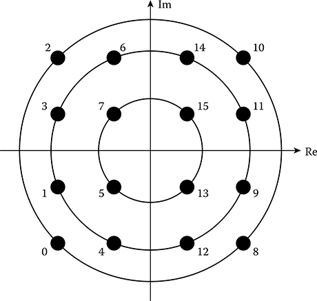
FIGURE 7.45 Generic square 16-QAM signal constellation.
For an average power of 5 dBm (3.16 mW), it can be computed that and from it: , and . In comparison with star 16-QAM, here the distances between the middle ring and the outer ring are much smaller. This means that to achieve the same BER, square 16-QAM needs a higher average power than star 16-QAM. The decision method for square 16-QAM is more complicated than that for Star 16-QAM. First, the decision between the three amplitude possibilities of each ring should be made; then, depending on the ring level, the decision is made between four or eight phase possibilities.
7.4.4.2 Offset-Square 16-QAM
To optimize the phase detection of the middle ring, it is envisaged that the phase differences between neighboring symbols on the middle ring in square 16-QAM should be equal. Thus, the shifted-square 16-QAM is introduced by shifting (rotation) symbols on the middle ring to obtain equal phase differences between all neighboring symbols as shown in Figure 7.7. After shifting the symbols on the middle ring, the distances between all direct neighbors are not necessarily equal. In comparison with square 16-QAM, this constellation may offer more robust detection against phase distortions according to our amplitude and phase detection method introduced in Section 7.4.7.
7.4.5 Detection Methods
In the case of differential encoding for the 16-QAM format, as described in Chapters 4 and 5, two different detection methods can be employed to demodulate and recover the data in the receiver: (1) direct detection and (2) coherent detection. Further details on the receivers will be given in Section 7.4.7.
In this section, direct detection means detection with Mach–Zehnder delay interferometric (MZDI) or (2 × 4) 90° hybrid, and coherent is similar except that a local oscillator (LO), a very narrow-linewidth laser, is used to mix the signal and its lightwaves to generate the IF or baseband signals with preservation of the modulated phase states. Each of these two receiving methods has different implementations, which can be introduced as follows.
7.4.5.1 Direct Detection
Unlike coherent detection, differential decoding is done for direct detection in the optical domain. Indeed, this is equivalent to self-homodyne coherent detection. This has the disadvantage of the transmitted absolute phase being lost after differential decoding. However, the relative phase (the phase of differential decoded signal) remains in the electrical domain, which makes electrical equalization still possible. The equalization with relative phases is more difficult, and the results can be worse than that with absolute phases. The advantage of direct detection, compared to coherent detection, is that the synchronization of a local laser with that of the signal lightwave is omitted. There are two methods to implement direct detection: one is with MZDI, and the other is with a (2 × 4) 90° hybrid coupler.
7.4.5.2 Coherent Detection
In a coherent receiver, an LO is used to mix its signal with the incoming signal lightwave for demodulation. As a result, the phase can be preserved in the electrical domain. This makes the electrical equalization very effective in coherent detectors. For coherent detectors, differential decoding is done in the electrical domain. On the basis of the intermediate frequency (fIF) defined as fIF = fs - fLO, three different coherent methods can be distinguished: (1) homodyne receiver, (2) heterodyne receiver, and (3) intradyne receiver. Only the homodyne receiver is included in this section, and the other two are only briefly mentioned.
7.4.5.2.1 Homodyne Receiver
A receiver is called homodyne when the carrier frequency (fs) and the LO frequency (fLO) are the same
In practice, because of the laser linewidth, a carrier synchronization must be implemented to set the center frequency and the phase of the LO to the same values as those in the incoming signal. For homodyne receivers, carrier synchronization can be implemented in the optical domain via an optical phase-locked loop (OPLL). Carrier synchronization failure causes degradation in the receiver’s performance, but in this chapter, this effect is not considered, and perfect synchronization in the receiver (a perfect single spectrum line) is assumed. Alternatively, as mentioned later, a heterodyne receiver using only one π/2 hybrid coupler with the associated electronic demodulation circuitry can be used to simplify the receiver configuration for coherent detection. Polarization control is another critical difficulty in all coherent receivers, which too is not included in this book. The implementation of homodyne receivers for the star 16-QAM is described in several textbooks.
7.4.5.2.2 Heterodyne Receiver
For this kind of receiver, the following applies
Bopt is the optical bandwidth of the transmitted signal. The IF will be mixed in the electrical domain with a synchronous or asynchronous method in the low-pass domain. In the case of synchronous demodulation, the phase synchronization can be done in the electrical domain. The implementation complexity of heterodyne receivers in the optical domain is less than that of homodyne receivers.
7.4.5.2.3 Intradyne Receiver
The intradyne receiver requires
The phase synchronization in the intradyne receiver can be done in the digital domain. That makes the intradyne receiver less complex in the optical domain than the homodyne receiver.
The intradyne receiver compared to the heterodyne receiver has the advantage that its processing bandwidth is smaller. The disadvantage of the intradyne receiver is that it has a higher laser line-width requirement than the heterodyne receiver.
7.4.6 Transmitter Design
There are many ways to implement the transmitter for star 16-QAM described in the previous section. For the simulations in this book, the parallel transmitter shown in Figure 7.46 is implemented. The bit stream enters the differential encoder module after serial-to-parallel conversion.
The differential encoder implements the following processes: (1) The four parallel bits that have arrived at the module are mapped (Gray coding) into symbols according to the gray coding for star 16-QAM mapping; (2) the precoded symbols are differentially encoded (differential coding); and (3) the differentially encoded symbols are mapped again to other symbols to drive the Mach– Zehnder modulators (MZMs) according to the star 16-QAM mapping of Table 7.5.
Each symbol at the output of the differential encoder module is represented by four bits. The bits are sent to pulse formers. The first two bits drive the first MZMs, with lightwaves generated from the CW laser. If the input bit is equal to 1, then the output of the MZM is −1, and in the other case the output of the MZM is a 1 (after sampling). After combining the output signals of these two MZMs and considering the 90° phase delay in one arm, we obtain the QPSK signal shown in Figure 7.46.
The third bit from the differential encoder output drives a PM to obtain the 8-PSK signal constellation from the QPSK signal [50, 51, 52, 53, 54, 55, 56 and 57]. If this bit is equal to 1, then the QPSK symbol will rotate by π/4. The 8-PSK signal constellation is shown in Figure 7.47. To achieve the two-level star 16-QAM signal constellation, another MZM is used to generate the second amplitude. If the fourth bit of the differential encoder output is 1, then this output symbol is set on the outer ring of the constellation, otherwise on the inner ring. This MZM sets the RR of the constellation. The signal constellation after MZM3 is shown in Figures 7.48 and 7.49.
The signal constellation in Figure 7.48 can be constructed from the whole constellation in Figure 7.43 with a rotation of π/6°. The advantage of this rotation is that on the real and imaginary axis of the constellation, only eight different amplitude levels instead of nine levels exist. So, another PM can be used between MZM3 and MZM-RZ to rotate the constellation by π/6°. This additional PM is not shown in Figure 7.46. To increase the receiver sensitivity and reduce the signal chirp, a RZ pulse carving with a duty cycle of 50% should be implemented at the end of the transmitter with an MZM driven by a sinus signal generator (SG). In our simulations, the MZMs in Figure 7.46 worked in push–pull operation, and the PMs were MZMs working as phase modulators.

FIGURE 7.46 Schematic diagram of the optical transmitter for Star 16-QAM.

FIGURE 7.47 Constellation of the first amplitude level generated from the optical transmitter for Star 16-QAM.

FIGURE 7.48 Constellation of the first and second amplitude levels generated from the optical transmitter for Star 16-QAM.
7.4.7 Receiver For 16-Star QAM
In this section, the implementation of a direct detection receiver and coherent receiver for star 16-QAM is explained. For coherent detection, there are many possibilities in the digital domain of the receiver to recover the data. The two methods implemented in this study detect the symbol before realizing differential decoding. The difference is that one detects the symbol directly using the method described in Section 7.4.2.1, while the other method employs a phase estimation algorithm, described in Section 7.4.2.2, before the symbol detection in order to cancel out the phase distortions (phase synchronization between the LO and the received signal). Another possibility, which is not implemented in this book, is to first do the differential decoding of the incoming signal and then the symbol detection.

FIGURE 7.49 Constellation of the first and second amplitude level at the receiver of Star 16-QAM after ten spans of dispersion-compensated standard SMF links.
7.4.7.1 Coherent Detection Receiver Without Phase Estimation
The structure of a coherent detection receiver is shown in Figure 7.50a. After transmission over fiber, the signal is amplified by an EDFA. The input power of the EDFA can be changed via an attenuator to set the OSNR. The output signal of the EDFA is sent to a bandpass (BP) filter in order to reduce the noise bandwidth.
An attenuator used to set the OSNR is required. The output signal of the EDFA is sent to a BP filter in order to reduce the noise bandwidth. The signal from the LO and the output of the BP filter are sent to a (2 × 4) π/2-hybrid and after it to two balanced detectors. The (2 × 4) 90°-hybrid and the balanced detectors demodulate and separate the received signal into in-phase (I) and quadrature (Q) components. The structure of the (2 × 4)π/2-hybrid coupler, the balanced detectors, and their mathematical description can be found in many published works on coherent optical communication technology. This coherent detector can be simplified further if heterodyne detection is used, as shown in Figure 7.50b, and is commercially available from Discovery Semiconductor [2].
Furthermore, an amplitude direct detection of in the electronic digital processor must be able to process the magnitude of the vector formed by I and Q components to determine the amplitude and phase of the received signals and hence their corresponding positions on the constellation and the decoding of the data symbols.
After LP filtering and sampling of the I and Q components, the samples are sent to the symbol detection and differential decoding module. The sampling is done in the center of the eye diagram. In the symbol detection and differential decoding module, we first recover the symbols from the incoming samples, then perform the differential decoding of symbols. In order to recover the symbols, the I and Q components are added together to a complex signal. Now, according to the original signal constellation, a decision must be made regarding to which symbol our complex sample must be mapped. This decision has two parts. First, an amplitude decision is made to determine to which ring the sample belongs. After this, a phase decision is made to determine to which of the eight possible symbols on a ring our sample belongs.

FIGURE 7.50 Coherent receiver for Star 16-QAM: (a) homodyne and heterodyne I and Q detection model and (b) heterodyne model with optical and electrical π/2 hybrid couplers-electrical detection of I and Q components.
For the amplitude decision, a known bit sequence for the receiver (training sequence) is used, and an amplitude threshold ath is defined according to
where s1(k) is the kth complex received samples of symbols on the inner ring, and n is the total number of symbols on the inner ring. s2(k) is the kth complex received sample of symbols on the outer ring and m is the total number of symbols on the outer ring. If the amplitude of one sample is larger than the threshold, the symbol is decided to be on the upper ring, otherwise on the inner ring. For the phase decision, the complex plane is divided into eight equiphase intervals. An index from 0 to 7 is assigned to this sample according to the interval the phase of the sample falls in. The next steps are differential decoding and mapping. The amplitude differential decoding and phase differential decoding are done separately. From their results, the symbol detection and after it the symbol-to-bit mapping is done in an inverse manner to that of the encoding in the transmitter.
Alternatively, the detection can be conducted with a heterodyne receiver that uses only a single π/2 hybrid optical coupler. It is then detected by the two photodiodes and coupled through a π/2 electrical hybrid coupler to detect the I and Q components for the phase and amplitude reconstruction of the received signals as shown in Figure 7.50b. The phase estimation can then be estimated by processing the I and Q signals in the electronic domain as described in the next section.
Owing to the two levels of Star 16-QAM, there must be an amplitude detection subsystem that can be implemented using a single photodetector followed by an electronic preamplifier as shown in later in the chapter in Figure 7.52. An electronic processor would be able to determine the position of the received signals on the constellation, and hence decoding can be implemented without any problem. The transmission performance presented here would not be affected. Only the technological implementation would be affected, and hence the electronic noise or optical noises’ contribution to the receiver can thus be taken into account.
7.4.7.2 Coherent Detection Receiver With Phase Estimation
The method and structure of this receiver is almost the same as for the previous receiver shown in Figure 7.50. The difference is that here a phase estimation is done before the phase decision in the symbol detection and differential decoding module. The dispersion of the single-mode optical fiber is purely phase effects and thus causes phase rotation, resulting in a phase decision error. The effect of dispersion on the Star 16-QAM format is shown in Figure 7.51.
The left plot (a) in the figure shows the sampled input signal into the fiber, and the plot on the right-hand side shows the sampled output of the fiber with a CD of 300 ps/nm. The fiber is considered to be linear in this simulation. A comparison of point A in both figures shows that this point is spread and rotated owing to dispersion. The spreading causes both phase and amplitude distortion, while the rotation causes only phase distortion. To solve the problem of phase rotation, the following phase estimation method is implemented. In general, this phase estimation method is for phase synchronization between the LO with the linewidth and signal to replace the OPLL.

FIGURE 7.51 Signal constellation (a) before and (b) propagation through the optical fiber link-phase rotation.
The incoming signal after sampling can be described as
where is the phase distortion due to the dispersion and noise, and ϕmod is the signal phase that must be recovered. Now, ϕtot must be eliminated from c(k). ϕmod values are π/8, 3π/8, 5π/8, π/8, 9π/8, 11π/8, 13π/8, and 15π/8. If these phase values are multiplied by 8, then
and from this
is the estimated phase for . In our simulations, arg(c8(k)) is filtered (the filter takes the average of 20 neighbor symbols) to avoid the phase jumps from symbol to symbol. The filter order of 20 is not optimized for each CD.
Now, the signal phase ϕmod(k) can be estimated as
After this phase estimation, the signal decision takes place by employing the same method as for the amplitude decision case.
7.4.7.3 Direct Detection Receiver
The block diagram of the direct detection receiver is shown in Figure 7.52. After the optical filter, the signal is split into two branches via a 3 dB coupler. We name these two branches the intensity branch and the phase branch. In the phase branch, the phase differential demodulation is done in the optical domain. The signal and the delayed signal at Ts (symbol duration) are sent into the (2 × 4) 90°-Hybrid and after that again into balanced detectors. At the output of the balanced detectors, the in-phase and quadrature components of the demodulated and differential decoded and received signal can be derived. After electrical filtering, the signal is sampled and then sent into the symbol detection module. In the amplitude branch, the amplitude is determined and differentially decoded. After the photodiode, the signal is low-pass-filtered and sampled and then fed into the amplitude detection and differential decoding module, a well-known optical coherent structure can be used to accomplish the amplitude decision and differential decoding. At the end, the in-phase and quadrature components and the amplitude branch are sent to the symbol detection module for further processes such as symbol detection and symbol-to-bit mapping.

FIGURE 7.52 Direct detection receiver for Star 16-QAM.
7.4.7.4 Coherent Receiver Without Phase Estimation
In this section, the required OSNR at 10−4 BER (using Monte Carlo simulation) is determined for the coherent and incoherent direct detection receivers. For each detection method, the optimum RR is obtained to minimize the OSNR at BER = 10−4 (the BER is determined via Monte Carlo simulations). After that, the DT at 2 dB OSNR penalty at BER = 10−4 is determined. The OSNR penalty is only 2 dB in our work and can have other values. The OSNR penalty is defined as the OSNR difference in decibels between the OSNR of the back-to-back case and the OSNR of other CD values. The DT is the CD interval that can be achieved with a certain OSNR penalty. In practice, the DT describes how much dispersion (residual dispersion) a system can tolerate with an OSNR penalty smaller than 2 dB. The simulations in this book are done with the simulation tool for both the linear and nonlinear channels. The simulation parameters are given in Table 7.6. The average input power of nonlinear fiber in our work is always 5 dBm.
7.4.7.4.1 Linear Channel
In Figure 7.53b, the optimum RR (RRopt) can be seen for each CD. RRopt is the RR that minimizes the OSNR for the given CD.
The optimum RR changes here nearly linear with CD and can be expressed as
RRopt increases with CD because an increase in CD means an increase in the phase rotation due to dispersion. This causes more phase detection errors and thus a higher OSNR requirement. An increase in the RR reduces the phase error probability but increases the amplitude error probability. RRopt is the best trade-off between phase errors and amplitude errors for each CD.
In the back-to-back case, RRopt is around 1.87. The theoretical value of RRopt is obtained as 1.77. The difference is because in the introduced coherent receiver, at first the symbol detection is done and then the differential decoding. In the case of differential decoding before symbol detection, the optimum RR is around 1.77 as excepted. To determine the RRopt for each CD, the RR is changed for each CD. The RR value that yields the smallest OSNR is RRopt. The RR step (it determines the RR accuracy) in simulations is 0.05. The characteristic for other CDs is similar to Figure 7.53a. To compare the OSNRs, the reference in this work is the OSNR from the back-to-back case. In the case of residual dispersion, it is of interest how the system performance changes with the change of RR. The simulation results of three different RRs can be seen in Figure 7.52.
TABLE 7.6
Simulation Parameters for 16-Star QAM.
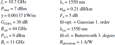
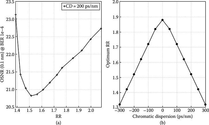
FIGURE 7.53 (a) OSNR versus RR (left) and (b) optimum RR versus CD (right) for coherent receiver without phase estimation.
As shown in Figure 7.52a, the OSNR performance for the back-to-back case is decreased if (in the simulated interval) the RR from 1.87 decreases. A degradation of 6.5 dB is determined if the RR decreases from 1.87 to 1.32. From the other side, the DT at 2 dB OSNR penalty increases (Figure 7.9b). The DT for RR = 1.87 is 220 ps/nm and for RR = 1.32 is 460 ps/nm. To understand the reason for this behavior, Figure 7.53a should be considered again. For each CD, if the RR decreases from the RRopt value, the OSNR increases rapidly. That means the RR value of 1.32 for the back-to-back case has increased the OSNR, but CD = 300 ps/nm has the minimum OSNR for this RR. The result is that the OSNR for the back-to-back case increases and decreases for the case without phase estimation in the linear channel. CD = 300 ps/nm. This effect causes a larger DT at a certain OSNR penalty. In a practical system, according to the higher requirement for the OSNR or DT, the RR can be chosen.
In Figure 7.54a (left), it can be seen as well that the required OSNR for |CD| = 300 ps/nm makes a jump compared to other CDs. With |CD| = 350 ps/nm, it is not possible to achieve a BER of 10−4. The reason is that |CD| = 350 ps/nm is the limit of the system. For this CD, it is not possible to transmit error free even without noise owing to phase rotations caused by dispersion (phase detection error). The signal constellation of the received signal after sampling with CD = 350 ps/nm can be seen in Figure 7.55; for example, some of the received symbols of A are over the phase threshold line, and they generate the detection errors.
A typical eye diagram at the output of the coherent receiver at the limit of the distortion is shown in Figure 7.56. Phase estimation can be implemented in the digital signal processor. Note that the signal constellation is rotated uniformly owing to the phase evolution of the spectral components of the modulated signals when propagating through the single-mode fiber as described in Chapter 2, and thus in the processing of the constellation. It is best if the reference frame of the phasor diagram is rotated to align with the constellation, which may simplify the phase estimation process at π/8 and its multiple values.
7.4.7.4.2 Nonlinear Effects
The optimum RR in the case of a nonlinear channel for different CDs is shown in Figure 7.57. As mentioned earlier, for linear channels, RRopt decreases with increase of CD too (Figure 7.58). The difference from Figure 7.53 is that the diagram is not symmetric. The reason for this is the interaction between the dispersion and the SPM. For a positive CD, the dispersion and the SPM have a constructive interaction, which results in a better OSNR performance. For a negative CD, the dispersion and the SPM have a destructive interaction that results in a much worse OSNR performance.

FIGURE 7.54 (a) OSNR versus CD and (b) OSNR penalty versus CD for coherent receiver.

FIGURE 7.55 Received signal constellation with CD = 350 ps/nm without noise for coherent receiver without phase estimation in linear channel.
This effect can be seen if Figure 7.53b (right) is compared with Figure 7.57 as shown in Figure 7.58. The curve slope for negative CD is higher in the nonlinear channel, which means the phase distortion is higher in the nonlinear channel. For positive CD, the slope in the nonlinear channel is lower, which means the phase distortion is less. The simulation results for different RRs are shown in Figure 7.59. Here again, it can be seen that the required OSNR for the back-to-back case increases with a decrease in the RR. Similarly, for the same reason as for the linear case, the DT at 2 dB OSNR penalty increases as well.
FIGURE 7.56 Typical eye diagram at the output of the coherent receiver under significant distortion limit of the 2A-8P Star 16-QAM.

FIGURE 7.57 RRopt versus CD in nonlinear channel for coherent receiver without phase estimation.

FIGURE 7.58 RRopt comparison in linear and nonlinear channels for coherent receiver without phase estimation.
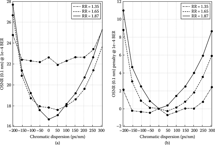
FIGURE 7.59 (a) OSNR versus CD and (b) OSNR penalty versus CD for coherent receiver without phase estimation in nonlinear channel. Note: No equalization, only phase estimation processing of I and Q received components in the electrical domain.
7.4.7.5 Remarks
The design of a Star 16-QAM modulation scheme is proposed for coherent detection for ultra-high-speed ultra-high-capacity optical fiber communications schemes. Two amplitude levels and eight phases (2A-8P 16-QAM) are considered to offer simple transmitter and receiver configurations and at the same time the best receiver sensitivity at the receiver. An optical SNR of about 22 dB is required for the transmission of Star 16-QAM over an optically amplified transmission dispersion-compensated link. A DT of 300 ps/nm is possible with a 1 dB penalty of the eye opening at 40 Gbps bit rate or 10 Giga-symbols/s with an OSNR of 18 dB. The OSNR could be about 22 dB for a 107 Gbps bit rate and a symbol rate of 26.75 G symbols/s. The transmission link consists of several spans of a total of 1000 km dispersion-compensated optically amplified transmission link. The optical gain of the in-line OAs is set to compensate for the attenuation of the transmission and compensating fibers with a noise figure of 3 dB.
The optical transmitter and receivers incorporating commercially available coherent receiver are structured and are sufficient for engineering the optical transmission terminal equipment for a bit rate of 107 Gbps and a symbol rate of 26.3 Gsymbol/s.
Furthermore, electronic equalization of the receiver PSK signals can be done using blind equalization, which would further improve the DT. For a symbol rate of 10.7 Gbps, this DT for a 1 dB penalty would reach 300 km of standard SMF. This electronic equalization can be implemented without any difficulty at 10.7 Gsymbol/s. For a 107 Gbps bit rate, a similar improvement of the DT can be obtained at 26.5 Gsymbol/s provided the electronic sampler can offer more than 50 GSamples/sec sampling rate.
7.4.8 Other Multilevel And Multi-Subcarrier Modulation Formats For 100 Gbps Ethernet Transmission
Numerous technologies have been introduced in recent years to cope with the ever-growing demand for transmission capacity in optical communications. Although the optical single-mode fiber offers enormous bandwidth in the order of magnitude of 10 THz, efficient exploitation of bandwidth started to become an issue a couple of years ago. Moreover, the limited speed of electronic and electro-optic devices such as modulators and photo receivers are considered a bottleneck for further increase of the data rate based on binary modulation.
For all these reasons, optical modulation formats offering a high ratio of bits per symbol are an essential technology for next-generation high-speed data transmission. In this way, data throughput can be increased while the required bandwidth in the optical domain as well as for electronic devices is kept at a lower level.
Because of the demand for transmission technologies offering high ratios of bits per symbol, two promising candidates to achieve a data rate of 100 Gbps per optical carrier are discussed, namely optical orthogonal frequency division multiplexing and 16-ary multilevel modulation. Their performance is analyzed by means of numerical simulation and by experiment.
7.4.8.1 Multilevel Modulation
Optical modulation formats incorporating four or eight bits per symbol were investigated in numerous contributions in the last couple of years (e.g., DQPSK [28] and 8-DPSK [29]). However, to carry out the step from 10 to 40 Gbps data rate using devices designed for 10 Gsymbol/s, the main challenge is to find the optimal combination of ASK and DPSK formats. Several approaches, which are reviewed in Ref. [30], are possible.
The simplest structure can be an extension of a 30 Gbps 8-DPSK by an additional PM resulting in 40 Gbps 16-DPSK. That is, in the complex plane, 16 symbols are placed onto a unit circle as shown in Figure 7.60a. Depending on the current bit at the data input of the additional PM, the 8-DPSK symbol is shifted by π/8 in case of a 1, while in case of a 0, the incoming phase of the symbol is preserved. Although it seems simple, experimental implementations have shown that the phase stability of the modulators and corresponding demodulators is very critical. Thus, the experimental setup must be stabilized. Moreover, 16-DPSK is suboptimal regarding exploitation of the full area that the complex plane offers. That is, the ratio of the symbol distance to signal power is low, resulting in poor receiver sensitivity.

FIGURE 7.60 Constellation of symbols in the complex plane for (a) 16-DPSK, (b) 16-ASK, (c) Star 16-QAM, and (d) 16ADPSK.
Similar behavior can be seen for the other extreme case of 16-ASK, as shown in Figure 7.60b. Here, the 16 symbols are placed on the positive real axis. The symbol distance is extremely narrow, resulting in poor sensitivity as well.
A much improved performance can be achieved by combining the amplitude and phase shift keying modulations of ASK and DPSK, the M-ary ADPSK as described earlier. There are a number of combinations of M-ary ADPSK. One approach can be the extension of a 8-DPSK by two rings of ASK levels. Thus, the 16 symbols appear as two rings in the complex plane with eight symbols per ring as shown in Figure 7.60c. Alternatively, this topology is known as Star-16 QAM. A second structure is given by combining DQPSK with four-level ASK (or equivalently, M-ary ADPSK), resulting in four rings with four symbols each as analyzed in earlier sections and shown in Figure 7.60d. Both structures effectively utilize the complex plane. However, both structures require that the sensitivity or the magnitude (diameters) of the rings have to be optimized to compromise the sensitivity performance of the DPSK and the ASK geometrical distribution. Especially, the inner ring has to be of a sufficient size to enable the different phases of the symbols on this ring to be distinguished. They are limited by the nonlinear effects of the transmission fiber and the noise contributed by the receiver and the in-line OAs. Hence, the distance between the constellations is limited by these two limits.

FIGURE 7.61 Measurement BER results for 16-ary inverse RZ-ADPSK modulation. Legend: b2b = back-to-back.
A strategy to mitigate this trade-off was introduced in Ref. 48 by using a special pulse shaping called inverted RZ. For binary ASK in conjunction with inverse RZ, a 0 is encoded as a temporary breakdown of the optical power, while for a 1 the optical power remains at a high level. Using this pulse shaping, for the M-ary ADPSK format, the four levels of the QASK part are transmitted by means of four different values for temporary decay of optical power. The DQPSK part, however, is transmitted by modulating the phase of the signal in the time slot in between, which implies that in the transmitter, the phase of the signal can be detected while the signal has maximum power.
Measurement results for this modulation format are depicted in Figure 7.61, where the BER is plotted as function of the OSNR measured within a 0.1 nm optical filter bandwidth. The main outcome is the fact that the DQPSK part is insignificantly disturbed by an additional QASK part. Moreover, even after transmission over 75 km of SSMF, the DPSK part shows a very low penalty. However, the QASK component inherently shows low performance due to the low symbol Euclidean distance. An improvement might be achieved by optimizing the duty cycle of inverse RZ and the RR. A simulated eye diagram of the 16-square QAM is shown in Figure 7.62 with the constellation before and after the optical transmission link of two optically amplified fiber spans with 2 km SSMF mismatch are shown in Figure 7.42.
7.4.8.2 Optical Orthogonal Frequency Division Multiplexing
Orthogonal frequency division multiplexing (OFDM) is a transmission technology that is primarily known from wireless communications and wired transmission over copper cables [31,32]. It is a special case of the widely known frequency division multiplexing (FDM) technique in which digital or analog data are modulated onto a certain number of carriers and transmitted in parallel over the same transmission medium. The main motivation for using FDM is the fact that due to parallel data transmission in the frequency domain, each channel occupies only a small frequency band. Signal distortions originating from frequency-selective transmission channels, the fiber CD, can be minimized. The special property of OFDM is its very high spectral efficiency. While for conventional FDM, the spectral efficiency is limited by the selectivity of the bandpass filters required for demodulation, OFDM is designed such that the different carriers are pairwise orthogonal. In this way, for the sampling point, the intercarrier interference (ICI) is suppressed, although the channels are allowed to overlap spectrally.

FIGURE 7.62 Eye diagram of 16-QAM detected at the output of a balanced receiver. Bit rate of 40 Gbps and baud rate of 10 Gbps.
Orthogonality is achieved by placing the different RF carriers onto a fixed frequency grid and assuming rectangular pulse shaping. It can be shown that in this special case, the OFDM signal can be described as the output of a discrete inverse Fourier transform with the parallel complex data symbols as input. This property has been one of the main driving aspects for OFDM in the past because modulation and demodulation of a large number of carriers can be realized by simple digital signal processing (DSP) instead of using many LOs in the transmitter and receiver. Recently, OFDM has become an attractive topic for digital optical communications [28, 29 and 30,33,34]. It is just another example of the current tendency in optical communications to consider technologies that are originally known from classical digital communications. Using OFDM appears to be very attractive because the low bandwidth occupied by a single OFDM channel increases the robustness toward fiber dispersion, allowing the transmission of high data rates of 40 Gbps and more over hundreds of kilometers without the need for dispersion compensation [35]. In the same way as for modulation formats such as DPSK or DQPSK that were introduced in recent years, in OFDM also the challenge for optical system engineers is to adapt a classical technology to the special properties of the optical channel and the requirements of optical transmitters and receivers.
Thus, two approaches have been reported recently. An intuitive approach introduced by Llorente et al. [29] makes use of the fact that the WDM technique itself already realizes data transmission over a certain number of different carriers. By means of special pulse shaping and carrier wavelength selection, the orthogonality between the different wavelength channels can be achieved, resulting in the so-called orthogonal WDM technique (OWDM). However, with this technique, the option of simple modulation and demodulation by means of the discrete Fourier transforms (DFT) cannot be utilized as this kind of DSP is not available in the optical domain.
An alternative popular method is the generation of an electrical OFDM signal by means of electrical signal processing followed by modulation onto a single optical carrier [30,33,34]. This approach is known as optical OFDM (oOFDM). Here, the modulation is a two-step process: first, the electrical OFDM in Ref. [58] signal already is a broadband bandpass signal, which is then modulated onto the optical carrier. Second, to increase data throughput, oOFDM can be combined with WDM resulting in multi-Tbps transmission system as shown in Figure 7.63. Nevertheless, oOFDM itself offers different options for implementation. An important issue is optical demodulation, which can be realized either by means of direct detection (DD) or coherent detection (CoD) using an LO. DD is preferable owing to its simplicity. However, for DD the optical intensity has to be modulated. Because the electrical OFDM signal is quasi-analog with a zero mean and a high peak-to-average ratio, the majority of the optical power has to be wasted for the optical carrier (i.e., an additional DC value of the complex baseband signal), resulting in low receiver sensitivity. For CD, in addition, the bandwidth efficiency is twice as high as for DD because for pure intensity modulation inherently a double-sideband signal is generated. For CD, a complex optical I–Q modulator composed of two real modulators in parallel followed by superposition with a π/2 phase shift allows for transmission of twice as much data within the same bandwidth. For intensity modulation, the bandwidth efficiency may be increased by suppressing one of the redundant sidebands, resulting in optical OFDM with single-sideband (SSB) transmission. First, the serial data can be converted to parallel streams. These parallel data sequences are then mapped to QAM constellation in the frequency domain, and then converted back by IFFT to the time domain. The time-domain signals are in the I and Q components, which are then fed into an I and Q optical modulator. This optical modulation can be DQPSK or any other multilevel modulation subsystem. At the end of the optical fiber transmission, the I and Q components are detected either by DD or CD. For CD, a (2 × 4) 90° hybrid coupler is used to mix the polarizations of the LO and that of the received signals. The outputs of the couplers are then fed into the balanced optical receivers. The mixing of the local laser source and that of the signals preserves the phase of the signals, which are then processed by a high-speed electronic processor. For direct detection, the I and Q components are detected differentially, and the amplitude and phase detection are then compared and processed similarly as for the coherent case.
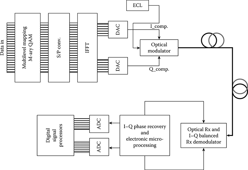
FIGURE 7.63 Schematic diagram of optical OFDM transmitter of a long-haul optical transmission system using multilevel modulation formats. ECL = external cavity laser.
In order to show the robustness of oOFDM toward fiber dispersion and also fiber nonlinearity, numerical simulations are carried out for a data stream at a 42.7 Gbps data rate. The number of OFDM channels can be varied between Nmin = 256 and Nmax = 2048. A guard interval of 12 ns can be inserted, a strategy belonging inherently to OFDM technology that ensures the orthogonality of the different channels in case of a transmission channel with memory. For the optical modulation, intensity modulation using a single MZM in conjunction with SSB filtering and direct detection was implemented. The nonlinear optical transmission channel consisted of eight 80 km non-DCF spans of SSMF. As a criterion for performance, the required OSNR for a BER of 10−3 (Monte Carlo) is measured. Using forward error correct (FEC), after decoding this is transferred into a BER below 10−9 depending on the specific code.
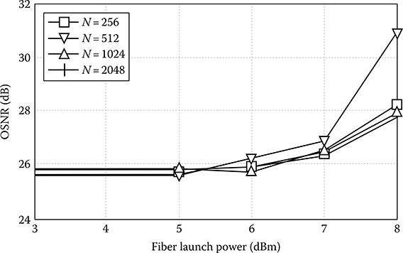
FIGURE 7.64 Simulation result for 42.7 Gbps OFDM transmission over 640 km of standard single-mode fiber; OSNR required for BER = 10−3 (Monte Carlo simulation) as function of fiber launch power.
Figure 7.64 shows the required OSNR as function of the fiber launch power for different values of N. The most important result is that transmission is possible over 640 km over SSMF without any dispersion compensation. This can be explained by the fact that even for the lowest value of Nmin = 256, each subchannel occupies a bandwidth of approximately 42.7 GHz/256 = 177 MHz, resulting in high robustness toward fiber dispersion.
The principal difficulties of optical OFDM are that the pure delay, owing to the variation of the refractive index of the fiber with respect to the optical frequency, leads to bunching of the subchannels and hence an increase of the optical power; thus, an unexpected SPM may occur in a random manner. Chapter 11 describes this OFDM modulation format.
7.4.8.3 100 Gbps 8-DPSK–2-ASK 16-Star QAM
7.4.8.3.1 Introduction
A multilevel modulation scheme enables the transmission baud rate to be reduced, thus obtaining spectral efficiency. Another significant advantage of this modulation scheme is the reduction of the requirement of high-speed processing electronics. This is of particular interest for high-speed optical transmission systems.
This part of the chapter investigates a multilevel modulation scheme that has eight phases and two amplitude levels. This scheme, which is called 8-DPSK–2-ASK, effectively utilizes four bits per symbol for transmission, in which is the first three bits are for coding phase information while the coding of the amplitude levels is implemented with the fourth bit. As a result, the transmission baud rate is equivalently a quarter of the bit rate from the bit pattern generator.
This section is organized as follows: Section 7.4.8.3.2 presents a detailed description of the optical transmitter for generating 8-DPSK–2-ASK signals. In Section 7.4.8.3.3, the detailed configuration of the receiver is provided. The configuration of the optical transmitter and receiver is based on that reported by Djordjevic and Vasic [36]. Section 7.4.8.3.4 describes a study on DT and the transmission performance of the 8-DPSK–2-ASK scheme. Finally, a short summary of the report is provided.
7.4.8.3.2 Configuration Of 8-DPSK–2-ASK Optical Transmitter
There have been several different configurations of an optical transmitter for generating multiphase/ level optical signals with the use of AMs or PMs arranged in either serial or parallel configurations [32,36, 37, 38 and 39]. However, the optical transmitters reported in Refs. [32,36, 37, 38 and 39] require a precoder with high complexity. However, the configuration reported by Ivan et al. [36] utilizes the Gray mapping technique to differentially encode the phase information, and this significantly reduces the complexity of the optical transmitter. In addition, as elaborated in more detail in Section 7.3, this pre-coding technique enables a detection scheme using the I–Q demodulation techniques, equivalent to those employed in coherent transmission systems.
The optical transmitter of the 8-DPSK–2-ASK scheme employs the I–Q modulation technique with two MZIMs in parallel and a π/2 optical PM, as shown in Figure 7.65. At each kth instance, the absolute phase of transmitted lightwaves θk is expressed as θk = θk−1 + Δθk, where θk−1 is the phase at (k − 1)th instance, and Δθk is the differentially coded phase information. The encoding of this Δθk for generating 8-DPSK–2-ASK modulated optical signals (four bits per transmitted symbol) follows the well-known Gray mapping rules. This Gray mapping phasor diagram is shown in Figure 7.66. The phasor is normalized with the maximum energy on each branch, that is, E1/2.
The amplitude levels are optimized so that the Euclidean distances d1,d2, and d3 are equal, that is, d1 = d2 = d3. After derivation, we obtain: r1 = 0.5664. The I and Q field vectors corresponding to the Gray mapping rules from the M-ADPSK precoder (see Figure 7.65) are provided in Table 7.7.
The foregoing transmitter configuration can be replaced with a dual-drive MZIM. The explanation and derivation for generating 8-DPSK–2-ASK optical signals are also based on the phasor diagram of Figure 7.66. In this case, the output field vector is the sum of two component field vectors, each of which is not only determined by the amplitude but also by initially biased phases [51, 52, 53, 54, 55 and 56].
7.4.8.3.3 Configuration Of 8-DPSK–2-ASK Detection Scheme
The detection of 8-DPSK–2-ASK optical signals is implemented with the use of two Mach–Zehnder delay interferometric (MZDI) = balanced receivers (see Figure 7.67).
Several key features of this detection structure are as follows:
The MZDI introduces a delay corresponding to the baud rate.
One arm of the MZDI has a π/4 optical phase shifter, while the other arm has an optical phase shift of −π/4.
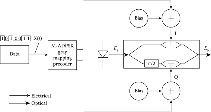
FIGURE 7.65 Optical transmitter configuration of the 8-DPSK–2-ASK modulation scheme.

FIGURE 7.66 Gray mapping for optimal 8-DPSK–2-ASK modulation scheme.
TABLE 7.7
I and Q Field Vectors in 8-DPSK–2-ASK Modulation Scheme Using Two MZIMS in Parallel
The outputs from two balanced receivers are superimposed positively and negatively, which leads to I and Q detected signals, respectively. The I and Q detected components are expressed as and .
The I–Q detected components are demodulated using the popular I–Q demodulator in the electrical domain. These detected signals are then sampled and represented as shown in the signal constellation.

FIGURE 7.67 Detection configuration for the 8-DPSK–2-ASK modulation scheme.
7.4.8.3.4 Transmission Performance of 100 Gbps 8-DPSK–2-ASK Scheme
Performance characteristics of the 8-DPSK–2-ASK scheme operating at 100 Gbps bit rate are studied in terms of receiver sensitivity, DT, and the feasibility for long-haul transmission. The BERs are the pre-FEC BERs, and the pre-FEC limit is conventionally referenced at 2e−3. In addition, the BERs are evaluated by the Monte Carlo method.
7.4.8.3.5 Power Spectrum
The power spectrum of 8-DPSK–2-ASK optical signals is shown in Figure 7.68. It can be observed that the main lobe spectral width is about 25 GHz, as the symbol baud rate of this modulation scheme is equal to a quarter of the bit rate from the bit pattern generator. The harmonics are not highly suppressed, thus requiring bandwidth of the optical filter to be necessarily large in order not to severely distort signals.
7.4.8.3.6 Receiver Sensitivity and DT
The receiver sensitivity is studied by connecting the optical transmitter of the 8-DPSK–2-ASK scheme directly to the receiver for a back-to-back setup (see Figure 7.69). On the contrary, the DT is studied by varying the length of SSMF from 0 to 5 km (|D| = 17 ps/(nm · km). The received power is varied by using an optical attenuator. The optical Gaussian filter has BT = 3 (B is approximately 75 GHz). Modeling of receiver noise sources includes shot noise, an equivalent noise current density of at the input of the trans impedance electrical amplifier, and a dark current of 10 nA for each of the two photodiodes in the balanced structure. A fifth-order Bessel electrical filter with a bandwidth of BT = 0.8 is used.
The numerical BER curves of the receiver sensitivity for cases of 0–5 km SSMF are shown in Figure 7.70. The receiver sensitivity of the 8-DPSK–2-ASK scheme is approximately −18.5 dBm at BER = 1e−4. The receiver sensitivity at BER = 1e−9 can be obtained by extrapolating the BER curve of the 0 km case. The power penalty versus residual dispersion results are then obtained and plotted in Figure 7.71. It is realized that the 2 dB penalty occurs for the residual dispersion of approximately 60 ps/nm, or, equivalently, to 3.5 km SSMF.
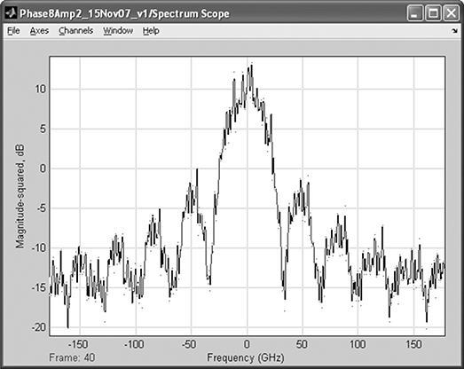
FIGURE 7.68 Power spectrum of 8-DPSK–2-ASK signals.
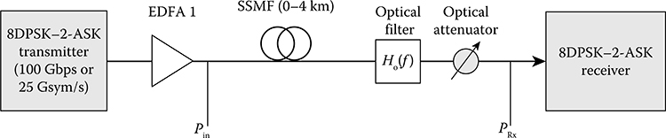
FIGURE 7.69 Setup for the study of receiver sensitivity (back-to-back) and dispersion tolerance (0–4 km SSMF) for the 8-DPSK–2-ASK modulation scheme.
7.4.8.3.7 Long-Haul Transmission
The long-haul transmission performance of this modulation format is conducted over ten optically amplified and fully compensated spans, and each span is composed of 100 km SSMF and 10 km DCF100 (Sumitomo fiber). As a result, the length of the transmission fiber link is 1100 km. This long-haul range is selected to reflect the distance between Melbourne and Sydney. The wavelength of interest is 1550 nm, and the dispersion at the end of the transmission link is fully compensated. The simulation setup is shown in Figure 7.69. In addition, the fiber attenuation due to SSMF and DCF is also fully compensated by using two EDFAs with optical gains as depicted in Figure 7.72. These EDFAs have a noise figure set at 5 dB.
Numerical transmission BERs are plotted against the received powers in Figure 7.73 and compared to the back-to-back BER curve. It can be observed that the BER curve of 1100 km follows a linear trend and feasibly reaches 1e−9 if extrapolated as shown in Figure 7.73. It should be noted that this transmission performance can be significantly improved with the use of a high-performance FEC scheme.

FIGURE 7.70 Receiver sensitivity (back-to-back) and dispersion tolerance (0–4 km SSMF) for the 8-DPSK– 2-ASK modulation scheme.

FIGURE 7.71 Power penalty due to residual dispersions for the 8-DPSK–2-ASK modulation scheme.

FIGURE 7.72 Transmission setup of 1100 km optically amplified and fully compensated fiber link.

FIGURE 7.73 BER versus receiver sensitivity for 8-DPSK–2-ASK modulation format transmission.
7.4.9 Concluding Remarks
The ever-increasing bandwidth hunger in telecommunication networks based mainly on optical fiber communication technology indicates that low bandwidth-efficient modulation formats such as ASK would no longer satisfy the transmission capacity demands, and new advanced optical modulation schemes should replace ASK in the near future. Advanced optical modulation schemes, especially the multilevel amplitude and phase schemes presented in this chapter, are able to (1) provide long reach, error-free, and high transmission capacity; (2) provide high bandwidth efficiency (no. bits/Hz parameter); (3) push the bit rate well above what could be offered by electronic technology, for example, 100 Gbps with the detection at the symbol rate; (4) tolerate dispersion and nonlinearity; and (5) to maximally utilize the existing optical network infrastructure.
Current developments of photonic technology have enabled the use of differential phase modulation and demodulation in the optical domain. Presently, the BDPSK and DQPSK formats have received great attention owing to their improvement in the receiver sensitivity as compared with ASK. Furthermore, the RZ and CSRZ formats would assist the battle against nonlinear effects. However, as long as transmission capacity and bandwidth efficiency are concerned, MADPSK modulation formats would offer a better performance in the trading off for its complexity in the receiver structures.
Alternatively, there are other multilevel modulation schemes that offer further improvement of the optical transmission performance [10].
7.4.9.1 Offset MADPSK Modulation
Binary DPSK and quaternary DPSK (DQPSK) are just special cases of a more general class of differential phase modulation formats that map data bits into the phase difference between neighboring symbols. This phase difference Δϕi can be described as
where θ is the initial phase, and M is the total number of phase levels. This class of formats is called offset DPSK (ODPSK) and denoted as θ-M-DPSK. Specifically, with θ = 0, M = 2 or M = 4, θ-MDPSK becomes 0–2-DPSK or 0–4-DPSK, the conventional binary DPSK and DQPSK mentioned earlier.
ODPSK has been used to transmit over satellite nonlinear channels because its phase transition is smooth and can avoid a 180° phase jump [40]. As the fiber medium also exhibits nonlinearity, this modulation format attracts our attention as a candidate, together with ASK, for creating a new multilevel modulation format, possibly termed Offset MADPSK.
7.4.9.2 MAMSK Modulation
Minimum shift keying (MSK) is a form of OQPSK with sinusoidal pulse weighting [41]. In MSK, data bits are first coded into bipolar signals ±1, which are then separated into VI(t) and VQ(t) streams consisting of even and odd bits, respectively. In the next stage, VI(t) and VQ(t) are used to modulate a carrier fc to create a MSK signal s(t), which can be presented as [41]
MSK is a well-known modulation format in wireless communications with efficient spectral characteristics owing to the high compactness of its main lobe as compared with DPSK, and high suppression of the side lobes [42]. These characteristics indicate that the MSK signal is highly dispersion tolerant. A combination of MSK and ASK into MAMSK modulation would even improve the transmission performance without increasing the complexity of the detection scheme [43].
Multilevel techniques for 100 Gbps are given; in particular, OFDM with multicarrier and multilevel amplitude modulation with orthogonality between adjacent channels are proved to be cost-effective and appropriate for current electronic technologies. Two interesting approaches to achieve data transmission of 40 Gbps and beyond (e.g., 100 Gbps Ethernet) based on low symbol rate are discussed. On the one hand, oOFDM can combine a large number of parallel data streams into one broadband data stream with high spectral efficiency. Simulation results are shown for different values of the number of parallel data streams in a nonlinear environment [58]. On the other hand, 16-ary modulation formats enable 40 Gbps transmission with 10 GSym/s (i.e., 100 Gbps with 25 GSymbols/s). For a special case, namely inverse RZ 16ADQPSK, measurement results are demonstrated.
7.4.9.3 Star QAM Coherent Detection
The last two sections of the chapter describe two optical transmission schemes using both coherent and incoherent transmission and detection techniques, the 2A-8P Star QAM and 8DPSK 2ASK 16-Star QAM for 100 Gbps or 25 GSymbols/s [44, 45, 46, 47, 48, 49 and 50].
First, the design of a Star 16-QAM modulation scheme is proposed for coherent detection for ultra-high-speed ultra-high-capacity optical fiber communications schemes. Two amplitude levels and eight phases (2A-8P 16-QAM) are considered to offer significant simple transmitter and receiver configurations and at the same time the best receiver sensitivity at the receiver. An optical SNR of about 22 dB is required for the transmission of Star 16-QAM over an optically amplified transmission dispersion-compensated link. A DT of 300 ps/nm is possible with a 1 dB penalty of the eye opening at 40 Gbps bit rate or 10 Giga-symbols/s with an OSNR of 18 dB. The OSNR could be about 22 dB for a 107 Gbps bit rate and a symbol rate of 26.75 G symbols/s. The transmission link consists of several spans of total 1000 km dispersion-compensated optically amplified transmission link. The optical gain of the in-line OAs are set to compensate for the attenuation of the transmission and compensating fibers with a noise figure of 3 dB. The optical transmitter and receivers incorporating commercially available coherent receivers are structured and are sufficient for engineering of the optical transmission terminal equipment for a bit rate of 107 Gbps and a symbol rate of 26.3 GBaud/s.
Furthermore, electronic equalization of the receiver phase shift keying signals can be done using blind equalization, which would improve the DT much further. For a symbol rate of 10.7 Gbps, this DT for a 1 dB penalty would reach 300 km of standard SMF. This electronic equalization can be implemented without any difficulty at 10.7 GBaud/s. For a 107 Gbps bit rate, a similar improvement in the DT can be at 26.5 GBaud/s provided that the electronic sampler can offer a >50 Gig sampling rate.
Second, the transmitter and receiver configurations for generating 8-DPSK–2-ASK optical signals and direct detection are described as well as the transmission performance. In addition, the performance characteristics of this modulation format at 100 Gbps (equivalently, 25 GBaud/s) has also been investigated in terms of the receiver sensitivity, DT, and the long-haul transmission performance. The simulation results show that 8-DPSK–2-ASK is a promising modulation for very high-speed (100 Gbps) and long-haul optical communications.
Furthermore, another multidimension system using multiple carriers such as the OFDM scheme is introduced, and more details will be given in Chapter 11.
References
1. R. A. Linke and A. H. Gnauck, High-capacity coherent lightwave systems, IEEE J. Lightwave Technol., Vol. 6, No. 11, pp. 1750–1769, 1988.
2. L. N. Binh, Monash Optical Communication System Simulator. Part I: Ultra-long Ultra-High Speed Optical Fiber Communication Systems, Manual for Technical Development, Melbourne, Australia: ECSE Monash University, 2004.
3. G. Proakis, Digital Communication, New York: McGraw-Hill, 2001.
4. L. N. Binh and B. Laville, Simulink Models for Advanced Optical Communications: Part IV-DQPSK Modulation Format, Technical Report, Melbourne, Australia: ECSE Monash University, 2005.
5. A. H. Gnauck, X. Liu, X. Wei, D. M. Gill, and E. C. Burrows, Comparison of modulation formats for 42.7Gbs single-channel transmission through 1980 km of SSMF, IEEE Photon. Technol. Lett., Vol. 16, No. 3, pp. 909–911, 2004.
6. K. Sekine, N. Kikuchi, S. Sasaki, and S. Hayase, 40 Gb/s 16-ary (4 bit/symbol) optical modulation/ demodulation scheme, IEEE Electron. Lett., Vol. 41, No. 7, pp. 430–432, 2005.
7. T. Mizuochi, K. Ishida, T. Kobayashi, J. Abe, K. Kinjo, K. Motoshima, and K. Kasahara, A comparative study of DPSK and ASK WDM transmission over transoceanic distances and their performance degradations due to nonlinear phase noise, IEEE J. Lightwave Technol., Vol. 21, No. 9, pp. 1933–1943, 2003.
8. T. Hoshida, O. Vassilieva, K. Yamada, S. Choudhary, R. Pecqueur, and H. Kuwahara, Optimal 40 Gb/s modulation formats for spectrally efficient long-haul DWDM systems, IEEE J. Lightwave Technol., Vol. 20, No. 12, pp. 1989–1996, 2002.
9. S. Hayase, N. Kikuchi, K. Sekein, and S. Sasaki, Proposal of 8-state per symbol (binary ASK and QPSK) 30-Gb/optical modulation demodulation scheme, in Proceedings of European Conference on Optical Communication, paper Th2.6.4, ECOC 2003, Rimini, Italy, pp. 1008–1009, September 2003.
10. S. Walklin and J. Conradi, Multilevel signaling for increasing the reach of 10 Gb/s lightwave systems, IEEE J. Lightwave Technol., Vol. 17, No. 11, pp. 2235–2248, 1999.
11. Y. Miyamoto, A. Hirano, K. Yonenaga, A. Sano, H. Toba, K. Murata, and O. Mitomi, 320 Gb/s (8 × 40 Gb/s) WDM transmission over 367-km zero-dispersion-flattened line with 120-km repeater spacing using carrier-suppressed return-to-zero pulse format, IEEE Electron. Lett., Vol. 35, No. 23, pp. 2041–2042, 1999.
12. L. N. Binh, H. S. Tiong, T. L. Huynh, and D. D. Tran, DPSK RZ modulation formats generated from dual drive interferometric optical modulators. Unpublished works.
13. L. N. Binh and Y. L. Cheung, DWDM Advanced Optical Communication–Simulink Models: Part I– Optical Spectra, Technical Report, Melbourne, Australia: ECSE Monash University, 2005.
14. R. Hui, S. Zhang, B. Zhu, R. Huang, C. Allen, and D. Demarest, Advanced Optical Modulation Formats and their Comparison in Fiber-Optic Systems, Technical Report, Information and Telecommunication Technology Center, University of Kansas, 2004.
15. D. S. Lee, S. K. Daejeon, M. S. Lee, Y. J. Wen, and A. Nirmalathas, Electrically band-limited CSRZ-DPSK signal with a simple transmitter configuration and reduced linear crosstalk in high spectral efficiency DWDM systems, IEEE Photon. Technol. Lett., Vol. 16, No. 9, pp. 2135–2137, 2004.
16. C. Wree, RZ-DQPSK Format with High Spectral Efficiency and High Robustness Towards Fiber Nonlinearities, University of Kiel, 2002.
17. T. L. Huynh, L. N. Binh, D. D. Tran, and Q. H. Lam, Long-haul ASK and DPSK optical fiber transmission systems: Simulink modeling and experimental demonstration test beds, in Proceedings of IEEE Tencon’05, Melbourne, Australia, November 2005.
18. H. Kim and P. J. Winzer, Robustness to laser frequency offset in direct detection DPSK and DQPSK systems, IEEE J. Lightwave Technol., Vol. 21, No. 9, pp. 1887–1891, 2003.
19. R. A. Griffin et al., 10 Gb/s optical differential quadrature phase shift key (DQPSK) transmission using GaAs/ AlGaAs integration, in Proceedings of OFC 2002, postdeadline paper FD6, Anaheim, CA, USA, 2002.
20. N. Yoshikane and I. Morita, 1.14 b/s/Hz spectrally-efficient 50x85.4 Gb/s transmission over 300 km using co-polarized CS-RZ DQPSK signals, in Proceedings of OFC 2004, postdeadline paper PDP38, Los Angeles, CA, 2004.
21. D. D. Tran, L. N. Binh, T. L. Huynh, and H. S. Tiong, Geometrical and phasor representation of multilevel amplitude-phase modulation formats and photonic transmitter structures, in Proceedings of the IEEE Tencon’05, Melbourne, Australia, November 2005.
22. G. P. Agrawal, Fiber-Optic Communication Systems, New York: Wiley, 1992.
23. K.P. Ho, Generation of arbitrary quadrature signals using one dual-drive modulator, IEEE J. Lightwave Technol., Vol. 23, No. 2, pp. 764–770, 2005.
24. G. P. Agrawal, Nonlinear Fiber Optics, 2nd ed., Boston, MA: Academic Press, 1995.
25. T. V. Muoi, Stepped-index optical fiber systems, Ph.D. Thesis, University of Western of Australia, 1978.
26. L. N. Binh et al., Monash Optical Communication System Simulator. Wavelength Division Multiplexed Optical Communication Systems and Networks, Manual for Technical Development, Melbourne, Australia: Monash University, 1997.
27. A. Gumaste and T. Antony, DWDM Network Designs and Engineering Solutions, Cisco Press, Milton Keynes, UK, 2002.
28. S. L. Jansen, I. Morita, N. Takeda, and H. Tanaka, 20-Gb/s OFDM transmission over 4160-km SSMF enabled by RF-pilot tone phase noise compensation, in Proceedings of OFC 2007, paper PDP15, Anaheim, CA, USA, March 2007.
29. R. Llorente, J. H. Lee, R. Clavero, M. Ibsen, and J. Martí, Orthogonal wavelength-division-multiplexing technique feasibility evaluation, J. Lightwave Technol., Vol. 23, pp. 1145–1151, 2005.
30. A. J. Lowery, L. Du, and J. Armstrong, Orthogonal frequency division multiplexing for adaptive dispersion compensation in long haul WDM systems, in Proceedings of OFC 2006, paper PDP39, Anaheim, CA, USA, March 2006.
31. J. Leibrich, A. Ali, and W. Rosenkranz, Optical OFDM as a promising technique for bandwidth- efficient high-speed data transmission over optical fiber, in Proceedings of the 12th International OFDM-Workshop 2007, InOWo 2007, 29, 30, August 2007, Hamburg, Germany.
32. H. Yoon, D. Lee, and N. Park, Performance comparison of optical 8-ary differential phase-shift keying systems with different electrical decision schemes, Opt. Express, Vol. 13, No. 2, pp. 371–376, 2005.
33. L. Hanzo, M. Münster, B. J. Choi, and T. Keller, OFDM and MC-CDMA for Broadband Multi-User Communications, WLANs and Broadcasting, New York: Wiley, 2003.
34. W. Shieh and C. Athaudage, Coherent optical orthogonal frequency division multiplexing, Electron. Lett., Vol. 42, pp. 587–589, 2006.
35. L. N. Binh, Monash Optical Communication System Simulator. Part II: Ultra-long Ultra-High Speed Optical Fiber Communication Systems, Manual for Technical Development, Melbourne, Australia: ECSE Monash University, 2004.
36. I. B. Djordjevic and B. Vasic, Multilevel coding in M-ary DPSK/differential QAM high-speed optical transmission with direct detection, IEEE J. Lightwave Technol., Vol. 24, pp. 420–428, 2006.
37. M. Serbay, C. Wree, and W. Rosenkranz, Implementation of different precoder for high-speed optical DQPSK transmission, Electron. Lett., Vol. 40, No. 20, pp. 1–2, 2004.
38. M. Serbay, C. Wree, and W. Rosenkranz, Experimental investigation of RZ-8DPSK at 3 × 10.7 Gb/s, in Proceedings of LEOS 2005, paper WE3, Sydney, Australia, October 2005.
39. M. Seimetz, M. Noelle, and E. Patzak, Optical systems with high-order DPSK and star QAM modulation based on interferometric direct detection, IEEE J. Lightwave Technol., Vol. 25, pp. 1515–1530, 2007.
40. C. Wree et al., Offset-DQPSK modulation format for 40 Gb/s and comparison to RZ-DQPSK in WDM environment, in Proceedings of OFC 2004, paper MF62, Los Angeles, CA, USA, February 2004.
41. S. Pasupathy, Minimum shift keying: A spectrally efficient modulation, IEEE Commun. Mag., Vol. 17, pp. 14–22, 1979.
42. T. Sakamoto et al., Optical minimum-shift keying with external modulation scheme, Opt. Express, Vol. 13, pp. 7741–7747, 2005.
43. M. Ohm and J. Speidel, Quaternary optical ASK-DPSK and receivers with direct detection, IEEE Photon. Technol. Lett., Vol. 15, No. 1, pp. 159–161, 2003.
44. O. Boyraz, T. Indukuri, and B. Jalali, Self-phase modulation induced spectral broadening in silicon waveguides, in Proceedings of CLEO2004, Vol. 2, paper CThj2, May 2004.
45. G. Goeger, M. Wrage, and W. Fischler, Cross-phase modulation in multispan WDM systems with arbitrary modulation formats, IEEE Photon. Technol. Lett., Vol. 16, No. 8, pp. 1858–1860, 2004.
46. G. Turin, An introduction to matched filters, IEEE Trans. Information Theory., Vol. 6, No. 3, pp. 311–329, 1960.
47. B. Zhu, 3.08 Tbit/s (77x42.7 Gb/s) WDM transmission over 1200 km fiber with 100 km repeater spacing using dual C- and L-band hybrid Raman/erbium-doped inline amplifiers, IEEE Electron. Lett., Vol. 37, No. 13, p. 844, 2001.
48. H. Rongqing, Z. Benyuan, H. Renxiang, T. A. Christopher, R. D. Kenneth, and D. Richards, Subcarrier multiplexing for high-speed optical transmission, IEEE J. Lightwave Technol., Vol. 20, No. 3, pp. 417–427, 2005.
49. A. H. Gnauck, and P. J. Winzer, Optical phase-shift-keyed transmission, IEEE J. Lightwave Technol., Vol. 23, No. 1, pp. 115–130, 2005.
50. K.P. Ho, Error probability of DPSK signals with cross-phase modulation induced nonlinear phase noise, IEEE J. Sel. Top. Quant. Electron., Vol. 10, No. 2, pp. 421–427, 2004.
51. G. P. Agrawal, Self-phase modulation and spectral broadening of optical pulses in semiconductor laser amplifiers, IEEE J. Quant. Electron., Vol. 25, No. 11, pp. 2297–2306, 1989.
52. J. P. Gordon and L. F. Mollenauer, Phase noise in photonic communications systems using linear amplifiers, Opt. Lett., Vol. 15, No. 23, pp. 1351–1353, 1990.
53. C. Michel, Techniques for estimating the bit error rate in the simulation of digital communication systems, IEEE J. Sel. Areas Commun., Vol. SAC-2, No. 1, pp. 153–170, 1984.
54. H. Kim and A. H. Gnauck, Experimental investigation of the performance limitation of DPSK systems due to nonlinear phase noise, IEEE J. Lightwave Technol., Vol. 15, No. 2, pp. 320–322, 2005.
55. C. Wree, J. Leibrich, and W. Rosenkranz, RZ-DQPSK format with high spectral efficiency and high robustness towards fiber nonlinearities, in Proceedings of ECOC 2002, paper 9.6.6, Copenhagen, Denmark, September 2002.
56. N. Kikuchi, Amplitude and phase modulated 8-ary and 16-ary multilevel signaling technologies for high-speed optical fiber communication, in Proceedings of APOC 2005, paper 602127, Shanghai, China, October 2005.
57. M. Serbay, T. Tokle, P. Jeppesen, and W. Rosenkranz, 42.8 Gbit/s, 4 bits per symbol 16-ary inverse-RZ-QASK-DQPSK transmission experiment without polmux, in Proceedings of OFC 2007, paper OThL2, Anaheim, CA, USA, March 2007.
58. A. Ali, Investigation of OFDM-transmission for direct optical systems, Dr. Ing. Dissertation, Lehrstuhl für Nachrichten- und Übertragungstechnik, Christian ALbrechts Unviversitaet zu Kiel, Germany, 2012.