
17
Temporal Lens and Adaptive Electronic/Photonic Equalization
The duality between the paraxial diffraction of beams in spatial domain and the dispersion of ultra-short pulses in time domain offer significant insights into pulse dynamics when propagating through single-mode optical fibers. A quadratic phase modulation in time (time lens) is the analog of a thin lens in space. Furthermore, an analogy between spatial and temporal imaging can be used to obtain the distortion-less expansion or compression of optical pulse sequences. Temporal imaging systems function toward focusing and defocusing the ultra-short pulses after propagating through a length of single-mode optical fiber. A quadratic phase modulator acts as a time lens via the quadratic phase modulation. Ultra-fast photonic signal processing in optical communication has emerged recently for long-haul optical transmission, and temporal imaging is expected to play a key role in the near future in this emerging technology. The significant application of temporal imaging is the adaptive equalization or, effectively, the refocusing of the broadened pulses by feeding them through an optical modulator that changes the phase of the carriers of the pulses to the opposite of the quadratic phase effects. This type of adaptive equalizer could eliminate any quadratic phase distortion, which normally can be compensated using passive devices such as dispersion-compensating fibers (DCFs), polarization-mode dispersion (PMD) compensator, and eliminators for timing jitter effects.
In this chapter, we demonstrate the propagation and equalization of a single pulse and a sequence of pulses through standard single-mode fiber (SMF). The system transmission performance with and without equalization at 160 Gbps bit rate is given in Figure 17.1. Analytical and simulation results show strong agreement in the effectiveness of this dispersion equalization technique. The 160 Gbps ultra-high-speed transmission system is very sensitive to both higher-order and time-varying dispersions, and it is proven that the equalization has improved the dispersion effects such as the group velocity dispersion (GVD), timing jitter. and polarization-mode dispersion (PMD). Pulse propagation and its equalization are investigated with 120 km SSMF transmission length. Simulation results have shown significant improvement in the bit error rate (BER) under the cases of with and without the equalization.
17.1 Introduction
When an optical pulse propagates through an SMF, its optical spectrum would travel down the fiber at different speeds, due to material and waveguide dispersion as well as polarization modal delay, and naturally the nonlinear phase effects if the intensity of the pulse is above the SPM threshold level. In case the bit rate reaches 160 Gbps, the compensation and equalization is preferred to be in an active mode, and thus an optical phase modulator operating at a very high speed should be used. An integrated optical phase modulator could change the phase (controlled shift on the phase of a light beam) of the optical signal by applying a driving traveling wave voltage V. When the electric field is generated and applied across an optical channel waveguide formed on an electro-optic substrate, the change in the refractive index would induce a change in the propagation constant of the propagating mode and create a phase shift for all traveling lights through that region [1]. Figure 17.1 shows a phase shift at the output of the phase modulator. This type of equalization can be implemented adaptively.
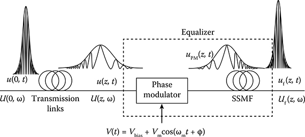
FIGURE 17.1 A schematic of the optical system communication incorporating an equalizer with sinusoidal driving voltage, 40 GHz clock recovered signals for phase modulation.
Furthermore, it is much more difficult to fully compensate a higher-order dispersion of the third or fourth order in ultra-fast signal processing by using only DCF. Mismatched compensation between SMF and DCF would be accumulated over long distances, causing serious distortion of the received pulses. Therefore, another dispersion compensation scheme that can be implemented at the front end of the receiver in order to fully recover the transmitted signals is reported in this chapter.
Currently, the remarkable progress of integrated photonic technology makes possible the fabrication of active devices such as modulators, integrated transmitters, and so on, which are commercially available for operating speeds of up to several GHz. In particular, ultra-wideband optical phase modulators can offer significant phase modulation over a very short period, thus enabling the alteration of the phase of the lightwave carrier embedded within a very narrow-width pulse sequence. These modulators thus enable the possibility of chirping the carrier frequency, and hence introduce dispersion in the negative or positive sense for equalization of the phase disturbance within an optical pulse due to the quadratic phase effects of single-mode optical fibers. The phase modulation for equalization can be implemented in an adaptive mode.
The propagation of an optical pulse through an optical fiber can be considered as the evolution of a pulse through a quadratic phase medium, that is, the amplitude remains invariant, but its phase, the carrier phase, is altered following a quadratic function of its spectral components. This phenomenon is indeed similar to the diffraction of a lightwave beam through a spatial slit. Alternatively, one could consider the fiber as a temporal lens that defocuses or focuses the guided lightwave beam, depending on the sign of the dispersion factor of the fiber. Therefore, there is duality between the spatial and temporal domains of the propagation of lightwave beams or pulse sequence through a spatial lens or a guided wave optical device. The correction of the blurred optical pulses can be made via the modulation of the phase of the carrier within the pulse period, whether in passive or active and adaptive modes. We demonstrate that equalization can be achieved by using an optical phase modulator, and the performance of this online adaptive equalization is very effective for ultra-high-speed optical transmission systems, especially at 160 Gbps.
The organization of this chapter is as follows. In Section 17.2, space–time duality and its applications as well as principles of temporal imaging are described. The temporal imaging, which is necessary and plays a key role in long-haul-transmission optic fiber, is also discussed. Section 17.3 presents simulation results of the equalization of the impairment due to second-order and third-order dispersion (TOD) of an SMF. Advantages and disadvantages of using sinusoidal and ideal parabolic driving voltage on an optical phase modulator for equalization are also given in detail. Section 17.4 discusses the simulation model by MATLAB® and Simulink® for the transmission, modulation, and equalization techniques of a 160 Gbps transmission system. Section 17.5 outlines the significant results of a single-pulse transmission and equalization of the 160 Gbps transmission system. BER characteristics and eye diagrams are illustrated, together with the transmission performance. Finally, some concluding remarks are stated in Section 17.6.
17.2 Space–Time Duality and Equalization
The duality between the spatial domain and time domain has been investigated, leading to the formation of temporal imaging, and thus the analogy of a thin lens in spatial domain and a quadratic phase modulation in time domain [2]. Temporal imaging is a technique that enables the expansion or compression of signals in time, and their envelope profiles could be maintained in long-haul transmission [3,4]. Basically, the principle of temporal imaging is based on broadening pulse width due to fiber’s dispersion factor and the spreading of a beam due to Fresnel diffraction under far-field consideration. When optical signals propagating through a single-mode optical fiber are transmitted in the air, the pulse width of these signals are broadened due to the optical dispersion or diffraction effects. Consequently, the carrier frequencies of these signals would be chirped up or chirped down, depending on the transmission medium. Thus, the spectra of these waveforms would be broadened or compressed due to the changes in the phase of each frequency component. The Fresnel or Fraunhofer (far-field) diffraction was discussed by Papoulis in the 1960s [5], and signal dispersion is described by Agrawal [6,7]. We can also further clarify in this section.
Furthermore, a key element in a temporal imaging system is a time lens, which is considered a quadratic phase modulation in the time domain. In addition, a dispersive element, such as SSMF, DCF, or fiber Bragg grating (FBG), also performs an equivalent role of diffraction. A quadratic phase modulation could be produced by using several methods, and one of those that is popular for ultra-short-pulse compression or generation is an ultra-high-speed electro-optic phase modulator [8,9]. Assuming that chirped signals are launched into a divergent or convergent lens in the spatial domain or a quadratic phase modulator in the time domain time which would chirp the frequencies of the embedded lightwave carriers in the modulated signal envelope. Each frequency component of a linear chirped pulse generated by a parabolic phase modulator travels at a different speed, due to the GVD in the fiber, and hence the media act as a time lens. Consequently, the frequency components of these signals are reorganized before they are again launched into free air or a dispersive element such as optical fiber. By using a suitable length or dispersion, both before and after a space lens or a time lens, the output pulses could be recovered or even shortened, as compared to the original pulses.
The main purpose of this chapter is to study space–time duality, and how to apply this property to design an adaptive equalization system for ultra-fast optical signal processing and equalization of distorted pulse sequences over an ultra-long-haul and ultra-high-speed optical fiber transmission system. The duality between spatial domain and time domain is proven and summarized. Furthermore, the broadening of a Gaussian pulse in transmission fiber is strongly influenced by the frequency chirping of the modulated carrier.
The duality between light diffraction in spatial domain and narrow-band dispersion in time domain has been studied recently. This duality could be used and applied to expand or compress transmitted pulses in time domain while those pulses’ shapes are maintained. This process can be termed as temporal imaging. The theory of temporal imaging is based on the duality between paraxial diffraction and narrow-band dispersion. This interesting duality is analyzed and discussed in more detail in Section 17.2.1.1 below. This section gives a review of the analogy between par-axial diffraction of a light beam in spatial domain and the temporal dispersion of a narrow-band pulse in a dielectric medium [2,10,11]. Furthermore, the space–time duality has also led to the employment of quadratic phase modulation devices such as optical adaptive equalizers [12] or electro-optic phase modulators [8] in the time domain, in the analogy of a thin lens in the spatial domain [13], which is equivalent to the phase modulation of the carrier frequency under the pulse envelope in the time domain. In addition, a real-time Fourier transformation that uses a time lens would be considered a temporal equivalence with the spatial Fourier transformation [14]. This equivalence can be used for the implementation of an equalization system, which is introduced in the next section.
17.2.1 Space–Time Duality
It is assumed throughout this chapter that the frequency spectrum of the carrier wave is monochromatic. We can then write the evolution of the carriers in the propagation equations without including the frequency term. This section describes the para-axial diffraction and the wave equation representing its dynamic behavior. We then obtain the essential equations for the spatial lens and the time lens for further propagations in an optical link.
17.2.1.1 Paraxial Diffraction
Maxwell’s equations would be used to obtain a 3D vector equation. The paraxial form of the Helmholtz equation and its solution are given as follows
and
The propagation direction is in the z-direction and polarization in the transverse plane of x- and y-axes. Owing to the paraxial approximation, the curvature of the field envelope in the direction or propagation (z-direction) is much less than the curvature of the transverse profile.
Therefore, it could be concluded that the term is much smaller compared to the terms , and , and therefore it might be eliminated. Finally, the electric field propagating down the z-axis can be found as
These equations are in parabolic form and similar to the heat diffusion equation. Therefore, the behavior of diffraction and dispersion, which is spreading like a temperature distribution, can be derived by using the solutions of the diffusion problem [2].
17.2.1.2 Governing Nonlinear Schrödinger Equation
An optical signal whose temporal envelope in the z-direction E(z, t) = u(z, t)ejωt propagating through an optical fiber can be represented by the nonlinear Schrödinger equation (NLSE)
where the amplitude u = u(z,t) is the complex envelope carried by the lightwaves of wavelength λ, along the propagation in z-axis, and t is the time variable. Pulse broadening is a result of the frequency dependence of β. By using Taylor series to expand β(ω) around the carrier frequency ωc, so that the second, third, and higher-order dispersion can be obtained as , β = −Dλ2/2πc is the GVD coefficient and the TOD factor, and related to the dispersion slope S. γ = n2ω/cAeff is the nonlinear coefficient of an optical fiber with an effective area of Aeff, corresponding to a mode spot size r0, where n2 is the nonlinear refractive index taking a typical value for silica-based glass of 2.6e−20 m2/w. If the losses during transmissions in the optical fiber can be ignored, and a value of β3 (i.e., about 0.117 ps3/km) is very small compared to a value of β2 (about 21.6 ps2/km), Equation 17.5 can thus be rewritten in normalized form as
17.2.1.3 Diffractive and Dispersive Phases
Different forms of diffusion could be modeled quantitatively using the diffusion equation, which go by different names, depending on the physical situation. Steady-state thermal diffusion is governed by Fourier’s law. In all cases of diffusion, the net flux of the transported quantity (atoms, energy, or electrons) equaled a physical property (diffusivity, thermal conductivity, electrical conductivity) multiplied by a gradient (a concentration, thermal, electric field gradient) [2].
The governing equations of the paraxial equation and the nonlinear Schrödinger equation follow the forms
and the equation of heat diffusion for 2D diffusion is
Paraxial, NLSE, and heat diffusion equations are thus governed by the same parabolic differential equation, and thus they should have similar forms. Let kx be the Fourier domain variable or the propagation constant in the x direction, and U(kx, ky,0) be the initial Fourier spectrum. By applying the 2D equation of heat diffusion to the two wave equations, solutions for 2D diffraction and wave propagation can be found [2].
Comparing Equations 17.9 and 17.10, it becomes clear that the envelope of the input pulse is similar to the paraxial diffraction. The terms (kx,ky) and x in spatial domain correspond to the terms ω and t in time domain, respectively. In other words, a beam displacement in the spatial domain corresponds to a pulse delay in the time domain [15]. According to Equations 17.9 and 17.10, the diffractive and dispersive phases are given as
17.2.1.4 Spatial Lens
A lens exhibits an important property of phase retardation or delay due to the propagation and disturbance of the medium [16]. Furthermore, a lens is said to be thin when a light ray enters at a point on one side of the lens and emerges from the same axial point on the other side of the lens [17]. Therefore, a thin lens delays an incident wavefront by an amount proportional to the thickness of the lens
Recalling the incident monochromatic wavefront ui(x,y) at plane Ui emerging through the lens would give an output wavefront uo(x,y) at plane Uo. Thus, the output wavefront could be considered as the product of the input wavefront multiplied by the phase transform function of the lens (uo(x,y) = T(x,y) × ui(x,y)), as shown in Figure 17.2a and b.
The effect of a thin lens would be described by a phase function as
where f is the focal length of the lens. The relationship between the focal length, refractive index, two radii of curvatures R1 and R2 of the faces of the lens is calculated as . Equation 17.13 shows that a thin lens could produce a quadratic phase modulation in real spatial space. In addition the relevant spatial phase transformation of a thin lens can be found as a phase function given by
17.2.1.5 Time Lens

FIGURE 17.2 (a) The thickness function and (b) analogy system of a lens transformation.
A time lens is basically just a quadratic phase modulator in time, which can be implemented using a traveling wave electro-optic modulator driven at a microwave frequency ωm. However, it is difficult to generate a true quadratic phase modulation for an ideal time lens in practice. Therefore, the required modulation function could be approximated by a portion of a sinusoidal phase modulation [15]. By applying a time-dependent sinusoidal wave to the “hot” electrode of a traveling wave electro-optic modulator at a modulation frequency ωm the applied signal can be written as
Then, by using the Taylor series expansion to expand Equation 17.15, the corresponding quadratic approximation around t = 0 is
By denoting as the equivalent focal time of the time lens, where ωc is an optical carrier frequency. The approximate quadratic phase modulation of time lens in the time domain would follow a phase function of
17.2.1.6 Temporal Imaging
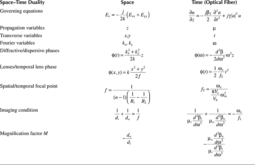
The space–time duality properties can be summarized as in Table 17.1.
Table 17.1 Space–Time Duality
The diffraction from an object by a lens produces an image which spatially dependent phase shift [18]. Figure 17.3 shows spatial imaging and temporal imaging systems [2,4]. The dispersion effects from an object pulse to lens and from lens to images are provided by two grating pairs that are installed before and after a quadratic phase modulator [10]. And this quadratic phase modulator acts as a time lens that provides a time-varying phase shift.
The equivalence between the diffraction–dispersion phase functions and space–time lens phase functions, between spatial domain and time domain, leads to the relationship between conventional spatial imaging and temporal imaging configurations, as summarized and described clearly in Figure 17.3a for spatial imaging and Figure 17.3b for temporal imaging. Let an unchirped pulse train enter into temporal and spatial imaging. First, these pulses would be distorted due to diffraction effect in space or dispersion effect in time. At this moment, the phase of each frequency component would be changed in the frequency domain, and therefore a time delay of these frequency components would occur in the time domain. Consequently, the pulse shape of these pulses is blurred or broadened. Next, these pulses are fed into a space lens or time lens. At this time, the carrier frequency is chirped up or down, depending on its applications. Last, this pulse train leaves a space or a time lens, and it is diffracted in the air or dispersed by a grating pair. This diffraction or dispersion is necessary and very important. The reason by all the frequency components of those pulses needed to be reorganized again in order to compress the input pulses due to their different time delays. Moreover, in order to expand or compress a pulse, the magnification parameter M should be modified. This magnification M could be changed by adjusting the object–lens distance, lens–image distance, or lens characteristics in space, or by changing the grating pair separation distance or quadratic phase modulator characteristic in time.

FIGURE 17.3 Configuration for (a) spatial imaging and (b) temporal imaging. (From B. H. Kolner, IEEE J. Quant. Electron., Vol. 30, No. 8, pp. 1951–1963, 1994; C. V. Bennett and B. H. Kolner, IEEE J. Quant. Electron., Vol. 36, No. 6, pp. 649–655, 2000.)
In particular, when these input pulses are compressed, the bit period is shortened. In order to avoid this problem, two thin lenses are used and separated by a mask, which plays the role of a Fourier transform plane. In a practical setup, a pulse train is transmitted to the fist lens, and these pulses are diffracted. A mask that includes an amplitude mask and a phase mask (called spatial light modulators), to control both the amplitude and phase of the pulse, could be used to yield any desired pulses. Finally, these pulses are refocused by a second lens. As a result, a received pulse train still keeps its original bit rate, while the pulse width of each individual pulse is reduced.
17.2.1.7 Electro-Optic Phase Modulator as a Time Lens
Electro-optic modulator is an optical device that is used to manipulating either the phase and/or amplitude of the light beam via the change of the refractive index of the medium by applying an electric field, the electro-optic effect. In this section, only phase modulation of the modulated beam is discussed. The electro-optic phase modulator lens has been used very popularly in pulse compression for ultra-short optical pulses, such as a few pico-seconds or a few hundred femto-seconds.
Khayim et al. [8] have introduced the relationship between the applied electric field corresponding to an electro-optic lens as well as the chirped optical carrier frequency, as shown in Figure 17.4 [8]. Furthermore, the focal length of the integrated guided wave electro-optic phase modulator can also be given as
where mask is the maximum width of the parabolic electrode; h is the spacing between the traveling wave electrodes; lo is the maximum length of the electrode; r33 is the electro-optic coefficient of the LiNbO3 Z-cut X-prop substrate; ne is the extraordinary index of refraction; and V(t) is the time-variable applied voltage.
Equation 17.18 and Figure 17.4 show that the convex or concave parabolic shape of an applied electric field corresponds to the diverging or converging lens and the down-chirping or up-chirping of the optical carrier frequency, respectively. Depending on specific applications, the carrier frequency would be chirped up or chirped down by adjusting the driving voltage applied to the electro-optic modulator in the time domain, which is equivalent to a converging or diverging lens in the spatial domain.

FIGURE 17.4 The relationship between phase modulator electric field, chirped carrier frequency, and corresponding lens. (From T. Khayim et al., IEEE J. Quant. Electron., Vol. 35, No. 10, pp. 1412–1418, 1999.)
17.2.2 Equalization in Transmission System
An ultra-high-speed optical transmission system is considered to be the essential backbone of the next generation of ultra-high-speed networks. When the pulse width reaches less than a few pico-seconds, not only second-order but even higher-order dispersion must be taken into account. On the contrary, third-order and higher-order dispersion effects are not fully compensated by using traditional dispersion-compensating devices such as DCF fibers. Moreover, ultra-fast transmission signals are very sensitive to environmental effects such as temperature, vibration, and so on. Thus, the received signals at receiver end would be distorted dramatically even if only a small outside factor affected the transmission link. Therefore, the tunable adaptive equalizer system is used at the receiver end to recover higher-order dispersion that could not be compensated by the DCF fiber, and to recover distorted signals to improve the BER or reduce the eye-opening penalty (EOP).
The structure of the equalizer system based on spatial and temporal imaging can offer useful and important applications of the time lens optical system, such as compensating GVD, third- and fourth-order dispersion, reducing the timing jitter for a pico-second pulse train, as well as time reversal with magnification [19,20]. Besides these, there are also a number of practical applications of time lens optical systems for temporal magnification and phase reversal optical data that are analogical to spatial diffraction and temporal dispersion [21]. It showed that space–time duality had valuable effects on ultra-fast photonic signal processing, and that its applications could be further explored in the mitigation of nonlinearity impairments. Adaptive dispersion equalization would become a key technique for ultra-high-speed transmission systems, and the temporal imaging theorem could be used to create this adaptive equalizer. Jannson [14] has realized that the spatial Fourier transformations of temporal signals are equivalent to the real-time Fourier transformations in dispersive optical fibers.
Initially, the temporal self-imaging effect in SMF and the time-domain Collett-Wolf equivalence theorem are studied and applied to the transference and propagation of the information contained in the periodic signals in fibers [22,23]. Consequently, this equalizer system model is built and developed based on the implementation of this well-known temporal imaging process. In this case, a single-mode optical fiber acted as free space in the spatial domain, and an adaptive equalizer acted as a time lens in the time domain. Following this quadratic phase modulator is a dispersive element that is used to change the phase of each frequency component in the frequency domain. Thus, different time delays appear between these frequency components, and the final pulse shape would be recovered. A standard SMF fiber link is used as a dispersive element (DCF or FBG could be used instead of using standard SMF fiber). This equalizer system, including quadratic phase modulator and SMF, is used to provide the required quadratic phase modulation [13]. Further investigations, theoretical calculations, and simulation results of transmission systems using adaptive equalizers are discussed in more detail in the later sections.
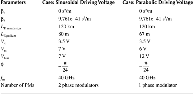
17.2.2.1 Equalization with Sinusoidal Driven Voltage Phase Modulator
For the optical fiber communication system, the GVD plays a significant role as it distorts signals dramatically, especially at ultra-high speeds. Also, the TOD effects or even the fourth-order dispersion effects also become more significant [24]. A combination of different fibers, such as SMF, reverse dispersion fiber, and DCF, would fully compensate for the second-order dispersion, but residual dispersion effects do exist. For ultra-fast transmitted signals, for example, at 160 Gbps, the system is very sensitive to the environmental effects such as the PMD and fluctuation of the dispersion factor. For example, if there is a small change in temperature, there would be a mismatch in compensation between SMF and DCF. This compensating mismatch would be accumulated over a long-haul transmission, and the received signals would be distorted randomly. Furthermore, for an installed transmission system, the TOD could not be eliminated by using DCF fiber for 160 Gbps transmitted signals. Therefore, an adaptive equalizer can equalize any distortion, adaptively with any variation of this impairment. It could compensate for second-, third-, and even fourth-order dispersion. Moreover, it also eliminated the timing jitter effect, and thus the BER at the receiver.
In order to investigate the effects of using an equalizer, some significant and necessary formulas are briefly given. In applying a sinusoidal driving voltage to phase modulator, a linear chirp would be generated, and hence amplitude distortion. The applied electric field would change the phase of each frequency component in the time domain, and thus the signal spectrum is broadened in the frequency domain. The transmitted signal at the output of the phase modulator is
The signal at the input of the receiver end would be the convolution between the signal at the output of the phase modulator and the dispersive device, the SSMF, and is given as
with D = β2LPM and . Assuming the chirping rate of the phase modulator , the received signal at the output of the equalizer can be obtained as
In order to recover the initial Gaussian pulse shape, condition should be applied to Equation 17.21 to obtain
If a sinusoidal driving voltage V(t) = Vbias + Vmcos(ωmt + ϕ) is applied to the phase modulator to chirp the carrier frequency of signals, then, by using the Taylor series expansion, and by the approximately quadratic driving voltage, the phase of the driving voltage would be
Comparing Equations 17.22 and 17.23, in order to recover the Gaussian pulse at the end of the system, a chirping rate should be . This depends on the amplitude of the driving voltage and modulation frequency . In a practical system, ωm could be tuned in order to achieve an almost reconstructed signal. Applying this sinusoidal time-dependent signal to a phase modulator in a 160 Gbps system with a full width at half maximum (FWHM) of an initial un-chirped pulse, TFWHM = 2 ps, and the corresponding input pulse half width at 1/e intensity point can be estimated as . Thus, the necessary chirping rate needed to recover the distorted signal is .
Assuming Vπ = 3.5V and Vbias = Vm = 7V so as to shift the sinusoidal wave up by Vm/2. Therefore, if a 40 GHz clock signal is used, the chirping rate becomes . Thus, two 40 GHz phase modulators must be employed to generate the required chirping rate. If the dispersion factor of standard SMF fiber is D = 17 ps/(nm.km), then the GVD coefficient would be β2 = −2.168e − 26 s2/m. Thus, the length of the SMF to be inserted in the equalizer would be calculated as .
17.2.2.2 Equalization with Parabolic Driven Voltage Phase Modulator
The transmission system including a phase equalization subsystem is shown in Figure 17.5.
Because a driving voltage has an ideal parabolic shape, it could create a parabolic phase. Because an SMF transfer function is H(f) = e−jαf2 [25], whose phase variation is parabolic. Therefore, an ideal parabolic driving voltage applied to a phase modulator, could fully equalize the distortion effects on the signals after the transmitting through the fiber link. If a parabolic driving voltage V(t) = Vbias − Vm(ωmt)2 is applied to the phase modulator instead of a purely sinusoidal driving voltage, then the phase variation at the output of this phase modulator becomes
A needed chirping rate for compensation at this time is , with a modulation frequency for the 160 Gbps bit rate system. The necessary parameters for compensation at this time are listed as: chirping rate K = 6.944 × 10²³ s−2, Vπ = 3.5V, Vm = 6V, Vbias = 2Vm = 12V, and SMF length in equalizer system is LPM ≈ 66.55m. The modulation frequency can be estimated as
In summary, if an ideal parabolic driving voltage is assumed, it is possible to achieve full compensation of all the distortions, and only one phase modulator can be used in this case. However, it is very difficult to generate an ideal parabolic driving voltage in practice. The received signals of sinusoidal variation can be acceptable, which could be generated easily. Thus, sinusoidal signal driving-signals applied to the phase modulator are presented in detail by simulation. The outcomes would be compared to the case when employing an ideal parabolic waveform.

FIGURE 17.5 The overview of the optical system communication by using an equalizer with ideal parabolic driving voltage.
17.3 Simulation of Transmission and Equalization
17.3.1 Single-Pulse Transmission
Simulation results are carried out for dispersion due to the mismatched lengths between SMF and DCM of the transmission links leading to distortion. Consequently, an adaptive equalizer should be installed at the end of the long-haul transmission link, especially at 160 Gbps, in order to fully compensate for all dispersion effects and timing jitter. Initially, a 2-ps-width single pulse is launched into the optical fiber. The distorted output pulse is monitored after propagating through a transmission link. Then this distorted pulse is led to the equalizer system for recovering its original pulse width and shape.
17.3.1.1 Equalization of Second-Order Dispersion
Figures 17.6 and 17.7 show the equalization of the second-order dispersion effect for a 2 ps Gaussian pulse transmission system.
Let us call To a pulse half width at e−1 intensity point. By calculating the second-order dispersion length , and TOD length km [26], with a group velocity coefficient β2 = −2.168e − 26 s2/m, and TOD coefficient β3 = 9.761e − 41 s3/m, the output pulse is obviously broadened dramatically if a length of transmission link is greater than LD3 in order to investigate a TOD effect. Table 17.2 tabulates the parameters of the equalizer required for the equalization of 160 Gbps transmission due to second- and TOD to demonstrate the effectiveness of the equalizer in the refocusing or reshaping of the transmitted signals.
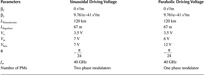
The simulated results tabulated in Table 17.2 show a strong consistency between estimation and simulation results. Figures 17.6a and 17.7a show the initial pulses before transmission through a 300 m optical fiber length under the two different waveforms of the applied voltage. These pulses would be spreading at the output of the receiver. The equalizer is inserted at the front end of the receiver in order to recover these distorted pulses to its original shape. On the contrary, the pulse shape observed after an equalizer with a sinusoidal driving voltage is not as closed to its original pulse shape with modulator driven by a parabolic driving voltage. The tails of recovered pulse is spreading over and can overlap with other tails from the adjacent pulses. This overlapping contributes to the penalty of the eye diagram. This effect can be observed due to the Taylor approximation, as assumed in Section 17.2. Due to the approximation of the parabolic shape in the region near t = 0, the Fourier transformed pulses have prolonged tails at the wings of pulse. This overlapping penalty is considered, discussed, and investigated further in Sections 17.4 and 17.5.
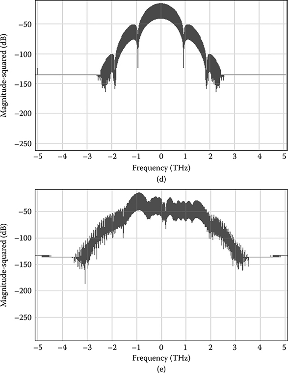
Figures 17.6d, e and 17.7d, e show the evolution of the spectrum of the pulses. The bandwidth of a spectrum before and after being transmitted through an optical fiber is the same, because the phase of each frequency component is changed in the frequency domain. These changes created a time delay of each carrier frequency component in the time domain, and thus the pulse is broadening. And carrier frequency is chirped down while transmitting through the SMF fiber. By using a phase modulator, the carrier frequency under pulse envelope is chirped up. The spectrum is also broadening at this step, because the phase of each frequency component is changed in the time domain, and it leads to a frequency delay in the frequency domain. Therefore, the envelope of these pulses is not changed, while the spectrum is expanded substantially.
Figures 17.6d through f and 17.7d through f plot the phase of the signal at the output of the SMF fiber, at the output of the phase modulator, and at the output of the equalizer. These phase plots indicate that the carrier frequency is chirped down or chirped up. Firstly, when a lightwave-modulated pulse propagating through SMF fiber, the carrier frequency is down chirped, thus carrier phase shape follows a convex parabolic function. However, the applied electric field is approximately concaved parabolic, and the carrier frequency would be chirped up. Only the phases of these frequency components are changed in the time domain, so the pulse shape remains the same. Then, carrier frequency is chirped down again when these pulses are transmitted through SMF in an equalizer.
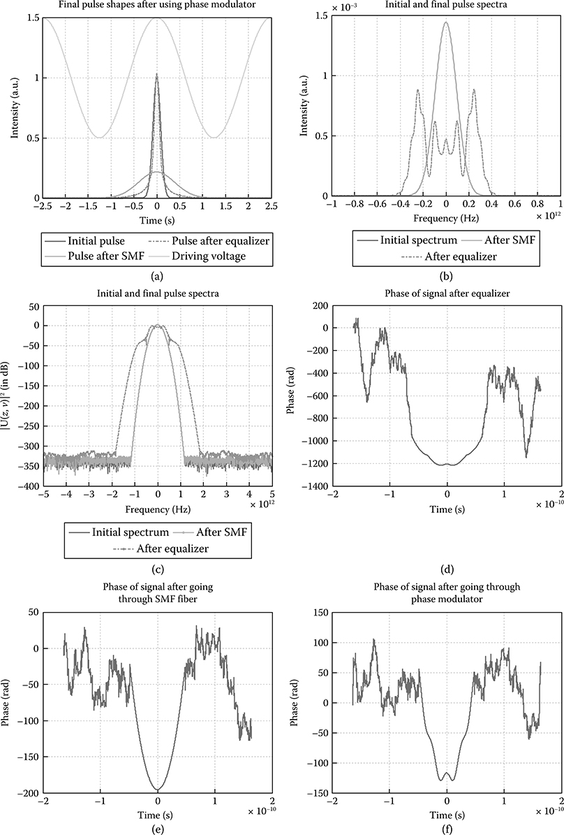
FIGURE 17.6 2 ps Gaussian pulse with a sinusoidal applied driving voltage.
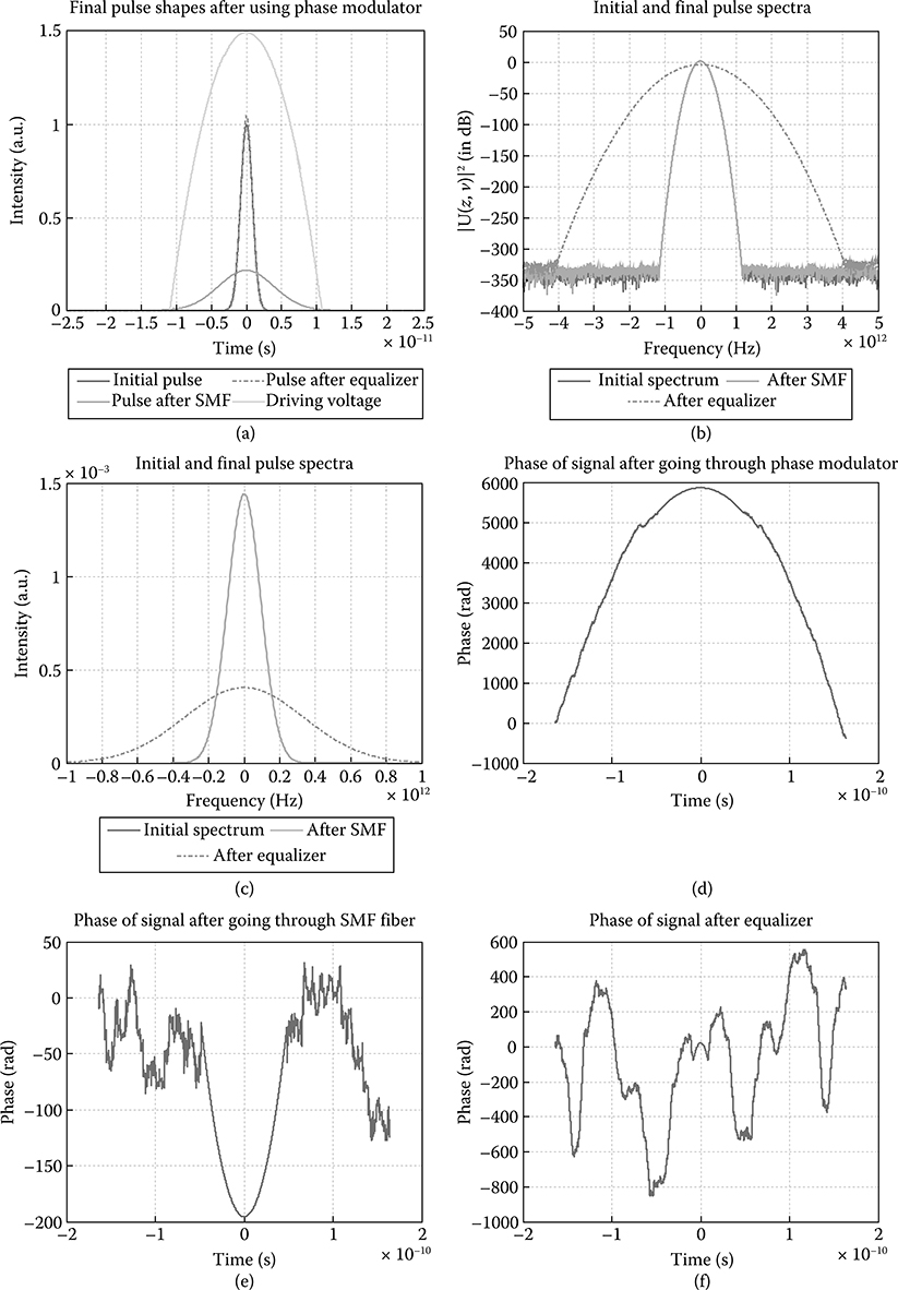
FIGURE 17.7 2 ps Gaussian pulse with parabolic applied driving voltage.
TABLE 17.2
Operation Parameters of the Equalization of the Second-Order Dispersion Effects on the Transmission of a Single Pulse

TABLE 17.3
Summary of Parameters for the Equalization of Third-Order Dispersion under Single-Pulse Transmission
During this process, there is a reorganization of each frequency component due to a different time delay of a different frequency component, and the output pulse shape would be recovered. Furthermore, attention should be paid when there is a little concave parabolic shape around the t = 0 area. It indicates that the carrier frequency under the pulse envelope is still chirped up. Thus, if the SMF length in the equalizer is increased, the output pulse from the equalizer would be even more compressed than the initial pulse.
In other words, the equalizer is a tunable system that could modify the output pulse width and its shape accordingly for changing some parameters in that equalizer such as voltage amplitude or SMF length.
17.3.1.2 Equalization of TOD
Table 17.3 shows all the necessary parameters for a TOD compensation in the cases where sinusoidal or parabolic driving voltages are used to drive the phase modulator. In this case, an electric field applied to a phase modulator is shifted right by an angle of π/24, due to the following reasons. First, the oscillated tail of this pulse should be covered by this driving voltage. Second, this distorted pulse is asymmetric, and TOD “pulls” a pulse to the right direction. If the driving voltage is still kept in the middle, as in the previous section, the phase of some frequency components might not be changed, or might be changed in the opposite way because the tail of the pulse spreads outside the concave parabolic curve of the driving voltage.

FIGURE 17.8 2 ps Gaussian pulse with sinusoidal applied driving voltage.
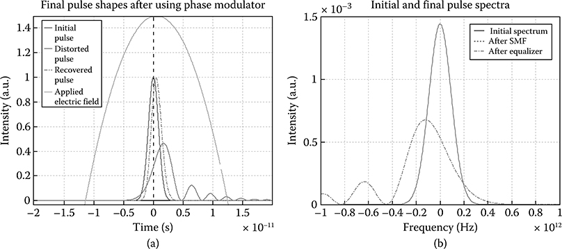
FIGURE 17.9 2 ps Gaussian pulse with parabolic applied driving voltage.
As shown in Figures 17.8a and 17.9a, the output pulse is almost fully recovered according to different voltage waveforms. However, for a transmitted pulse train, if the tail of the individual pulse can be broadened and spreading to neighboring pulses. This is the intersymbol interference and hence difficulty in the recovery of the original pulse states. Figures 17.8b and 17.9b are the spectral profiles corresponding to Figures 17.6a and 17.8a, respectively. It is seen clearly that the distortion in the time domain is converted to that in the frequency domain by Fourier transform, which has been discussed earlier.
17.3.2 Pulse Train Transmission
17.3.2.1 Second-Order Dispersion
Figures 17.10 and 17.11 show the propagating of a pulse train with a bit sequence [1 0 0 1 1 1 0 1], with 2 ps pulse width through 300 and 600 m optical fibers, respectively.

FIGURE 17.10 40 Gbps with 2 ps Gaussian pulse propagating through 300 m optical fiber with the sinusoidal driving voltage.
All other parameters remain the same for these two situations, and they are listed in Table 17.4.
Figures 17.10a and 17.11a show an initial and output pulse train after propagating through 300 and 600 m standard SMF fibers, respectively. The distorted pulse train is recovered and shown in Figures 17.10b and 17.11b. The corresponding spectrum to that pulse train is plotted in Figures 17.10c, d and 17.11c, d. Based on the transmission length of the SMF fiber, there is a huge difference between Figure 17.10 and Figure 17.11, which should be discussed thoroughly.
First of all, when this pulse train is transmitted through a 300 m fiber link, although each pulse in this pulse train is dispersed and broadened, their tails are still not overlapped with each other. Therefore, it is not a very big issue in compensating these dispersive pulses. The spectrum of this signal is also monitored, and it is obviously broadened to satisfy the expectation as explained before. Furthermore, there are several spikes, and the difference between each spike is about 40 GHz, which satisfies the theoretical calculation and expectation.
Since this pulse train is transmitted through 600 m optical fiber, the output pulse train is significantly distorted, and their tails overlap and pulses interfere one another. The overlapping between neighboring pulses would lead to constructive or destructive effects corresponding to the in-phase or out-of-phase status of those carrier frequencies, respectively. Therefore, there is an oscillation when the two tails of two neighboring pulses modulate to each other, as shown in Figure 17.11a. These oscillating tails would contribute to the noise and increase the noise levels of the optical system. Since the output after passing through the equalizer system is plotted in Figure 17.11b, the output pulse train had a significant improvement in dispersion compensation as well as noise reduction. Although total noise cancellation is not achieved since the driving voltage is just an approximated parabolic waveform, the existing noise level is also reduced significantly, and this noise level, after using an equalizer, is much less than before using it.

FIGURE 17.11 40 Gbps with 2 ps Gaussian pulse propagating through 600 m optical fiber with the sinusoidal driving voltage.
TABLE 17.4
Parameters for Equalization of Second-Order Elimination under Pulse Train Transmission

17.3.2.2 Equalization of TOD
Figure 17.12a and b shows the initial, distorted, and recovered pulse train after transmitting through a 120 km transmission link, while Figure 17.12c and d shows the spectrum corresponding to that pulse train, respectively. This distorted pulse train, recovered by using an equalizer system and this recovering phenomenon, is discussed clearly in Section 17.3.1.2.
On the contrary, a pulse train is investigated because there are some effects that cannot be obtained or monitored by using a single pulse such as a timing jitter effect. When there are neighboring pulses, two closed pulses will be pulled or pushed from their original position due to reasons such as TOD, nonlinearity effects, and so on. Thus, this effect contributes to the worsening of the BER of transmission systems. One of the most severe influence of this nonlinear effect is the jitter of the pulse sequence by its low frequency modulation, this leads to errors in the clock sampling at the receiver and thus the error rate. Therefore, the received signals would not be correct and reliable anymore.
FIGURE 17.12 40 Gbps with 2 ps Gaussian pulse propagating through 120 km optical fiber with the sinusoidal driving voltage.
In order to eliminate this problem, an equalizer would be used to push or pull these pulses back to their initial positions as well as remove their distortion. Section 17.3.3 presents further discussions with some simulation results about timing jitter elimination.
17.3.3 Equalization of Timing Jitter and PMD
PMD is a form of modal dispersion where two different polarizations of light in a waveguide, which normally travel at the same speed, travel at different speeds. Thus, it would become broader as the two components disperse along the fiber due to their different group velocities, random imperfections, and asymmetries. In a fiber with constant birefringence, pulse broadening could be estimated from the time delay between two polarization components during propagation of the pulse, where x and y are the two orthogonally polarized modes, Vg is group velocity, and L is a transmission length [27]. There are several PMD compensation schemes using a polarization controller and a phase modulator in the transmitter [9], or using “time lens” [28]. These PMD compensation schemes show that pulses that are placed at different times due to PMD could be shifted into their right positions. Consequently, timing jitter owing to PMD dispersion or other reasons such as nonlinearity effect could also be eliminated. It is pointed out that timing jitter suppression could be applied by using the preceding PMD compensation schemes, as has been proven by Howe and Xu [29] and Jiang [30].
Temporal imaging theorem could be applied in this situation to eliminate timing jitter and PMD. In particular, the phase modulator would apply a very high chirping rate, which could dominate all existing chirping rates owing to PMD, nonlinear effect, and second- and third-order dispersion. Then these pulses with high chirping carrier frequencies are transmitted through the optical fiber link to compress their pulse, recover their original pulse shape, and pull those pulses distorted by timing jitter or PMD back to their original positions.
Figure 17.13 shows timing jitter elimination by using phase modulation with sinusoidal applied voltage, ideal parabolic voltage, and spectral profile corresponding to those recovered pulses. Table 17.5 outlines all parameters of the third order nonlinear coefficients. Table 17.6 indicates all setting necessary parameters in the equalizer system for timing jitter and PMD elimination.
Figure 17.13a shows the timing shift in a range of about ±4 ps added to the input signals with PMD and TOD distortion. The recovered pulse is plotted in Figure 17.13b and c, with sinusoidal applied voltage and ideal parabolic voltage, respectively. The spectral profiles are also plotted in Figure 17.13d and e, corresponding to Figure 17.13b and c, respectively.
When a driving voltage had a sinusoidal waveform, the jittered pulse could not be fully recovered to its original pulse shape. With respect to parabolic modulation, a jittered pulse is fully recovered from TOD and pulled back to its original position. Therefore, it is difficult to fully reduce timing jitter and PMD under sinusoidal modulation, especially when the jittered pulse is broadened within the whole curvature of the modulation. However, under a reasonable jitter or PMD, it is very possible to compensate and pull it back to its original form.
The ideal situation is to use ideal parabolic modulation to fully recover pulse. However, there is a tradeoff between using parabolic and sinusoidal applied voltages. First, it is very hard to generate an ideal parabolic waveform in practice. Second, if it were possible to build a parabolic driving voltage, it would be expensive compared to the very popular sinusoidal waveform. Third, if jittered or PMD pulses are still in a reasonable range, they could still be recovered and pulled back to their initial position with reasonable achieved results. In conclusion, depending on to use either a sinusoidal driving voltage or extensive efforts to generate an ideal or closed to ideal parabolic modulation, the equalization can be approximately implemented. The remaining dispersion or distortion can be subsequently compensated in either the optical or digital electronic domain.
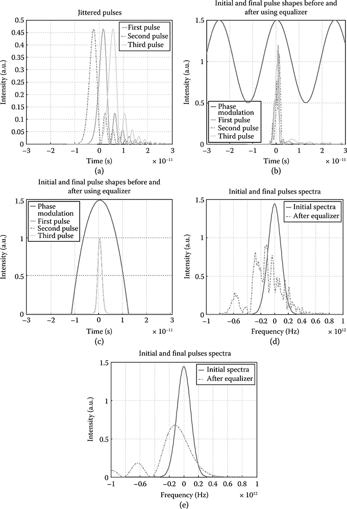
FIGURE 17.13 Investigation of three jittered 2 ps Gaussian pulses.
TABLE 17.5
Parameters for Equalization of Third-Order Elimination under Pulse Train Transmission

TABLE 17.6
Summary of Timing Jitter Elimination Parameters
17.4 Equalization in 160 Gbps Transmission System
17.4.1 System Overview
17.4.1.1 System Configurations
Recently, an SSMF with a GVD value of about 17 ps/(nm · km) has been used widely in long-haul transmission. As discussed earlier, DCF is one of the dispersion management methods to recover signals after a multispan transmission link. However, dispersion slope compensation and wavelength division multiplexed transmission is very hard to be fully compensated, especially for ultra-fast transmitted signals. For example, it would return a significant variation in transmission performance for 160 Gbps, even though there is only a small change in dispersion due to environmental or setting up effects. Therefore, the equalizer system, which includes two main devices—the phase modulator followed by a dispersive element—is used before the receiver. This equalizer is used to compensate not only for GVD but also for third- or fourth-order dispersion [24,31], and also timing jitter [30].
In this study, the equalizer system is used for one span of 120 km transmission fiber (including standard SMF and DCF) to compensate for a GVD of 1.28 ps/nm and a TOD of 1.692 ps/nm2. Furthermore, the BER is also calculated when the equalizer is and is not installed, in order to prove the critical improvement when an equalizer is used in the system. In order to investigate the limitation of a 160 Gbps system with and without an equalizer by increasing the number of spans, the transmission length would be increased for each situation. Eye diagrams are also plotted for each situation at a value of receiver power of approximately −32 dBm. From those eye diagrams, significant improvement will be seen for the transmitted system with an equalizer, especially when the number of spans is increased more and more.
17.4.1.2 Experimental Setup
First of all, in order to generate a 160 Gbps optical time division multiplexing (OTDM) signal, a 10 GHz pulse train is created from a mode-locked fiber laser [32], which is modulated at 10 Gbps and then multiplexed optically to 160 Gbps [12,33]. This 160 Gpbs OTDM signal would be transmitted through one span that is a 120 km transmission link, which includes standard SMF and DCF fibers. Afterward, this transmitted signal is demultiplexed to a 10 Gbps signal. Figures 17.14 and 17.15 show the experimental setup with and without an equalizer [12,33].
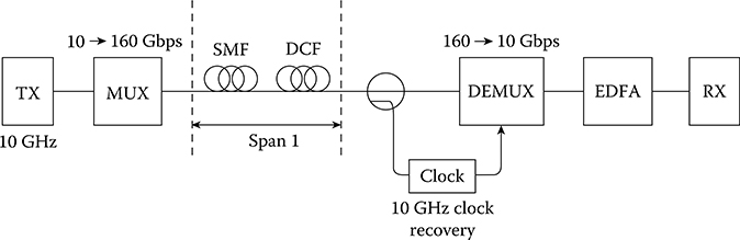
FIGURE 17.14 160 Gbps transmission setup without equalizer.
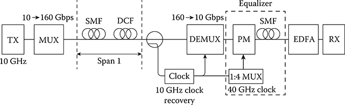
FIGURE 17.15 160 Gbps transmission setup with equalizer. (From T. Hirooka et al., IEEE Photon. Technol. Lett., Vol. 16, No. 10, pp. 2371–2373, 2004; T. Hirooka and M. Nakazawa, J. Lightwave Technol., Vol. 24, No. 7, pp. 2530–2540, 2006.)
The equalizer system includes a phase modulator that is used to modify the chirping factor of carrier frequency, followed by a standard SMF to reshape a received signal, as discussed in the previous section. In addition, a 40 GHz recovery clock is chosen to drive the phase modulator, and this choice is calculated in Section 17.2. Owing to limitation of time, equipment, and experimental knowledge, this experimental setup is applied in a simulation model for further investigation. The Simulink platform is chosen because of its so many advantages. First of all, MATLAB is the standard mathematical tool in academic and R&D laboratories. It is also a very useful and powerful tool for simulation. Furthermore, several existing packages have already been developed for teaching and research purposes, and they are adapted and modified for this simulation purpose. Finally, individual Simulink blocks could be reused and applied for other Simulink models without any conflicts between these models.
Because of the huge advantages of using the Simulink model in MATLAB for running simulations, this platform has been chosen to build a 160 Gbps transmitted signal system with and without an equalizer, based on a real experimental setup. Section 17.4.2 is devoted to introducing and building Simulink models and parameter setting for this study.
17.4.2 Simulation Model Overview
17.4.2.1 System Overview
Modeling of an optical communication system that satisfies some requirements such as simplicity, accuracy in terms of phenomena, and corroborating with experimental systems is very important. Thus, this Simulink model is adapted and modified from some existing Simulink blocks, and they are used, and modified, and thus some new Simulink blocks can be developed. Together, they would create a necessary 160 Gbps system that is built up based on a real experimental setup, which has been introduced briefly in the preceding text (Figure 17.16).
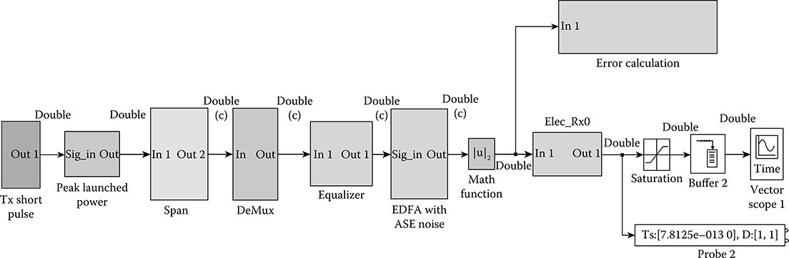
FIGURE 17.16 Overview of Simulink® model for an optical communication system.
The purpose of this Simulink model is to investigate GVD and TOD effects in ultra-fast signal processing. Only an equalization process in linear regime is considered at this stage, and any nonlinearity effects are negligible. Actually, nonlinear effects might change the phase of each frequency component, and it would create a chirp rate on optical carrier frequency. However, the chirp rate that is created from a nonlinear effect is sufficiently small compared to the chirp rate generated from a phase modulator. Thus, it is reasonable to eliminate nonlinearity effect at this stage. This section concentrates on explaining and developing a Simulink model that could be capable of simulating a dispersive compensation before and after using an adaptive equalizer. Some achieved results are also demonstrated in this section.
First of all, a transmitter that could generate 160 Gbps signals transmitted data through fibers at 10 dBm peak power. Although this launching power is high enough to have nonlinearity effects during transmitting signals, it is still ignored, owing to the preceding explanations. Assuming that only one span of transmission fibers of SSMF plus DCF, is employed in the transmission links, is used in these transmission links. When the signal is launched through an SMF fiber, GVD and TOD would affect the propagation signal, and the output signal would be distorted dramatically. Although DCF is used for compensation, the final output signal would not be fully recovered due to other factors such as TOD, PMD, timing jitter, and so on. These problems are also analyzed and discussed in more detail in Sections 17.2 and 17.5, which are devoted to presenting some simulation results about those dispersive effects and their eliminations.
Because the speed of 160 Gbps source is so high that it is currently not yet available, the high-speed OTDM technique would be used to generate this high transmission rate. 160 Gbps or even higher bit rates have already been introduced and generated by using a 10 GHz regenerative mode-locked fiber laser [34,35 and 36]. Consequently, this Simulink 160 Gbps laser source is built based on this OTDM technique.
Initially, 16 transmitters of 10 Gbps are used, and these 16 10 Gbps signals are multiplexed by using the OTDM technique. This high-speed signal is transmitted to 120 km (one span), and to several spans of transmission links at later stages. Because the transmitted signals are multiplexed before launching through the optical fiber, they should be demultiplexed back into a 10 Gbps signal. This demultiplexed signal is fed into an equalizer system to recover distorted signals. Erbium-doped fiber is also used to amplify the output signal from the equalizer before receiving this signal at the receiver end. Moreover, an error calculation block is also inserted right before the receiver block in order to count the errors that would be used for calculating BER by the Monte Carlo method. An eye diagram is also plotted as inserted in a pop-up window when the simulation starts running.
17.4.2.2 Transmitter Block
The transmitter is always a necessary device in any communication system. An optical transmitter source is used to launch a laser beam into an optical fiber in a transmission system. This laser beam carries transmitted data that is modulated under different modulation formats such as non-return-to-zero (NRZ), minimum shift keying (MSK), phase shift keying (PSK), and so on, and the return-to-zero (RZ) format is chosen to use in this investigation. The optical transmitter block is shown in Figure 17.1.
A pulse generator block is used to generate a 10 GHz square wave with a 2 ps pulse width. The parameters of the pulse generator are set with (1) pulse amplitude = 1; (2) pulse period = 100 ps; and (3) pulse width = 2 ps, that is, about 2% of the pulse period.
Then, this square wave is fed into the MUX block in order to generate 160 GHz square wave transmitted signals. Figure 17.17 shows that a 10 GHz square wave from the pulse generator block is split into 16 input square waves with different time delays by using the transport delay block. This time delay could be created by using a microring with different lengths in an experimental setup. Furthermore, this MUX block also included 16 Bernoulli random sources that are considered as 16 different transmitting data signals. These 16 different data signals are multiplied with the square waves mentioned earlier, and these multiplication results are added up to generate 160 Gbps square wave signals afterward. This output square wave signal has been filtered by using a Gaussian filter to generate a 160 Gbps Gaussian-pulse-shaped signal that is launched into a transmission link under the RZ format at 10 dBm peak launched power. The 160 Gbps Gaussian output multiplexed signal is shown in Figure 17.18.
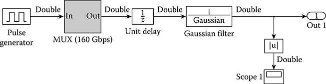
FIGURE 17.17 Transmitter Simulink® model.
In order to compare between transmitted and received signals for BER calculation, a “Goto” tag is added to the scope block. In the experimental setup, this multiplexed signal would be demultiplexed into 16 different data packets at the receiver end, and these data packets have been detected at the receiver. When a data packet is extracted and processed in this Simulink model, it is saved via the Goto tag and sent to the error calculation block for comparison at the receiver end.
17.4.2.3 Transmission Link
The schematic representations, both in subsystem blocks and in the Simulink of a 120 km transmission link, including SMF-DCF fibers, is described in Figures 17.15 and 17.16, respectively. The 160 Gbps RZ transmitted signals of Gaussian shape are launched into a 98 km SSMF at a 10 dBm peak power (Figure 17.19). DCF is used for GVD compensation. Oscilloscopes and spectrum scopes are inserted in front of the SMF, between the SMF and the DCF fiber, and after the DCF fiber in order to observe and measure the pulse broadening as well as compensating factors during a transmission (Figure 17.20). Pulses and spectral profiles are analyzed and discussed in detail in the following section.
17.4.2.4 Demultiplexer
At the receiver end, the 160 Gbps transmitted signals are demultiplexed to a 10 Gbps signal after passing through a demultiplexer block. A 10 GHz clock recovery has been applied to the demultiplexer block. This clock generated a 10 GHz square wave with a 6.25 ps pulse width. The purpose of this clock recovery is illustrated in a simple demultiplexed example in Figure 17.21.
Assuming that 30 Gbps OTDM multiplexed signal to be demultiplexed to 10 Gbps sequence at the receiver end of a transmission system, then the blocks of demultiplexer, clock one and two are used to recover the first, second, and third demultiplexed sequences, respectively, by multiplying this multiplexed signal with each clock recovery. Likewise, synchronization is also an important factor that must be taken into account. Therefore, a unit delay is added in this DeMux block for synchronization purposes, as shown in Figure 17.22. The pulse generator, which acts as a clock recovery, is used to generate a 10 GHz square wave with 6.25 ps pulse width. This square wave is delayed by feeding into the unit delay block, and then multiplied with the input signal for the demultiplexing process.
Figure 17.23 demonstrates an example of a successful demultiplexed signal after passing through the DeMux block. The higher-position scope (Scope 1) shows the original multiplexed signal, and the demultiplexed output signal is plotted on the lower scope (Scope 3). According to the input signal, the output signal is successfully demultiplexed. In addition, the synchronization issue is even more harder and more significant when TOD and time jittering effects play a critical role during propagation through the transmission link. Thus, a clock should be synchronized with suitable pulses accurately in order to sample the correct bits.
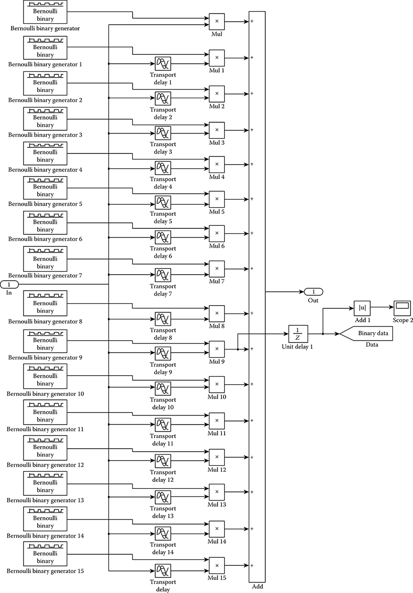
FIGURE 17.18 Multiplexer model with 16 different wavelength sources.
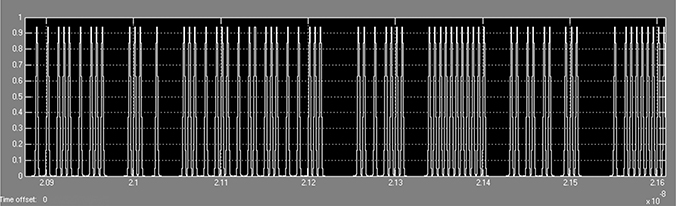
FIGURE 17.19 160 Gbps OTDM output signal.
17.4.2.5 Equalizer System
The equalizer system that has been invented according to the temporal imaging theorem has been introduced and discussed clearly on working algorithms as well as some demonstrated simulation results in the previous sections. This equalizer included a phase modulator, followed by a dispersive element, which is a standard SMF fiber in this Simulink model. Figure 17.24 shows the structure of the subsystem model. The working algorithm of the equalizer system has already been discussed in detail in the previous section. Thus, this section concentrates more on how to build this Simulink model, setting up parameters and some significant results in the sections that follow. The main function of the phase modulator in this model is to create a required chirping-rate-to-carrier frequency of the optical signal. By applying a driving voltage to a phase modulator, the optical signal would be phase modulated because the optical path length is altered by the electric field. Figure 17.24 shows a phase modulator block in more detail, and it reveals the previously explained phase modulation concept.
This phase modulator block includes a sinusoidal source to generate a 40 GHz sinusoidal wave to drive a phase modulator. Let Vπ be the voltage applied to generate a π phase shift on the optical carrier frequency. Basing on some formulas derived in Section 17.3, a term is multiplied into that sinusoidal waveform. As with all calculations in Section 17.3, the amplitude of the driving voltage Vm is set to 7 V, which is double the value 3.5 V of Vπ, in order to achieve a 2π phase shift on carrier frequency to guarantee the necessary chirp rate. Furthermore, two 40 GHz phase modulators are used in this situation to recover the output signal as a theoretical calculation in Section 17.3 and simulation results in Section 17.4. Thus, the multiplication product is a result of three multiplications between two 40 GHz phase modulators and input signals.
In addition, the synchronization issue is very important, because each output Gaussian pulse of the transmitted data must be fully covered by this 40 GHz sinusoidal driving voltage. It is a necessary process because all optical carrier frequencies need to be chirped correctly by this applied electric field. At this stage, Scope 1 and Scope 2 in Figure 17.25 are used to monitor the applied electric field and input signal, to confirm that the phases of each pulse of signal and sinusoidal waveform is in-phase. Otherwise, the driving voltage should be tuned until an expected position is achieved. This Simulink setup model is also based on the experimental setup described in Section 17.4.1.2. If all the parameters are set correctly, this driving voltage would directly change the phase of each frequency component of the input signal. As a result, the chirping rate of the carrier frequency of this signal had to be changed, and this carrier frequency has been set to be chirped up as the theoretical calculation. These pulses would be compressed and recovered after propagating through an SMF fiber in this model due to reorganization frequency components during the propagation process.
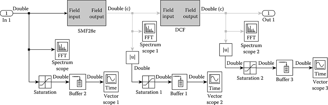
FIGURE 17.20 SMF–DCF fiber in one transmission span.
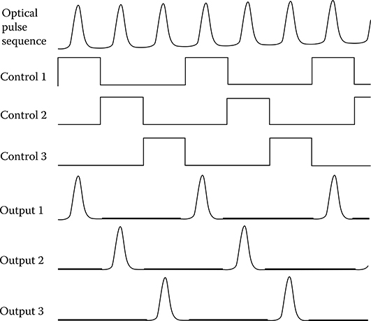
FIGURE 17.21 Optical pulse sequence and control applied signals to demultiplexers and the corresponding outputs.

FIGURE 17.22 Demultiplexer block in detail.
17.4.2.6 Errors Calculation
First, this errors calculation block is built to calculate the BER based on the Monte Carlo method, which is a widely used class of computational algorithms for simulating the behavior of systems. Furthermore, the Monte Carlo method is employed since it is useful for modeling phenomena with significant uncertainty in inputs. Figure 17.26 shows a BER calculation block using the Monte Carlo method.
The threshold time decision binary detection (TTDBD) block is adapted and modified to detect between bit 1 and bit 0 of the received signal. The output from TTDBD is connected to the error rate calculation (ERC) block to calculate the BER and the find delay block to set the time delay between signals from the transmitter end (from the “Binarydata” tag, which is collected from the transmitter block) and the receiver end to the integer delay block. The purpose of the find delay block is to synchronize between transmitted and received signals.
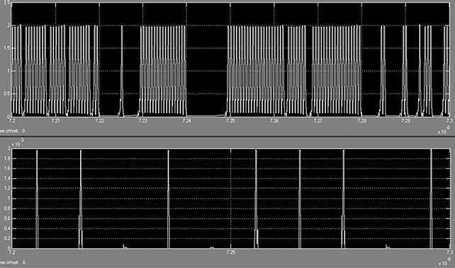
FIGURE 17.23 Demultiplexed signal.
Finally, the computational delay in the ERC block should be set with the same value as the value from find delay block. For example, a number “1794,” which is returned from find delay block, should be set for the integer delay block. As a result, the ERC block should also ignore the first 1794 samples at the beginning of the comparison in this block. It follows that this number should obviously be set for a computation delay parameter. In addition, the correlation window length (samples) parameter of the find delay block should be set sufficiently large so that the computed delay eventually stabilizes at a constant value. However, there is a tradeoff between the reliability of the computed delay and the processing time to compute the delay. Thus, a reasonable value for the correlation window length should also be taken into account.
17.4.3 Simulation Results
17.4.3.1 Single-Pulse Transmission
17.4.3.1.1 Equalization of Distortion Due to GVD
The Simulink model for this GVD elimination is modified a bit to cope with the purpose of this section. The transmitter is used temporarily to transmit a single pulse, and thus the multiplexer and demultiplexer blocks are taken out. Furthermore, only 300 m of SMF fiber is used in this transmission link, and DCF is not necessarily used in this section.
With respect to the pulse shape of a single pulse of the transmitter output from the oscilloscope, the full width at the half maximum of this single pulse is measured to be approximately 2 ps (Figure 17.27a). After propagating through 300 m of standard SMF fiber, this pulse is broadened to about 9 ps (Figure 17.27b). This achieved result is consistent with the simulation result in Section 17.3 and the theoretical calculation. The final recovered pulse shape is plotted in Figure 17.27c with a pulse width value of 2 ps, but it had a longer tail as compared to the original pulse shape.
In addition, the spectral profiles of a single pulse before and after using the equalizer are shown in Figure 17.27d and e. The spectrum of a lightwave-modulated single pulse before and after propagating through a SMF fiber remain the same, because only the phases of the spectral components are changed. Thus these phase changes superimpose different time delays on each individual spectral component due to the wavelength dependent of the effective indexes of the guided lightwaves. Moreover, these delays are a reason for pulse broadening. Compared to the spectra after the equalizer that is broadened dramatically, it indicates that the optical carrier frequency is chirped, and it is actually up-chirped, which is consistent with theoretical calculations and expectations.

FIGURE 17.24 Equalizer system including phase modulator followed by an SMF.
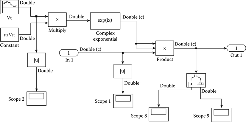
FIGURE 17.25 Phase modulator block in detail.

FIGURE 17.26 The BER calculation block.
Finally, all simulation results for a transmitted single pulse have matched with the obtained results from Section 17.4 and the expectations. Therefore, an equalizer could eliminate the GVD effect during transmission.
17.4.3.1.2 TOD Elimination
TOD plays a significant role in ultra-high-speed signals in the transmission system. From theoretical calculation and simulation results from Sections 17.2 and 17.3, respectively, sinusoidal modulation would not have fully recovered the distorted signals due to their asymmetric TOD. On the contrary, the oscillated tail of the recovered signal is a reasonable reduction, and thus the noise level created from this tail does not have a big effect on the transmission system, and its contribution to BER is acceptable. Figure 17.28a through c shows an initial single pulse before being transmitted through the optical fiber, a distorted pulse that is affected critically by TOD after propagating through a 120 km transmission link, and recovered pulse after the equalizer, respectively. Figure 17.28d and e plots the spectra of this single pulse before and after the equalizer. It shows that the carrier frequency is chirped at a very high chirping rate, which dominates all other effects such as nonlinearity of the second-order, third-order, jitter, or PMD effects.

FIGURE 17.27 GVD effects under single-pulse transmission: (a) at a transmitter; (b) after 300 m SMF; (c) after equalizer; (d) and (e) spectral profile of a single pulse before and after the equalizer, respectively.
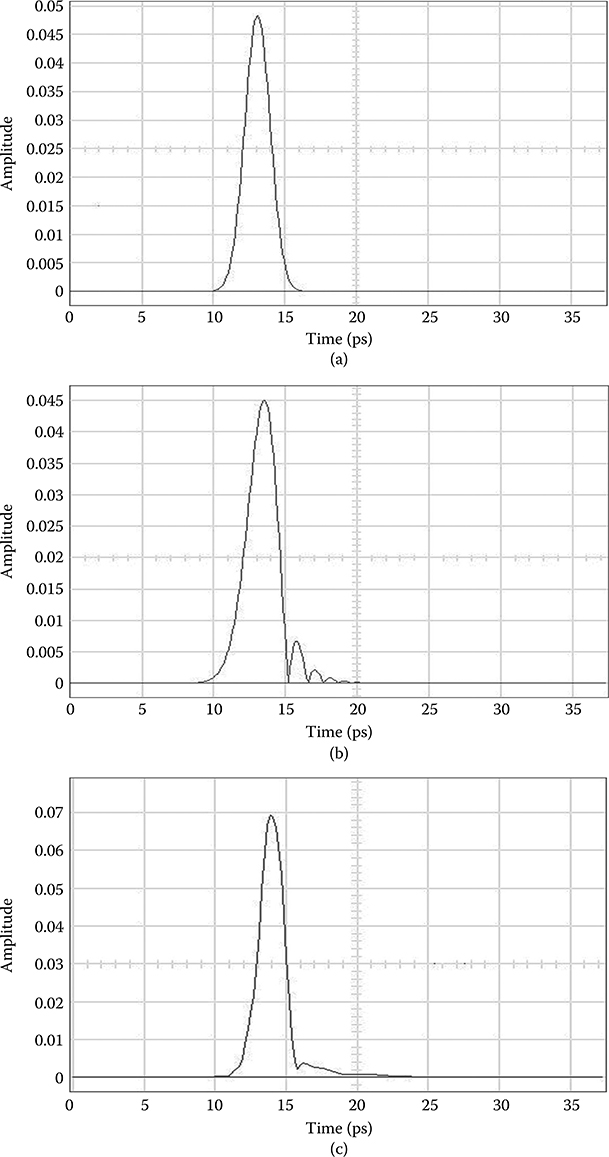
FIGURE 17.28 TOD elimination for a single-pulse transmission (a) at a transmitter; (b) after 120 km SMF; (c) after the equalizer. (d) and (e) spectral profiles before and after the equalizer, respectively.
17.4.3.2 160 Gbps Transmission and Equalization
Ultra-high-speed communication systems have been becoming more and more popular because of the increase in demand for high-capacity optical networks. Furthermore, transmission distance for this ultra-fast transmitted signal is improving and developing. In order to achieve longer transmission links with high-speed transmission, different modulation formats such as differential PSK is applied [37]. For the OTDM system, use of the on–off keying format has been extended up to approximately 600 km transmission distance. The limit of the OTDM technique is that, due to its sensitivity properties, even small perturbations in the optical fibers such as GVD, TOD, PMD, and timing jitter could distort signals dramatically [38,39]. In this section, some significant results are given for a 120 km transmission link with BER characteristics. The transmission length is a parameter for the evaluation of the equalized system, and the eye diagram is illustrated for the received power of about −32 dBm.
17.4.3.2.1 GVD Equalization of 120 km SSMF Transmission
Simulation results for GVD equalization are shown in Table 17.7 for three situations: back-to-back (transmitter and receiver are connected directly together without a transmission link), without equalizer, and with equalizer. These data are then plotted in Figure 17.29 with a GVD value of 1.28 ps/nm. The TOD, nonlinear effect, and timing jitter are set to zero in order to investigate only the GVD effect.
In this simulation setup, a 97.84 km standard SMF fiber with dispersion parameter D = 17 ps/(nm · km) is used as the transmission link. In order to have a second-order dispersion compensation, a 22.16 km DCF fiber length is used, with dispersion parameter D = −75 ps/(nm · km). Therefore, a GVD value of 1.28 ps/nm is the mismatched dispersion.
TABLE 17.7
BER Characteristic for GVD Equalization of 160 Gbps System for Back-to-Back, with and without Equalizer


FIGURE 17.29 BER versus receiver sensitivity of 10 Gbps demultiplexing signal under GVD linear impairment under the case of back-to-back “triangle.”; transmission with “square”; and without equalizer “diamond.”
With a low value of received power, there is an improvement of about 1/2 dBm between with and without an equalizer at a log(BER) value of −5. However, this difference is increased when the received power is increased. For example, at a log(BER) value of −8, this improvement is greater than 1 dBm. This is further improved as a function of the receiver sensitivity. Thus, using an equalizer could improve long-haul transmission performance, especially at a higher received power (or at a higher signal-to-noise ratio).
The back-to-back BER characteristic is also plotted in Figure 17.29. Although the improvement of the EOP for using the equalizer is still approximately half a dBm worse than the back-to-back system, it still shows a better improvement when the equalizer is used. This small residual penalty is due to the approximation of using a sinusoidal waveform instead of an ideal parabolic waveform. If the received power is increased further, there would be a significant BER improvement, with saturation at around −32. Thus, the error floor would appear following a diamond-trend at the higher received power value.
Figure 17.30 shows eye diagrams corresponding to the individual curve of the BER transmission performance. For example, Figure 17.30a1 shows an eye diagram in the case before demultiplexing, and Figure 17.30a2 and a3 shows eye diagrams after demultiplexing at the received power values of −36.375 and −36.745 dBm under without and with equalizer, respectively. Before demultiplexing, the input signals of 160 Gbps are observed as depicted in Figure 17.30(a1). The middle and right-hand-side eye diagrams (a2) and (a3) are the demultiplexed 10 Gbps signals at the receiver end under without and with equalizer, respectively.
Through the eye diagrams obtained for different received power levels, it is observed that higher the received power, the more the opening of the eye. The FWHM of the distorted eye is about 3 ps, while the FWHM of the recovered eye is only approximately 2 ps at about −32 dBm received power. Thus, there is a significant improvement when the equalizer is inserted, especially in long-haul transmission under accumulation of mismatched dispersion.
17.4.3.2.2 TOD Equalization of 120 km SSMF Transmission
For TOD elimination case, a second-order dispersion is assumed to be fully compensated by the DCF fiber. A 104.7 km standard SMF and a 15.3 km DCF with dispersion slope values of S = 0.06 ps/ (nm2 . km) and 15.3 ps/(nm2 . km), respectively, are used in each span of the transmission system. Thus, the dispersion slope TOD is calculated with a value of about 1.692 ps/nm2.
Table 17.8 and Figure 17.31 show the simulation results, the BER characteristics of the TOD equalization scheme. Although the TOD effect for 120 km is not very significant when compared to the GVD effect, as discussed in the previous section, the equalizer still shows its usefulness in improving transmission performance. However, this BER characteristic when using the equalizer could still not get closer to the back-to-back line (triangle line). The error floor is possible due to the diamond line for nonequalization at a higher received power, while a square-line for using the equalizer system still drops steeply. Consequently, the improvement between using and not using an equalizer would be much greater than 1 dBm (as at about log(BER) = −8 in Figure 17.31).
In conclusion, an equalizer offers significant improvement of the transmission performance in long-haul optical transmissions. Furthermore, when the signal-to-noise ratio is improved, there is a significant improvement between using and not using an equalizer system. Some eye diagrams are also plotted in Figure 17.32.
Figure 17.32a1, a2, and a3 shows eye diagrams for 160 Gbps signals before being demultiplexed, 10 Gbps signals after being demultiplexed not using equalizer, and 10 Gbps signals after being demultiplexed using equalizer, respectively, and, from (a) to (e), showed eye diagrams for each received power values from simulation. There is an improvement when a higher power is received at the receiver end. Furthermore, with the same received power value, eye diagrams in the TOD case are a bit bigger than the eye diagrams in the GVD case. Therefore, a received BER from simulation also showed lower BER values in the TOD case for a case using an equalizer. Although the BER of the system remained pretty much the same as the GVD elimination due to the approximation of sinusoidal applied voltage, it still confirmed its usefulness in compensating for second-order and third-order effects (might also be timing jitter and PMD during transmission) through Figures 17.30 and 17.32. Furthermore, the FWHM of the distorted eye is about 2.8 ps, while the FWHM of the recovered eye is approximately 2.2 ps at the received power value of about −32 dBm.
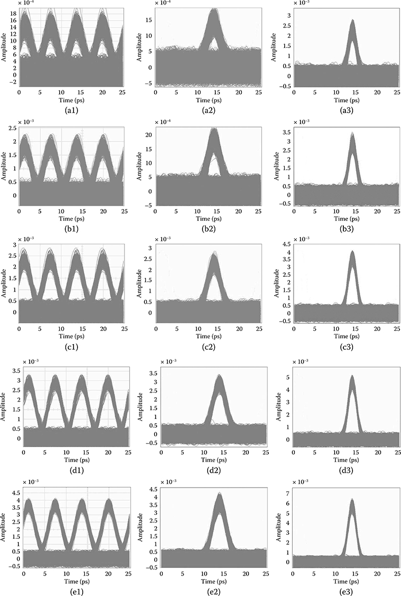
FIGURE 17.30 Eye diagrams monitored at different locations along the optical transmission lines under without and with GVD effects and with different received power for three cases (from left to right): before demultiplexing, after demultiplexing without and with equalizer.
TABLE 17.8
BER Characteristic Summary of TOD Elimination for 160 Gbps System for Back-to-Back, with and without Equalizer

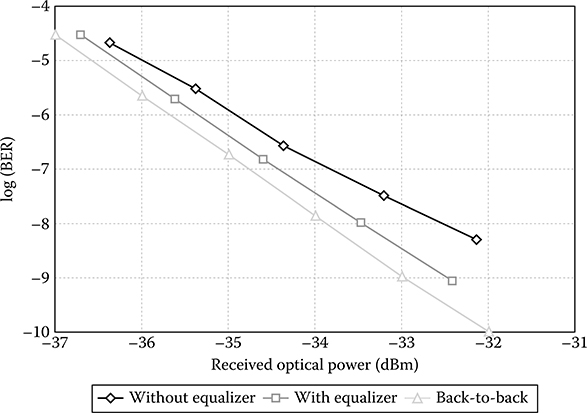
FIGURE 17.31 BER versus receiver sensitivity of 10 Gbps demultiplexing signal in TOD elimination under the case of back-to-back “triangle.” and transmission with “square” and without equalizer “diamond.”
17.4.3.2.3 Equalization of TOD with Variable Fiber Lengths
The TOD effects critically impose the distortion of the pulse transmission over the long-haul transmission link. Unlike the effect of the GVD that could be fully compensated for by using the DCF fiber, it is very difficult to compensate for TOD fully by using existing DCFs. Therefore, there is always distortion due to the mismatch between SMFs and DCFs. To compensate for the TOD, the equalizer offers some additional equalization potential that may be necessary at the end of the transmission system.
The five pairs of eye diagrams in Figure 17.33 show the recovered signals after they are transmitted through 240 km (two spans), 480 km (four spans), 720 km (six spans), 960 km (eight spans), and 1200 km (10 spans) of optical links, respectively, at a received power value of approximately −32 dBm. All set parameters for the equalizer system remain the same and are inserted at the end of transmission links. Erbium-doped fiber with a gain value of 30 dB and a 5 dB noise figure are used between each 120 km transmission span to compensate for the optical losses of transmitted signals due to attenuation. Figure 17.33a1 through a5 indicate that TOD is accumulated over long transmission lengths, and the received signals would be distorted rapidly. For two spans of the transmission link, the received signals have not been distorted too much, and the FWHM of an eye is measured at about 2.6 ps. When a transmission link is increased up to four spans (480 km), a third-order dispersive effect is seen clearly. However, the eye is still widely opening, and the FWHM is about 3 ps at this time. On the contrary, when there are more than six spans, greater than 720 km in fiber length, the received signals are distorted dramatically, especially at their tails. These long oscillation tails would substantially affect the neighboring pulses during transmission.
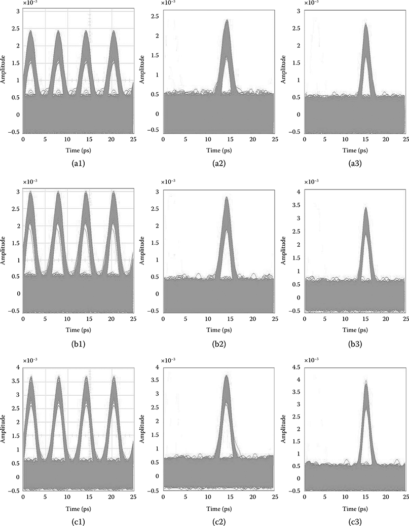
FIGURE 17.32 Eye diagrams for TOD with ranges of received power for three cases (from left to right): before demultiplexing, after demultiplexing without and with equalization.

Figure 17.33b1 through b5 shows the TOD equalization. The eye diagrams of five situations from two spans to ten spans are also distorted, since more than six spans are used in the transmission link, but these distortions are not too much, and the eye windows of these eye diagrams are still opening wide enough to have a reasonable BER. Furthermore, the FWHM of an eye when two spans are used is about 2.2 ps, while this FWHM is approximately 3 ps after transmitting through ten spans (1200 km fiber length). The received results after using an equalizer are reasonable, and there is a huge improvement as compared to signals before using the equalizer.
Further investments might be done by running simulations to count the number of errors and by calculating the BER of this transmitted system for variable transmission lengths afterward. This would give correct and exact estimations and calculations on how much the received signals could be improved by using the equalizer.

FIGURE 17.33 Eye diagrams for TOD with ranges of received power for three cases (from left to right): before demultiplexing, after demultiplexing without and with equalizer.
17.5 Concluding Remarks
Photonic signal processing based on space–time duality is very important in ultra-high-speed transmission systems. In this chapter, a foundation for the principles of temporal imaging and space–time duality have been studied and proven. From the equivalence between paraxial diffraction in space and narrow-band dispersion in time has been used to construct on analogous approximations to the relative bandwidths of spatial and temporal Fourier spectra. By using the diffraction–dispersion analogy, a quadratic phase modulation acts as a time lens, and the focal length of spatial and time lens have already been derived. The duality properties between spatial and time domains has led to temporal imaging, which would be very useful in future works, especially for designing adaptive equalizers by using phase modulation to expand or compress pulses in ultra-high-speed communication systems. Analyzing the impulse response of the temporal imaging system reveals the resolution that is related to the Fourier transform of the aperture function, and thus it proves the equivalence of the time-domain interpretation of the Fraunhofer diffraction pattern [2]. It is a very important result that solidifies the nature of the space–time duality.
With respect to photonic signal processing, a single-pulse transmission has been studied by propagating through SSMF with GVD and TOD effects without an initial chirp factor. The knowledge from the simulation results for the single pulse is then used for the design of the dispersion-compensating scheme that could eliminate not only second-order dispersion but also TOD, PMD, and timing jitter.
The space–time duality and temporal imaging are studied and then applied in the design of an adaptive equalizer system that includes a phase modulator followed by a dispersive element that could recover the initial pulse shape from distorted pulse. An efficient adaptive equalizer acts as a time lens in the time domain for optical pulse width compression by using a phase modulator, and a dispersive element is proposed, analyzed, and proven by simulation results. By using the equalizer system, the GVD effect is fully compensated. Furthermore, TOD, PMD, and timing jitter are also reduced significantly in ultra-high-speed transmission systems using a parabolic sinusoidal voltage waveform in the driving of the phase modulator. It has also been shown that an ideal parabolic phase modulation could fully recover the original pulse.
Furthermore, this adaptive equalizer has also been applied in ultra-high-speed transmission and equalization at 160 Gbps. Higher bit rates such as 320 Gbps or even higher might be possible, and would be investigated at a later stage. An evaluation of the improvement between with and without using an equalizer is also made. By monitoring the eye diagrams at the receiver end of this system, an eye of signals without an equalizer is distorted significantly, and it would return a much higher BER during transmission. On the contrary, when an adaptive equalizer is inserted, there is a critical improvement in BER as well as a wide opening eye in an eye diagram. The transmission length is increased up to 1200 km in order to investigate its limitation. We have shown the agreement between theoretical and simulation results of the performance of the equalization technique for a 160 Gbps optical transmission system under the influence of GVD, TOD, PMD impairment, and the elimination of the timing jitter, not only with a single pulse but also with 160 Gbps random sequence data transmission. The nonlinear phase shift and noises in the system might challenge the system stability.
Reference
1. G. Lifante, Integrated Photonics: Fundamentals, West Sussex: John Wiley, 2003.
2. B. H. Kolner, Space-time duality and the theory of temporal imaging, IEEE J. Quant. Electron., Vol. 30, No. 8, pp. 1951–1963, 1994.
3. C. V. Bennett and B. H. Kolner, Principles of parametric temporal imaging—Part I: System configurations, IEEE J. Quant. Electron., Vol. 36, No. 4, pp. 430–437, 2000.
4. C. V. Bennett and B. H. Kolner, Principles of parametric temporal imaging—Part II: System performance, IEEE J. Quant. Electron., Vol. 36, No. 6, pp. 649–655, 2000.
5. A. Papoulis, Systems and Transforms with Applications in Optics, New York: McGraw-Hill, 1968.
6. A. R. Adams and Y. Suematsu, Handbook of Semiconductor Lasers and Photonic Integrated Circuits, New York: Chapman and Hall, 1994.
7. G. P. Agrawal, Nonlinear Fiber Optics, 3rd ed., San Diego, CA: Academic Press, 2001.
8. T. Khayim, M. Yamauchi, D. S. Kim, and T. Kobayashi, Femtosecond optical pulse generation from a CW laser using an electro-optic phase modulator featuring lens modulation, IEEE J. Quant. Electron., Vol. 35, No. 10, pp. 1412–1418, 1999.
9. L. S. Yan, Q. Yu, T. Luo, and X. S. Yao, Compensation of higher order polarization-mode dispersion using phase modulation and polarization control in the transmitter, IEEE Photon. Technol. Lett., Vol. 14, No. 6, pp. 858–1012, 2002.
10. E. B. Treacy, Optical pulse compression with diffraction gratings, IEEE J. Quant. Electron., Vol. QE-5, pp. 454–458, 1969.
11. A. Papoulis, Pulse compression, fiber communication, and diffraction: A unified approach, J. Opt. Soc. Am. A, Vol. 11, No. 1, pp. 3–13, 1994.
12. T. Hirooka, M. Nakazawa, F. Futami, and S. Watanabe, A new adaptive equalization scheme for a 160-Gbps transmitted signal using time-domain optical Fourier transformation, IEEE Photon. Technol. Lett., Vol. 16, No. 10, pp. 2371–2373, 2004.
13. J. Azana and M. A. Muriel, Real-time optical spectrum analysis based on the time-space duality in chirped fiber gratings, IEEE J. Quant. Electron., Vol. 36, No. 5, pp. 517–526, 2000.
14. T. Jannson, Real-time Fourier transformation in dispersive optical fibers, Opt. Lett., Vol. 8, No. 4, pp. 232–234, 1983.
15. A. A. Godil, B. A. Auld, and D. M. Bloom, Picosecond time-lenses, IEEE J. Quant. Electron., Vol. 30, No. 3, pp. 827–837, 1994.
16. F. T. S. Yu and I. C. Khoo, Principles of Optical Engineering, New York: John Wiley, 1990.
17. J. W. Goodman, Introduction to Fourier Optic, New York: McGraw Hill, 1968.
18. M. T. Kauffman, A. A. Godil, B. A. Auld, W. C. Banyai, and D. M. Bloom, Applications of time lens optical systems, Electron. Lett., Vol. 29, No. 3, pp. 268–269, 1993.
19. B. H. Kolner and M. Nazarathy, Temporal imaging with a time lens, Opt. Lett., Vol. 14, No. 12, pp. 630–632, 1989.
20. B. H. Kolner and M. Nazarathy, Temporal imaging with a time lens: Erratum, Opt. Lett., Vol. 15, No. 11, p. 655, 1990.
21. C. V. Bennet, R. P. Scott, and B. H. Kolner, Temporal magnification and reversal of 100 Gbps optical data with an un-conversion time micro-scope, Appl. Phys. Lett., Vol. 65, No. 20, pp. 2513–2515, 1994.
22. T. Jannson and J. Jannson, Temporal self-imaging effect in single-mode fibers, J. Opt. Soc. Am., Vol. 71, No. 11, pp. 1373–1376, 1981.
23. B. E. A. Saleh and M. I. Irshid, Collett-Wolf equivalence theorem and propagation of a pulse in a signal mode optical fiber, Opt. Lett., Vol. 7, No. 7, pp. 342–343, 1982.
24. T. Yamamoto and M. Nakazawa, Third- and fourth-order active dispersion compensation with a phase modulator in a terabit-per-second optical time-division multiplexed transmission, Opt. Lett., Vol. 11, No. 9, pp. 647–649, 2001.
25. A. F. Elrefaie, R. E. Wagner, D. A. Atlas, and D. G. Daut, Chromatic dispersion limitations in coherent lightwave transmission systems, J. Lightwave Technol., Vol. 6, No. 5, pp. 704–709, 1988.
26. X. Li, X. Chen, and M. Qasmi, A broad-band digital filtering approach for time-domain simulation of pulse propagation in optical fiber, J. Lightwave Technol., Vol. 23, No. 2, pp. 864–875, 2005.
27. G. P. Agrawal, Fiber-Optic Communication Systems, 3rd ed., New York: John Wiley, 2002.
28. M. Romagnoli, P. Franco, R. Corsini, A. Schiffini, and M. Midrio, Time-domain Fourier optics for polarization-mode dispersion, Opt. Lett., Vol. 24, No. 17, pp. 1197–1199, 1999.
29. J. V. Howe and C. Xu, Ultrafast optical signal processing based upon space-time dualities, J. Lightwave Technol., Vol. 24, No. 7, pp. 2649–16620, 2006.
30. L. A. Jiang, M. E. Grein, H. A. Haus, E. P. Ippen, and H. Yokoyama, Timing Jitter eater for optical pulse trains, Opt. Lett., Vol. 28, pp. 78–80, 2003.
31. E. Hellstrom, H. Sunnerud, M. Westlund, and M. Karlsson, Third-order dispersion compensation using a phase modulator, J. Lightwave Technol., Vol. 21, No. 5, pp. 1188–1197, 2003.
32. M. Nakazawa, E. Yoshida, and Y. Kimura, Ultrastable harmonically and regeneratively modelocked polarization-maintaining erbium fiber ring laser, Electron. Lett., Vol. 30, pp. 1603–1604, 1994.
33. T. Hirooka and M. Nakazawa, Optical adaptive equalization of high-speed signals using time-domain optical Fourier transformation, J. Lightwave Technol., Vol. 24, No. 7, pp. 2530–2540, 2006.
34. M. Nakazawa, T. Yamamoto, and K. R. Tamura, 1.28 Tbits/s–70 km OTDM transmission using third- and fourth-order simultaneous dispersion compensation with a phase modulator, Electron. Lett., Vol. 36, No. 24, pp. 2027–2029, 2000.
35. S. Kawanishi, H. Takara, T. Morioka, O. Kamatani, K. Takiguchi, T. Kitoh, and M. Saruwatari, Single channel 400 Gbit/s time-division-multiplexed transmission of 0.98 ps pulses over 40 km employing dispersion slope compensation, Electron. Lett., Vol. 32, pp. 916–918, 1996.
36. S. Diez, R. Ludwig, and H. G. Wener, All-optical switch for TDM and WDM/TDM systems demonstrated in a 640 Gbit/s demultiplexing experiment, Electron. Lett., Vol. 34, pp. 803–805, 1998.
37. M. Daikoku, T. Miyazaki, I. Morita, H. Tanaka, F. Kubota, and M. Suzuki, 160 Gbit/s-based field transmission experiments with single polarization RZ-DPSK signals and simple PMD compensator, in European Conference on Optical Communication, 2005 (ECOC 2005), Glasgow, Scotland, September 2005, paper We2.2.1.
38. G. Lehmann, W. Schairer, H. Rohde, E. Sikora, Y. R. Zhou, A. Lord, D. Payne, et al., 160 Gbit/s OTDM transmission field trial over 550 km of legacy SSMF, in European Conference on Optical Communication 2004. (ECOC 2004), Stockholm, Sweden, September 2004, paper We1.5.2.
39. T. Hirooka, K. I. Hagiuda, T. Kumakura, K. Osawa, and M. Nakazawa, 160-Gbps–600-km OTDM transmission using time-domain optical Fourier transformation, IEEE Photon. Technol. Lett., Vol. 18, No. 24, pp. 2647–2649, 2006.