
16
Higher-Order Spectrum Coherent Receivers
This chapter presents the processing of digital signals using higher-order spectral techniques [1, 2, 3 and 4] to evaluate the performance of coherent transmission systems, especially the bispectrum method in which the signal distribution in the frequency domain is obtained in a plane. Thus, the cross-correlation as well as the signals themselves can be spatially identified. Thence, we can evaluate the impairments imposed on the transmission systems due to different causes of such degradations. Although equalization has not been described here in this chapter, the techniques for equalization using higher-order spectrum can be found in Refs. [1, 2 and 3]. The higher order will require additional processors but is compensated by additional dimensions to separate the linear and nonlinear impairments. These issues will be described in the following sections of this chapter.
16.1 Bispectrum Optical Receivers and Nonlinear Photonic Preprocessing
In this section, we present the processing of optical signals before the optoelectronic detection in the optical domain in a nonlinear optical waveguide as an nonlinear (NL) signal processing technique for digital optical receiving system for long-haul optically amplified fiber transmission systems. The algorithm implemented is a high-order spectrum (HOS) technique in which the original signals and two delayed versions are correlated via the four-wave mixing (FWM) or third harmonic conversion process. The optical receivers employing higher-order spectral photonic preprocessors and very-large-scale-integrated (VLSI) electronic systems for the electronic decoding and evaluation of the bit error rate (BER) of the transmission system are presented. A photonicsignal preprocessing system is developed to generate the triple correlation via the third harmonic conversion in a NL optical waveguide. hence the essential part of a triple correlator. The performance of an optical receiver incorporating the HOS processor is given for long-haul phase-modulated fiber transmission.
16.1.1 Introductory Remarks
As stated in previous chapters, tremendous efforts have been taken for reaching higher transmission bit rates and longer haul for optical fiber communication systems. The bit rate can reach several hundreds of Gbps and nearer to the Tbps. In this extremely high-speed operational region, the limits of electronic speed processors have been surpassed, and optical processing is assumed to play an important part of the optical receiving circuitry. Furthermore, novel processing techniques are required in order to minimize the bottlenecks of electronic processing and noises and distortion due to the impairment of the transmission medium, the linear and NL distortion effects.
This chapter deals with the photonic processing of optically modulated signals prior to the electronic receiver for long-haul optically amplified transmission systems. NL optical waveguides in planar or channel structures are studied and employed as a third harmonic converter, so as to generate a triple product of the original optical waves and its two delayed copies. The triple product is then detected by an optoelectronic receiver. Thence, the detected current would be electronically sampled and digitally processed to obtain the bispectrum of the data sequence, and a recovery algorithm is used to recover the data sequence. The generic structures of such high-order spectral optical receivers are shown in Figure 16.1. For the nonlinear photonic processor (Figure 16.1a), the optical signals at the input are delayed and then coupled to a nonlinear photonic device in which the nonlinear conversion process is implemented through the use of third harmonic conversion or degenerate FWM. In the nonlinear digital processor (see Figure 16.1b), the optical signals are detected coherently and then sampled and processed using the nonlinear triple correlation and decoding algorithm.
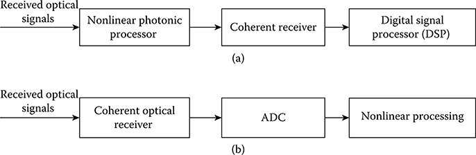
FIGURE 16.1 Generic structure of high-order spectrum optical receiver; (a) photonic preprocessor and (b) nonlinear DSP-based coherent receiver. Note that both in-phase and quadrature components can be processed as combined signals.
We propose and simulate this NL photonic preprocessor optical receiver under the MATLAB® and Simulink® platform for differentially coded phase shift keying, the DQPSK modulation scheme.
This section is organized as follows: Section 16.1.3 gives a brief introduction of the triple correlation and bispectrum processing techniques. Section 16.1.4 introduces the simulation platform for the long-haul optically amplified optical fiber communication systems. Section 16.2.2.1 then gives the implementation of the NL optical processor which consists of a nonlinear optical waveguide and an optical receiver associated with a digital signal processing (DSP) sub-systems operating in the electronic domain, so as to recover the data sequence. The performance of the transmission system is given with an evaluation of the BER under linear and NL transmission regimes.
16.1.2 Bispectrum
In signal processing, the power spectrum estimation showing the distribution of power in the frequency domain is a useful and popular tool to analyze or characterize a signal or process. However, the phase information between frequency components is suppressed in the power spectrum. Therefore, it is necessarily useful to exploit higher-order spectra known as multidimensional spectra instead of the power spectrum in some cases, especially in nonlinear processes or systems [5]. Different from the power spectrum, the Fourier transform of the autocorrelation, multidimensional spectra are known as Fourier transforms of high-order correlation functions, and hence they provide us not only the magnitude information but also the phase information.
In particular, the two-dimensional spectrum, also called bispectrum, is by definition the Fourier transform of the triple correlation or the third-order statistics [2]. For a signal x(t), its triple correlation function C3 is defined as
where τ1, τ2 are the time-delay variables. Thus, the bispectrum can be estimated through the Fourier transform of C3 as follows
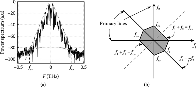
FIGURE 16.2 A description of (a) power spectrum regions and (b) bispectrum regions for explanation.
where F{} is the Fourier transform, and f1, f2 are the frequency variables. From the definitions of Equations 16.1 and 16.2, both the triple correlation and the bispectrum are represented in a 3D graph with two variables of time and frequency, respectively. Figure 16.2 shows the regions of the power spectrum and bispectrum, respectively, and their relationship. The cutoff frequencies are determined by intersection between the noise and spectral lines of the signal. These frequencies also determine the distinct areas that are basically bounded by a hexagon in a bispectrum. The area inside the hexagon only shows the relationship between frequency components of the signal, whereas the area outside shows the relationship between the signal components and noise. Due to the two-dimensional representation in bispectrum, the variation of the signal and the interaction between signal components can easily be identified.
Because of the unique features of the bispectrum, it is really useful in characterizing the non-Gaussian or nonlinear processes and applicable in various fields such as signal processing [1,2], biomedicine, and image reconstruction. The extension of a number of representation dimensions makes the bispectrum become more easily and significantly a representation of different types of signals and differentiation of various processes, especially nonlinear processes such as doubling and chaos. Hence, the multidimensional spectra technique is proposed as a useful tool to analyze the behaviors of signals generated from these systems.
16.1.3 Bispectrum Coherent Optical Receiver
Figure 16.1 shows the structure of a bispectrum optical receiver in which there are three main sections: an all-optical preprocessor, an optoelectronic detection, and amplification including an analog-to-digital converter (ADC) to generate sampled values of the triple-correlated product. This section is organized as follows. The next subsection gives an introduction to bispectrum and associate noise elimination as well as the benefits of the bispectrum techniques, then the details of the bispectrum processor are given, and then some implementation aspects of the bispectrum processor using VLSI are stated.
16.1.4 Triple Correlation and Bispectra
16.1.4.1 Definition
The power spectrum is the Fourier transform of the autocorrelation of a signal. The bispectrum is the Fourier transform of the triple correlation of a signal. Thus, both the phase and amplitude information of the signals are embedded in the triple-correlated product.
While autocorrelation and its frequency-domain power spectrum do not contain the phase information of a signal, the triple correlation contains both, due to the definition of triple correlation,
where S(t) is the continuous time-domain signal to be recovered, and τ1, τ2 are the delay time intervals. For the special cases where τ1 = 0 or τ2 = 0, the triple correlation is proportional to the autocorrelation. It means that the amplitude information is also contained in the triple correlation. The benefit of holding phase and amplitude information is that it gives a potential to recover the signal back from its triple correlation. In practice, the delays τ1 and τ2 indicate the path difference between the three optical waveguides. These delay times are corresponding to the frequency regions in the spectral domain. Thus, different time intervals would determine the frequency lines in the bispectrum.
16.1.4.2 Gaussian Noise Rejection
Let S(n) be a deterministic sampled signal which the sampled version of the continuous signals S(t). S(n) is corrupted by Gaussian noise w(n), where n is the sampled time index. The observed signal takes the form Y(n) = S(n) + w(n). The polyspectra of any Gaussian process is zero for any order greater than two [2]. The bispectrum is the third-order polyspectrum and offers significant advantage for signal processing over the second-order polyspectrum, commonly known as the power spectrum, which is corrupted by Gaussian noise. Theoretically speaking, the bispectral analysis allows us to extract a non-Gaussian signal from the corrupting effects of Gaussian noise.
Thus, for a signal that has arrived at the optical receiver, the steps to recover the amplitude and phase of the lightwave-modulated signals are as follows:
Estimating the bispectrum of S(n) based on observations of Y(n).
From the amplitude and phase bispectra, form an estimate of the amplitude and phase distribution in one-dimensional frequency of the Fourier transform of S(n). These form the constituents of the signal S(n) in the frequency domain.
Thence, taking the inverse Fourier transform to recover the original signal S(n). This type of receiver can be termed as the bispectral optical receiver.
16.1.4.3 Encoding of Phase Information
The bispectra contains almost complete information about the original signal (magnitude and phase). And thus, if the original signal x(n) is real and finite, it can be reconstructed, except for a shift a. Equivalently, the Fourier transform can be determined, except for a linear shift factor of e−j2πωa. By determining two adjacent pulses, any differential phase information will then be readily available [5]. In other words, the bispectra, and hence the triple correlation, contain the phase information of the original signal, allowing it to “pass through” the square law photodiode, which would otherwise destroy this information. The encoded phase information can then be recovered up to a linear phase term, thus necessitating a differential coding scheme.
16.1.4.4 Eliminating Gaussian Noise
For processes that have zero mean and the symmetrical probability density function (PDF), their third-order cumulants are equal to zero. Therefore, in a triple correlation, those symmetrical processes are eliminated. Gaussian noise is assumed to affect the signal quality. Mathematically, the third cumulant is defined as where mk is the k-th order moment of the signal, especially since it is the mean of the signal. Thus, for the zero mean and symmetrical PDF, its third-order cumulant becomes zero [1,2]. Theoretically, considering the signal as u(t) = s(t) + n(t), where n(t) is an additive Gaussian noise, the triple correlation of u(t) will reject Gaussian noise affecting the s(t).
16.1.5 Transmission and Detection
16.1.5.1 Optical Transmission Route and Simulation Platform
Shown in Figure 16.3 is the schematic of the transmission link over a total length of 700 km, with sections from Melbourne city (in Victoria, Australia) to Gippsland, the inland section in Victoria (city to coastal landing for submarine connection), thence an undersea section of more than 300 km crossing the Bass Strait to George Town of Tasmania (undersea or submarine), and then inland transmission to Hobart of Tasmania (coastal area to city connection). The Gippsland/George Town link is shown in Figure 16.3. Other inland sections in Victoria and Tasmania of Australia are structured with optical fibers and lumped optical amplifiers (Er-doped fiber amplifiers—EDFA). Raman distributed optical amplification (ROA) is used by pump sources located at both ends of the Melbourne-to-Hobart link, including the 300 km undersea section. The undersea section of nearly 300 km long of fibers consisting of only the transmission and dispersion-compensating sections, no active subsystems are included. Only Raman amplification is used with the pump sources injecting the laser beams into both sides of the section. These pump sources are located on the shores of the inland area. This 300 km distance is a fairly long one, and only Raman distributed gain is used. Simulink models of the transmission system including the optical transmitter, the transmission line, and the bispectrum optical receiver are given.
16.1.5.2 FWM and Bispectrum Receiving
We have also integrated the waveguide whose material parameters are real into the MATLAB and Simulink of the transmission system so that the NL parametric conversion system is very close to practice. The spectra of the optical signals before and after this amplification are shown in Figure 16.4, indicating the conversion efficiency. This indicates the performance of the bispectrum optical receiver (Figures 16.5 and 16.6).
16.1.5.3 Performance
We implement the models for both techniques for binary phase shift keying modulation format for serving as a guideline for phase modulation optical transmission systems using nonlinear preprocessing. We note the following:
The arbitrary white Gaussian noise (AWGN) block in the Simulink platform can be set in different operating modes. This block then accepts the signal input and assumes the sampling rate of the input signal, then estimates the noise variance based on Gaussian distribution and the specified signal-to-noise ratio (SNR). This is then superimposed on the amplitude of the sampled value. Thus, we believe, at that stage, that the noise is contributed evenly across the entire band of the sampled time (converted to spectral band).
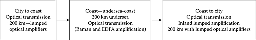
FIGURE 16.3 Schematic of the transmission link including inland and undersea sections between city and coast (inland beach), then undersea and coast (inland) to city.
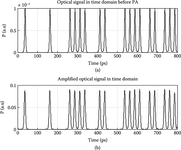
FIGURE 16.4 Time traces of the optical signal: (a) before and (b) after the parametric amplifier.
The ideal curve SNR versus the BER plotted in the graph provided is calculated using the commonly used formula in several textbooks on communication theory. This is evaluated based on the geometrical distribution of the phase states, and then the noise distribution over those states. This means that all the modulations and demodulations are assumed to be perfect. However, in digital system simulation, the signals must be sampled. This is even more complicated when a carrier is embedded in the signal, especially when the phase shift keying (PSK) modulation format is used.
We thus re-setup the models of (i) AWGN in a complete binary phase shift keying (BPSK) modulation format with both the ideal coherent modulator and demodulator and any necessary filtering required, (ii) AWGN blocks with the coherent modulator and demodulator incorporating the triple correlator and necessary signal processing block. This is done in order to make fair comparison between the two pressing systems.
In our former model, the AWGN block was being used incorrectly, in that it was being used in “SNR” mode, which applies the noise power over the entire bandwidth of the channel, which of course is larger than the data bandwidth, meaning that the amount of noise in the data band was a fraction of the total noise applied. We accept that this was an unfair comparison to the theoretical curve that is given against Eb/N0, as defined in Ref. [1].
In the current model, we provide a fair comparison noise that was added to the modulated signal using the AWGN block in the Eb/N0 mode (E0 is the energy per bit and N0 is the noise contained within the bit period), with the “symbol period” set to the carrier period, and, in effect, this set the “carrier-to-noise” ratio, or CNR. Also, the triple correlation receiver was modified a little from the original, namely the addition of the BP filter and some tweaking of the triple correlation delays, which resulted in the BER curve shown in Figure 16.7. Also, an ideal homodyne receiver model was constructed with the noise added and measured in the exact same method as the triple correlation model. This provided a benchmark to compare the triple correlation receiver against.
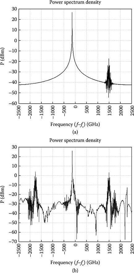
FIGURE 16.5 Corresponding spectra of the optical signal: (a) before and (b) after the parametric amplifier.
Furthermore, we can compare the simulated BER values with the theoretical limit set by
by relating the CNR to Eb/N0 as in the following,
where the channel bandwidth BW is 1600 Hz, set by the sampling rate, and fs is the symbol rate—in our case, a symbol is one carrier period (100 Hz), as we are adding noise to the carrier. These frequencies are set at the normalized level, so as to scale to wherever spectral regions would be of interest. As can be seen in Figure 16.7, the triple correlation receiver matches the performance of the ideal homodyne case and closely approaches the theoretical limit of BPSK (approximately 3 dB at a BER of 10−10). As discussed, the principle benefit from the triple correlation over the ideal homodyne case will be the characterization of the noise of the channel that is achieved by analysis of the regions of symmetry in the 2D bispectrum. Finally, we still expect possible performance improvement when symbol identification is performed directly from the triple correlation matrix, as opposed to the traditional method that involves recovering the pulse shape first. It is not possible at this stage to model the effect of the direct method.
FIGURE 16.6 (a) Input data sequence and (b) detected sequence processed using triple correlation nonlinear photonic processing and recovery scheme bispectrum receiver.
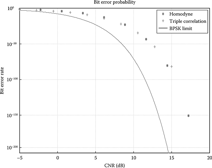
FIGURE 16.7 BER versus carrier/noise ratio in power for nonlinear triple correlation, ideal BPSK under homodyne coherent detection, and ideal BPSK limit. Note that, in practice, the BER of up to 1e−19 would be the lowest value used.
Equalization of digital sampled signals can be implemented by employing the algorithms described in Ref. [1].
16.2 Nonlinear Photonic Signal Processing Using Higher-Order Spectra
16.2.1 Introductory Remarks
With the increasing demand for high capacity, communication networks are facing several challenges, especially in signal processing at the physical layer at ultra-high speeds. When the processing speed is over that of the electronic limit or requires massive parallel and high-speed operations, the processing in the optical domain offers significant advantages. Thus, all-optical signal processing is a promising technology for future optical communication networks. An advanced optical network requires a variety of signal processing functions, including optical regeneration, wavelength conversion, optical switching, and signal monitoring. An attractive way to realize these processing functions in transparent and high-speed modes is to exploit the third-order nonlinearity in optical waveguides, particularly parametric processes.
Nonlinearity is a fundamental property of optical waveguides, including channel, rib-integrated structures, or circular fibers. The origin of nonlinearity comes from the third-order nonlinear polarization in optical transmission media. It is responsible for various phenomena such as self-phase modulation (SPM), cross-phase modulation (XPM), and FWM effects. In these effects, the parametric FWM process is of special interest, because it offers several possibilities for signal processing applications. To implement all-optical signal processing functions, highly nonlinear optical waveguides are required where the field of the guided waves is concentrated in its core region. Hence we must use a guided medium whose nonlinear coefficient is sufficiently high so as to achieve the required energy conversion. Therefore, the highly nonlinear fibers (HNLFs) are commonly employed for this purpose, since the nonlinear coefficient of HNLF is about tenfold higher than that of standard transmission fibers. Indeed, the third-order nonlinearity of conventional fibers is often very small to prevent the degradation of the transmission signal from nonlinear distortions. Recently, nonlinear chalcogenide and tellurite glass waveguides have emerged as a promising device for ultra-high-speed photonic processing. Because of their geometries, these waveguides are called planar waveguides. A planar waveguide can confine the lightwaves within an area comparable to the effective wavelength of lighwaves in the medium. Hence, they are very compact for signal processing.
16.2.2 FWM and Photonic Processing for Higher-Order Spectra
16.2.2.1 Bispectral Optical Structures
Figure 16.8 shows the generic and detailed structure of the bispectral optical receiver, respectively, which consists of (1) an all-optical preprocessor front end, followed by (2) a photodetector and electronic amplifier to transfer the detected electronic current to a voltage level appropriate for sampling by an ADC and thus the signals at this stage is in sampled form; (3) the sampled triple correlation product is then transformed to the Fourier domain using the FFT. The product at this stage is the row of the matrix of the bispectral amplitude and phase plane (see Figure 16.10). A number of parallel structures may be required if passive delay paths are used; (4) a recovery algorithm is used to derive the one-dimensional distribution of the amplitude and phase as a function of the frequency, which are the essential parameters required for taking the inverse Fourier transform to recover the time-domain signals.
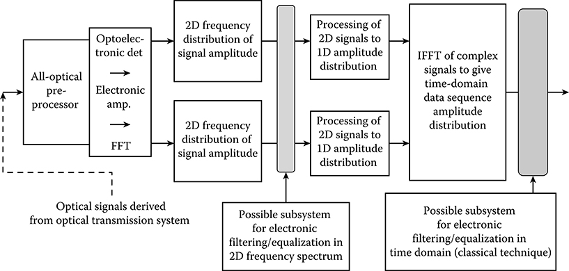
FIGURE 16.8 Generic structure of an optical preprocessing receiver employing bispectrum processing technique.
The physical process of mixing the three waves to generate the fourth wave whose amplitude and phase are proportional to the product of the three input waves is well known in literature of NL optics. This process requires (1) a highly NL medium so as to efficiently convert the energy of the three waves to that of the fourth wave and (2) satisfying the phase-matching conditions of the three input waves of the same frequency (wavelength) to satisfy the conservation of momentum.
16.2.2.2 Phenomena of FWM
The origin of the FWM comes from the parametric processes that lie in the NL responses of bound electrons of a material to applied optical fields. More specifically, the polarization induced in the medium is not linear in the applied field, but contains NL terms whose magnitude is governed by the NL susceptibilities [3,4,6]. The first-, second-, and third-order parametric processes can occur due to these NL susceptibilities [χ1 χ2 χ3]. The coefficient χ3 is responsible for the FWM that is exploited in this work. Simultaneously with this FWM, there is also a possibility of the generation of third harmonic waves by mixing the three waves and using parametric amplification. The third harmonic generation is normally very small, due to the phase mismatching of the guided wave number (the momentum vector) between the fundamental waves and the third harmonic wave. FWM in guided wave medium such as single-mode optical fibers have been extensively studied due to its efficient mixing to create the fourth wave [4]. The exploitation of the FWM processes in channel optical waveguides has not yet been extensively exploited. In this chapter, we demonstrate theoretical and experimentally the applications of such process in enhancing the sensitivity of the receiver by nonlinear processes.
The three lightwaves are mixed to generate the polarization vector due to the NL third-order susceptibility, given as
where ε0 is the permittivity in vacuum; are the electric field components of the lightwaves; is the total field entering the NL waveguide; and χ(3) is the third-order susceptibility of the NL medium. PNL is the product of the three total optical fields of the three optical waves here that gives the triple product of the waves required for the bispectrum receiver, in which the NL waveguide acts as a multiplier of the three waves that are considered as the pump waves in this section. The mathematical analysis of the coupling equations via the wave equation is complicated, but straightforward. Let ω1, ω2, ω3, and ω4 be the angular frequencies of the four waves of the FWM process, linearly polarized along the horizontal direction y of the channel waveguides and propagating along the z-direction. The total electric field vector of the four waves is given by
with = unit vector along y axis, and_c.c. = complex conjugate.
The propagation constant can be obtained by , where neff,i is the effective index of the i-th guided waves Ei(i = 1,...,4), which can be either transverse electric (TE) or transverse magnetic (TM) polarized guided mode propagating along the channel NL optical waveguide, and all four waves are assumed to be propagating along the same direction. Substituting Equation 16.8 in Equation 16.7, we obtain
where Pi(i = 1,...,4) consists of a large number of terms involving the product of three electric fields of the optical-guided waves, for example, the term P4 can be expressed as
with
The first four terms of Equation 16.10 represent the SPM and XPM effects, which are dependent on the intensity of the waves. The remaining terms result in FWM. Thus, the question is, which terms are the most effective components that resulted from the parametric mixing process? The effectiveness of the parametric coupling depends on the phase-matching terms governed by φ+ and φ−, or a similar quantity.
It is obvious that significant FWM would occur if the phase matching is satisfied. This requires the matching of both the frequency as well as the wave vectors, as given in Equation 16.10. From Equation 16.10, we can see that the term φ+ corresponds to the case in which three waves are mixed to give the fourth wave whose frequency is three times that of the original wave—this is the third harmonic generation. However, normally the matching of the wave vectors would not be satisfied due to the dispersion effect or the differential mismatching of the wave momentum vectors as guided in a channel optical waveguide. If there is a large mismatching of the momentum vectors of the fundamental and third-order harmonics then only a minute amount of energy would be transferred to the third harmonic components.
The conservation of momentum derived from the wave vectors of the four waves requires that
The effective refractive indices of the guided modes of the three waves E1, E2, and E3 are the same, as are their frequencies. This condition is automatically satisfied, provided that the NL waveguide is designed such that it supports only a single polarized-mode, TE or TM, and with minimum dispersion difference within the band of the signals.
16.2.3 Third-Order Nonlinearity and Parametric FWM Process
16.2.3.1 Nonlinear Wave Equation
In optical waveguides, including optical fibers, the third-order nonlinearity is of special importance because it is responsible for all nonlinear effects. The confinement of lightwaves and their propagation in optical waveguides are generally governed by the nonlinear wave equation (NLE), which can be derived from the Maxwell’s equations under the coupling of nonlinear polarization. The nonlinear wave propagation in nonlinear waveguide in the time-spatial domain in vector form can be expressed as (see also Chapter 2)
where is the electric field vector of the lightwave, μ0 is the vacuum permeability assuming a nonmagnetic waveguiding medium, c is the speed of light in vacuum, and are, respectively, the linear and nonlinear polarization vectors, which are formed as
where χ(3) is the third-order susceptibility. Thus, the linear and nonlinear coupling effects in optical waveguides can be described by Equation 16.12. The second term on the right-hand side is responsible for nonlinear processes including interaction between optical waves through third-order susceptibility.
In most telecommunication applications, only complex envelopes of optical signals is considered in analysis because the bandwidth of the optical signal is much smaller than the optical carrier frequency. To model the evolution of the light propagation in optical waveguides, it requires that Equation 16.12 be further modified and simplified by some assumptions that are valid in most telecommunication applications. Hence, the electrical field can be written as
where A(z,t) is the slowly varying complex envelope propagating along z in the waveguide, and k is the wave number. After some algebra using the method of separating variables, the following equation for propagation in optical waveguide is obtained [7]
where the effect of propagation constant β around ω0 is Taylor-series expanded, and g(t) is the nonlinear response function including the electronic and nuclear contributions. For the optical pulses wide enough to contain many optical cycles, Equation 16.15 can be simplified as
where a frame of reference moving with the pulse at the group velocity vg is used by making the transformation τ t − z/vg ≡ t − β1z , and A is the total complex envelope of propagation waves; α, βk are the linear loss and dispersion coefficients, respectively; γ = ω0 n2/cAeff is the nonlinear coefficient of the guided wave structure; and the first moment of the nonlinear response function is defined as
Equation 16.17 is the basic propagation equation, commonly known as the nonlinear Schrödinger equation (NLSE), which is very useful for investigating the evolution of the amplitude of the optical signal and the phase of the lightwave carrier under the effect of third-order nonlinearity in optical waveguides. The left-hand side (LHS) in Equation 16.17 contains all linear terms, while all nonlinear terms are contained on the right-hand side. In this equation, the first term on the right-hand side is responsible for the intensity-dependent refractive index effects, including FWM.
16.2.3.2 FWM Coupled-Wave Equations
FWM is a parametric process through the third-order susceptibility χ(3). In the FWM process, the superposition and generation of the propagating of the waves with different amplitudes Ak, frequencies ωk, and wave numbers kk through the waveguide can be represented as
By ignoring the linear and scattering effects and with the introduction of Equation 16.19 in Equation 16.17, the NLSE can be separated into coupled differential equations, each of which is responsible for one distinct wave in the waveguide
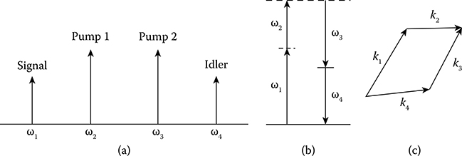
FIGURE 16.9 (a) Position and notation of the distinct waves, (b) diagram of energy conservation, and (c) diagram of momentum conservation in FWM.
where Δk = k1 + k2 − k3 − k4 is the wave vector mismatch. The equation system (Equation 16.20) thus describes the interaction between different waves in nonlinear waveguides. The interaction that is represented by the last term in Equation 16.20 can generate new waves. For three waves with different frequencies, a fourth wave can be generated at frequency ω4 = ω1 + ω2 − ω3. The waves at frequencies ω1 and ω2 are called pump waves, whereas the wave at frequency ω3 is the signal, and the generated wave at ω4 is called the idler wave, as shown in Figure 16.9a. If all three waves have the same frequency ω1 = ω2 = ω3, the interaction is called a degenerate FWM with the new wave at the same frequency. If only two of the three waves are at the same frequency (ω1 = ω2 ≠ ω3), the process is called partly degenerate FWM, which is important for some applications such as the wavelength converter and parametric amplifier.
16.2.3.3 Phase Matching
In parametric nonlinear processes such as FWM, the energy conservation and momentum conservation must be satisfied to obtain a high efficiency of the energy transfer, as shown in Figure 16.9a. The phase-matching condition for the new wave requires
During propagation in optical waveguides, the relative phase difference θ(z) between the four involved waves is determined by
where φk(z) relates to the initial phase and the nonlinear phase shift during propagation. An approximation of phase-matching condition can be given as
where Pk is the power of the waves, and κ is the phase mismatch parameter. Thus, the FWM process has maximum efficiency for κ = 0. The mismatch comes from the frequency dependence of the refractive index and the dispersion of optical waveguides. Depending on the dispersion profile of the nonlinear waveguides, it is very important in the selection of pump wavelengths to ensure that the phase mismatch parameter is minimized.
Once the fourth wave is generated, the interaction of the four waves along the section of the waveguide continues to happen, and thus the NL Schrödinger equation must be used to investigate the evolution of the waves.
16.2.3.4 Coupled Equations and Conversion Efficiency
To derive the wave equations to represent the propagation of the three waves to generate the fourth wave, we can resort to Maxwell’s equations. It is lengthy to write down all the steps involved in this derivation, so we summarize the standard steps usually employed to derive the wave equations as follows: First, add the NL polarization vector given in Equation 16.7 into the electric field density vector D. Then, taking the curl of the first Maxwell’s equation and using the second equation of the four Maxwell’s equations and substituting the electric field density vector and using the fourth equation, one would then come up with the vectorial wave equation.
For the FWM process occurring during the interaction of the three waves along the propagation direction of the NL optical channel waveguide, the evolution of the amplitudes, A1–A4, of the four waves, E1–E4, given in Equation 16.20, is given by (only the A1 term is given)
where the wave vector mismatch Δk is given in Equation 16.11, and the * denotes the complex conjugation. Note that the coefficient n2 in Equation 16.24 is defined as the nonlinear coefficient which is related to the nonlinear susceptibility of the medium. This coefficient can be defined as
16.2.4 Optical Domain Implementation
16.2.4.1 Nonlinear Wave Guide
In order to satisfy the condition of FWM and efficient energy transfer between the waves, a guided medium is preferred, thus a rib-waveguide can be employed for guiding. In this case a glass material of AS2S3 or TeO2 whose NL refractive index coefficient is about 100,000 times greater than that of silica is produced for forming the nonlinear waveguide. The three waves are guided in this waveguide structure. Their optical fields are overlapped. The cross-section of the waveguide is in the order of 4 × 0.4 μm. The waveguide cross-section can be designed such that the dispersion is “flat” over the spectral range of the input waves, ideally from 1520 nm to 1565 nm. This can be done by adjusting the thickness of the rib structure.
The fourth wave generated from the FWM waveguide is then detected by the photodetector, which acts as an integrating device. Thus, the output of this detector is the triple correlation product in the electronic domain that we are looking for.
If equalization or filtering is required, then these functional blocks can be implemented in the bispectral domain as shown in Figure 16.8. Figure 16.10 shows the parallel structures of the bispectral receiver so as to obtain all rows of the bispectral matrix. The components of the structure are almost similar, except the delay time of the optical preprocessor.
In the NL channel waveguide, fabricated using TeO2 (tellurium oxide) on silica, the interaction of the three waves, one original and two delayed beams, happens via the electronic processes, with highly NL coefficient [χ3] converting to the fourth wave.
When the three waves are co-propagating, due to the conservation of the momentum of the interaction and exchange of energy of the four waves the fourth wave is produced that satisfy the FWM phase matching conditions. Indeed, phase matching can also be satisfied by one forward wave and two backward-propagating waves (delayed version of the first wave), leading to almost 100% conversion efficiency to generate the fourth wave.
FIGURE 16.10 Parallel structures of photonic preprocessing to generate a triple correlation product in the optical domain.
The interaction of the three waves via the electronic process and the χ(3) gives rise to the polarization vector P, which in turn couples with the electric field density of the lightwaves and then with the NL Schrödinger wave equation. By solving and modeling this wave equation with the FWM term on the right-hand side of the equation, one can obtain the wave output (the fourth wave) at the end of the NL waveguide section.
16.2.4.2 Third Harmonic Conversion
Third harmonic conversion may happen, but at extremely low efficiencies, at least 1000 times less than that of FWM due to the nonmatching of the effective refractive indices of the guided modes at 1550 nm (fundamental wave) and 517 nm (third harmonic wave).
It is noted that the common term for this process is the matching of the dispersion characteristics, that is, k/omega, where omega is the radial frequency of the waves at 1550 and 1517 nm, versus the thickness of the waveguide.
16.2.4.3 Conservation of Momentum
The conservation of momentum and, thus, phase-matching condition for the FWM are satisfied without much difficulty, as the wavelengths of the three input waves are the same direction. Thus it requires that the generated waves propagating in the guide must satisfy this condition. Thence the optical NL channel waveguide must be designed such that there is no mismatching of the third harmonic conversion and the other forward and backward waves. It is considered that single polarized mode, either TE or TM, will be used to achieve efficient FWM. Thus, the dimension of the channel waveguide would be estimated at about 0.4 μm (height) × 4 μm (width).
16.2.4.4 Estimate of Optical Power Required for FWM
In order to achieve efficient FWM conversion, the NL coefficient n2 must be large. This coeffcient is proportional to χ(3) by a constant 8n/3, with n as the effective refractive index. This NL coefficient is then multiplied by the intensity of the guided waves to give an estimate of the phase change and, thence, estimation of the efficiency of the FWM. The cross-section of the waveguide can be estimated by using Equation 16.3. Due to high index difference between the waveguide and its cladding, the guided mode is well confined. Hence the effective area of the guided waves is very close to the cross-section area. Thus, an average power of the guided waves would be about 3–5 mW, or about 6 dBm.
The loss of the linear section which is section of multimode interference and delay split is estimated at 3 dB. Thus, the input power of the three waves required for efficient FWM is about 10 dBm (maximum).
16.2.5 Transmission Models and Nonlinear Guided Wave Devices
To model the parametric FWM process between multiwaves, the basic propagation equations described in Section 16.2.3 are used. There are two approaches to simulate the interaction between waves. The first approach, named as the separating channel technique, is to use the coupled equations system (Equation 16.20) in which the interactions between different waves are obviously modeled by certain coupling terms in each coupled equation. Thus, each optical wave considered as one separated channel is represented by a phasor. The coupled equations system is then solved to obtain the solutions of the FWM process. The outputs of the nonlinear waveguide are also represented by separated phasors, and hence the desired signal can be extracted without using a filter (Figure 16.11).
The second or alternative approach is to use the propagation equation (Equation 16.17), which allows us to simulate all evolutionary effects of the optical waves in the nonlinear waveguides. In this technique, a total field is used instead of individual waves. The superimposed complex envelope A is represented by only one phasor, which is the summation of individual complex amplitudes of different waves, given as
where ω0 is the defined angular central frequency, and An, ωn are the complex envelope and carrier frequency of individual waves, respectively. Hence, various waves at different frequencies are combined into a total signal vector, which facilitates integration of the nonlinear waveguide model into the Simulink platform. Equation 16.17 can also be numerically solved by the split-step Fourier method (SSFM). The Simulink block, representing the nonlinear waveguide, is implemented with an embedded MATLAB program. Because only complex envelopes of the guided waves are considered in the simulation, each of the different optical waves is shifted by a frequency difference between the central frequency and the frequency of the wave to allocate the wave in the frequency band of the total field. Then, the summation of the individual waves, which is equivalent to the combination process at the optical coupler, is performed prior to entering the block of nonlinear waveguide, as depicted in Figure 16.12. The output of the nonlinear waveguide will be selected by an optical bandpass filter (BPF). In this way, the model of nonlinear waveguide can be easily connected to other Simulink blocks that are available in the platform for simulation of optical fiber communication systems.
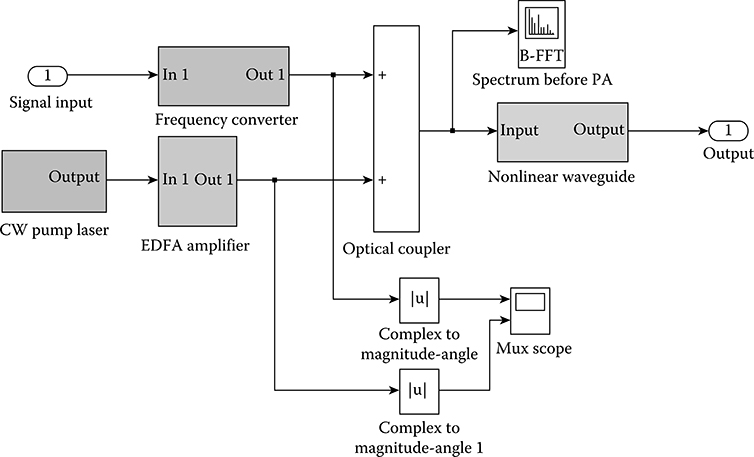
FIGURE 16.11 Typical Simulink® setup of the parametric amplifier using the model of nonlinear waveguide.
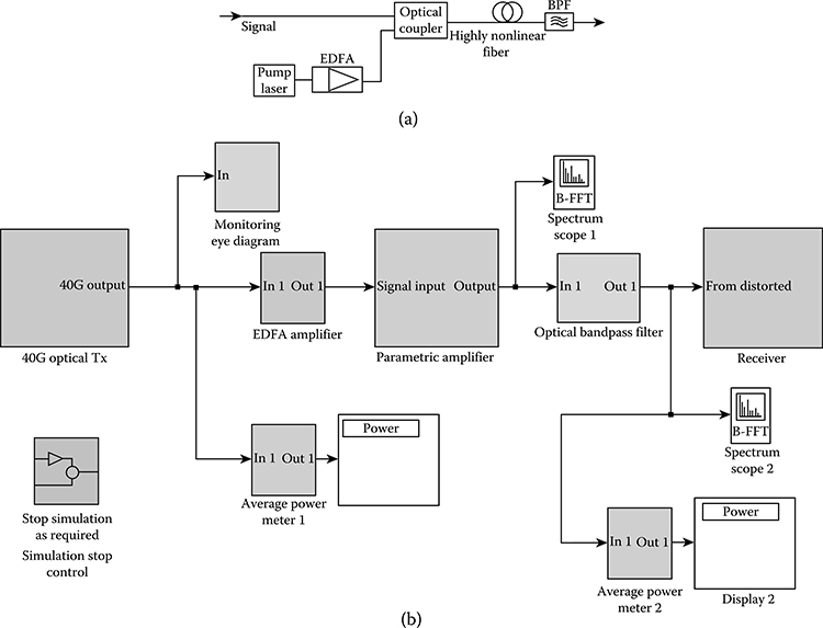
FIGURE 16.12 (a) The typical setup of an optical parametric amplifier and (b) Simulink® model of optical parametric amplifier.
16.3 System Applications of Third-Order Parametric Nonlinearity in Optical Signal Processing
In this section, a range of signal processing applications are demonstrated through simulations that use the model of nonlinear waveguide to model the wave mixing process.
16.3.1 Parametric Amplifiers
One of the important applications of the χ(3) nonlinearity is parametric amplification. The optical parametric amplifiers (OPA) offer a wide gain bandwidth, high differential gain, and optional wavelength conversion and operation at any wavelength [7]. These important features of OPA are obtained because the parametric gain process do not rely on energy transitions between energy states, but it is based on highly efficient FWM in which two photons at one or two pump wavelengths interact with a signal photon. The fourth photon, the idler, is formed with a phase such that the phase difference between the pump photons and the signal and idler photons satisfies the phase-matching condition (Equation 16.21). The schematic of the fiber-based parametric amplifier is shown in Figure 16.12a. The parameters of the OPA are given in Table 16.1.
TABLE 16.1
Critical Parameters of the Parametric Amplifier in a 40 Gbps System
For parametric amplifier using one pump source, from the coupled equations (Equation 16.20) with A1= A2 = Ap, A3 = As, and A4 = Ai, it is possible to derive three coupled equations for complex field amplitudes of the three waves Ap,s,i
The analytical solution of these coupled equations determines the gain of the amplifier [4].
with L is the length of the highly nonlinear fiber/waveguide, Pp is the pump power, and g is the parametric gain coefficient
where the phase mismatch Δk can be approximated by extending the propagation constant in a Taylor series around ω0
Here, dD/dλ is the slope of the dispersion factor D(λ) evaluated at the zero dispersion of the guided wave component, that is, at the optical wavelength, λk = 2πc/ωk.
FIGURE 16.13 Time traces of the 40 Gbps signal (a) before and (b) after the parametric amplifier.
Figure 16.13b shows the Simulink setup of the 40 Gbps RZ transmission system using a parametric amplifier. The setup contains a 40 Gbps optical RZ transmitter, an optical receiver for monitoring, a parametric amplifier block, and a BPF that filters the desired signal from the total field output of the amplifier. Details of the parametric amplifier block can be seen in Figure 16.12. The block setup of the parametric amplifier consists of a continuous wave (CW) pump laser source, an optical coupler to combine the signal and the pump, and a highly nonlinear fiber block that contains the embedded MATLAB model for nonlinear propagation. The important simulation parameters of the system are listed in Table 16.2.
Figure 16.14 shows the signals before and after the amplifier in the time domain. The time trace indicates the amplitude fluctuation of the amplified signal as a noisy source from a wave mixing process. Their corresponding spectra are shown in Figure 16.15. The noise floor of the output spectrum of the amplifier shows the gain profile of OPA. Simulated dependence of OPA gain on the wavelength difference between the signal and the pump as shown in Figure 16.16, together with theoretical gain using Equation 16.15. The plot shows an agreement between theoretical and simulated results. The peak gain is achieved at phase-matched conditions where the linear phase mismatch is compensated for by the nonlinear phase shift.
16.3.1.1 Wavelength Conversion and Nonlinear Phase Conjugation
Beside the signal amplification in a parametric amplifier, the idler is generated after the wave mixing process. Therefore, this process can also be applied to wavelength conversion. Due to the very fast response of the third-order nonlinearity in optical waveguides, the wavelength conversion based on this effect is transparent to the modulation format and the bit rate of signals. For a flat wideband converter, which is a key device in wavelength-division multiplexing (WDM) networks, a short-length HNLF with a low dispersion slope is required in design. By a suitable selection of the pump wavelength, the wavelength converter can be optimized to obtain a bandwidth of 200 nm. Therefore, the wavelength conversion between bands such as C and L bands can be performed in WDM networks. Figure 16.16 shows an example of the wavelength conversion for four WDM channels at the C band. The important parameters of the wavelength converter are shown in Table 16.2. The WDM signals are converted into the L-band with a conversion efficiency of −12 dB.
TABLE 16.2
Critical Parameters of the Parametric Amplifier in a 40 Gbps Transmission System
RZ 40 Gbps Signal |
| λ0 = 1559 nm, λs = {1531.12, 1537.4, 1543.73, 1550.12} nm, Ps = 1 mW (peak), Br = 40 Gbps |
Parametric Amplifier |
| L pump source: Pp = 100 mW (after EDFA), λp = 1560.07 nm |
| HNLF: Lf = 200 m, D = 0.02 ps/km/nm, S = 0.03 ps/nm2/km, α = 0.5 dB/km, Aeff = 12 μm2, γ = 13 1/W/km |
| BPF: ΔλBPF = 0.64 nm, λi = {1587.91, 1581.21, 1574.58, 1567.98} nm |
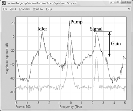
FIGURE 16.14 Optical spectra at the input (light gray-lower) and the output (dark gray-higher) of the OPA.
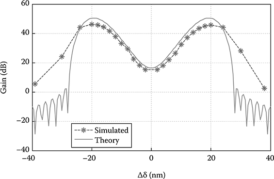
FIGURE 16.15 Calculated and simulated gain of the OPA at Pp = 30 dBm.
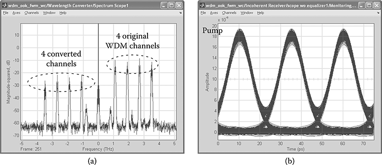
FIGURE 16.16 (a) The wavelength conversion of four WDM channels and (b) eye diagram of the converted 40 Gbps signal after BPF.
Another important application with the same setup is the nonlinear phase conjugation (NPC). A phase-conjugated replica of the signal wave can be generated by the FWM process. From Equation 16.8, the idler wave is approximately given in case of degenerate FWM for simplification: or with the signal wave Es − Asej(kz−ωτ)]. Thus, the idler field is a complex conjugate of the signal field. In appropriate conditions, optical distortions can be compensated for by using NPC, and optical pulses propagating in the fiber link can be recovered. The basic principle of distortion compensation with NPC refers to spectral inversion. When an optical pulse propagates in an optical fiber, its shape will be spread in time and distorted by the group velocity dispersion. The phase-conjugated replica of the pulse is generated in the middle point of the transmission link by the nonlinear effect. On the contrary, the pulse is spectrally inverted where spectral components in the lower frequency range are shifted to the higher frequency range, and vice versa. If the pulse propagates in the second part of the link in the same manner as in the first part, it is inversely distorted again, which can cancel the distortion in the first part to recover the pulse shape at the end of the transmission link. By using NPC for distortion compensation, a 40–50% increase in transmission distance compared to a conventional transmission link can be obtained. Figure 16.17 shows the setup of a long-haul 40 Gbps transmission system demonstrating the distortion compensation using NPC. The fiber transmission link of the system is divided into two sections by an NPC based on parametric amplifier. Each section consists of five spans with 100 km of standard single-mode fiber (SSMF) in each span. Figure 16.18a shows the eye diagram of the signal after propagating through the first fiber section. After the parametric amplifier at the midpoint of the link, the idler signal, a phase-conjugated replica of the original signal, is filtered for transmission in next section. The signal in the second section suffers the same dispersion as in the first section. At the output of the transmission system, the optical signal is regenerated, as shown in Figure 16.18b. Due to the change in wavelength of the signal in NPC, a tunable dispersion compensator can be required to compensate for the residual dispersion after transmission in real systems. A summary of the parameters of the sub-systems of this transmission system is given in Table 16.3.
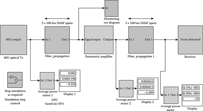
FIGURE 16.17 Simulink® setup of a long-haul 40 Gbps transmission system using NPC for distortion compensation.
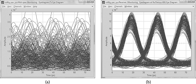
FIGURE 16.18 Eye diagrams of the 40 Gbps signal at the end (a) of the first section and (b) of the transmission link.
16.3.1.2 High-Speed Optical Switching
When the pump is an intensity-modulated signal instead of the CW signal, the gain of the OPA is also modulated due to its exponential dependence on the pump power in a phase-matched condition. The width of gain profile in the time domain is inversely proportional to the product of the gain slope (Sp) or the nonlinear coefficient and the length of the nonlinear waveguide (L). Therefore, an OPA with high gain or large SpL operates as an optical switch with an ultra-high bandwidth, which is very important in some signal processing applications such as pulse compression or short-pulse generation. A Simulink setup for a 40 GHz short-pulse generator is built with the configuration shown in Figure 16.19. In this setup, the input signal is a CW source with low power, and the pump is amplitude modulated by a Mach–Zehnder intensity modulator (MZIM), which is driven by an RF sinusoidal wave at 40 GHz. The waveform of the modulated pump is shown in Figure 16.20a.
TABLE 16.3
Critical Parameters of the Long-Haul Transmission System Using NPC for Distortion Compensation
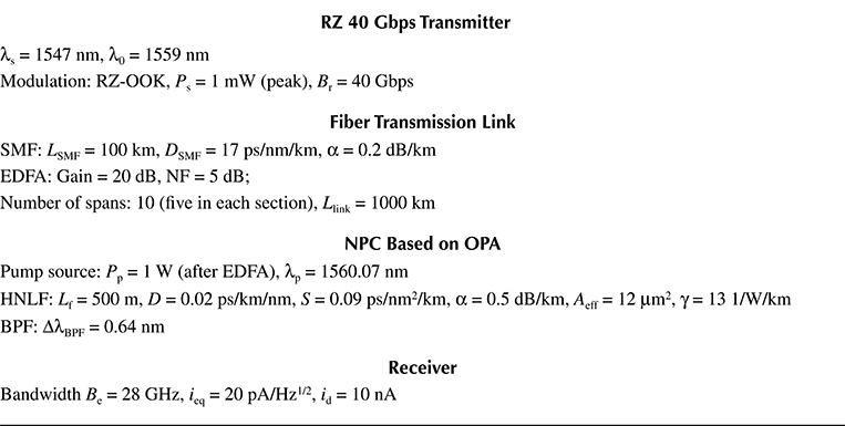
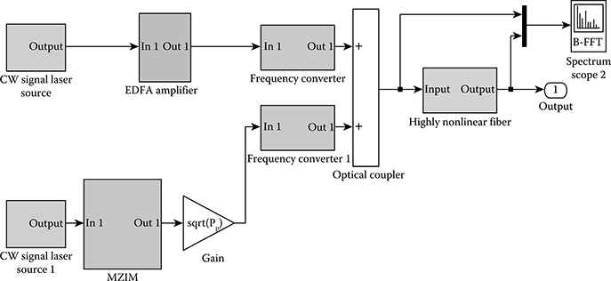
FIGURE 16.19 Simulink® setup of the 40 GHz short-pulse generator.
Important parameters of the FWM-based short-pulse generator are shown in Table 16.4. Figure 16.20b shows the generated short-pulse sequence with a pulse width of 2.6 ps at the signal wavelength after the optical BPF.
Another important application of the optical switch based on the FWM process is the demultiplexer, a key component in ultra-high-speed optical time division multiplexing (OTDM) systems. OTDM is a key technology for Tbps Ethernet transmission that can meet the increasing demand of traffic in future optical networks. A typical scheme of OTDM demultiplexer in which the pump is a mode-locked laser (MLL) to generate short pulses for control is shown in Figure 16.21a. The working principle of the FWM-based demultiplexing is described as follows. The control pulses generated from an MLL at tributary rate are pumped and co-propagated with the OTDM signal through the nonlinear waveguide. The mixing process between the control pulses and the OTDM signal during propagation through the nonlinear waveguide converts the desired tributary channel to a new idler wavelength. Then the demultiplexed signal at the idler wavelength is extracted by a band pass filter before going to a receiver, as shown in Figure 16.21a.
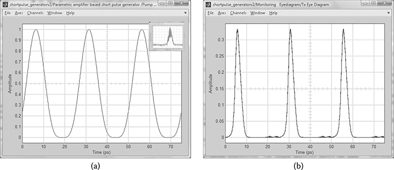
FIGURE 16.20 Time traces of (a) the sinusoidal amplitude modulated pump and (b) the generated short-pulse sequence (inset: the pulse spectrum).
TABLE 16.4
Parameters of the 40 GHz Short Pulse Generator
Short-Pulse Generator |
| Signal: Ps = 0.7 mW, λs = 1535 nm, λ0 = 1559 nm |
| Pump source: Pp = 1 W (peak), λp = 1560.07 nm, fm = 40 GHz |
| HNLF: Lf = 500 m, D = 0.02 ps/km/nm, S = 0.03 ps/nm2/km, α = 0.5 dB/km, Aeff = 12 μm2, γ = 13 1/W/km |
| BPF: ΔλBPF = 3.2 nm |
However, its stability, especially the walk-off problem, is still a serious obstacle. Recently, planar nonlinear waveguides have emerged as promising devices for ultra-high-speed photonic processing. These nonlinear waveguides offer several advantages, such as no free-carrier absorption, stability at room temperature, no requirement of quasi-phase matching, and the possibility of dispersion engineering. With the same operational principle, planar waveguide-based OTDM demultiplexers are very compact and suitable for photonic integrated solutions. Figure 16.21b shows the Simulink setup of the FWM-based demultiplexer of the on–off keying (OOK) 40 Gbps signal from the 160 Gbps OTDM signal using a highly nonlinear waveguide instead of HNLF. Important parameters of the OTDM system in Table 16.5 are used in the simulation. Figure 16.22a shows the spectrum at the output of the nonlinear waveguide. Then, the demultiplexed signal is extracted by the BPF, as shown in Figure 16.22b. Figure 16.23 shows the time traces of the 160 Gbps OTDM signal, the control signal, and the 40 Gbps demultiplexed signal, respectively. The dark gray dots in Figure 16.23a indicate the timeslots of the desired tributary signal in the OTDM signal. The developed model of OTDM demultiplexer can be applied not only to the conventional OOK format, but also to advanced modulation formats such as DQPSK, which increases the data load of the OTDM system without increase in bandwidth of the signal. By using available blocks developed for the DQPSK system shown Figure 16.21b, a Simulink model of the DQPSK-OTDM system is setup for demonstration. The bit rate of the OTDM system is doubled to 320 Gbps with the same pulse repetition rate. Figure 16.24 shows the simulated performance of the demultiplexer in both 160 Gbps OOK-OTDM and 320 Gbps DQPSK-OTDM systems. The BER curve in case of the DQPSK-OTDM signal shows a low error floor, which may be the result of the influence of nonlinear effects on phase-modulated signals in the waveguide.
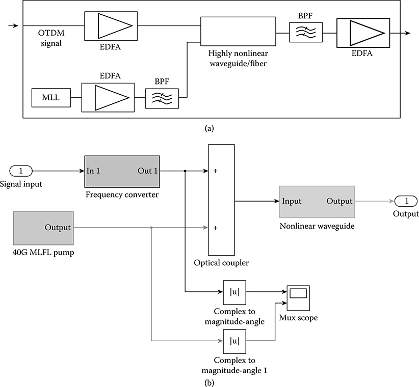
FIGURE 16.21 (a) A typical setup of the FWM-based OTDM demultiplexer and (b) Simulink® model of the OTDM demultiplexer.
TABLE 16.5
Important Parameters of the FWM-Based OTDM Demultiplexer Using a Nonlinear Waveguide
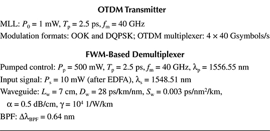
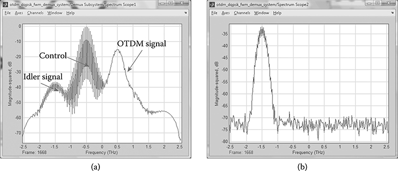
FIGURE 16.22 Spectra at the outputs (a) of nonlinear waveguide and (b) of BPF.
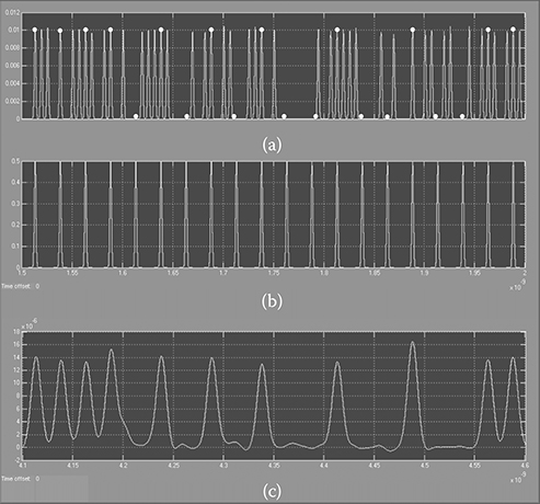
FIGURE 16.23 Time traces of (a) the 160 Gbps OTDM signal, (b) the control signal, and (c) the 40 Gbps demultiplexed signal.
16.3.1.3 Triple Correlation
One of the promising applications exploiting the χ(3) nonlinearity is the implementation of triple correlation in the optical domain. Triple correlation is a higher-order correlation technique, and its Fourier transform, called bispectrum, is very important in signal processing, especially in signal recovery. The triple correlation of a signal s(t) can be defined as
where τ1, τ2 are time-delay variables. Thus, to implement the triple correlation in optical domain, the product of three signals including different delayed versions of the original signal need to be generated and then detected by an optical photodiode to perform the integral operation. From the representation of nonlinear polarization vector (see Equation 16.14), this triple product can be generated by the χ(3) nonlinearity. One way to generate the triple correlation is based on third harmonic generation, where the generated new wave containing the triple-product is at a frequency of three times the original carrier frequency. Thus, if the signal wavelength is in the 1550 nm band, the new wave need to be detected at around 517 nm. The triple optical autocorrelation based on single-stage third harmonic generation has been demonstrated in direct optical pulse shape measurement. However, in this way, it is hard to obtain high efficiency in the wave mixing process due to the difficulty of phase matching between the three signals. Moreover, the triple product wave is in 517 nm, where wideband photo-detectors are not available for high-speed communication applications. Therefore, a possible alternative to generate the triple product is based on other nonlinear interactions such as FWM. From Equation 16.20, the fourth wave is proportional to the product of three waves—. If A1 and A2 are the delayed versions of the signal A3, the mixing of three waves results in the fourth wave A4, which is obviously the triple product of three signals. As mentioned in Section 16.2, all three waves can take the same frequency; however, these waves should propagate into different directions to possibly distinguish the new generated wave in a diverse propagation direction that requires a strict arrangement of the signals in spatial domain. An alternative way we propose is to convert the three signals into different frequencies (ω1, ω2, and ω3). Then the triple-product wave can be extracted at the frequency ω4 = ω1 + ω2 − ω3, which is still in the 1550 nm band.
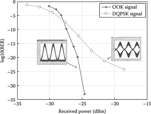
FIGURE 16.24 Simulated performance of the demultiplexed signals for 160 Gbps OOK-OTDM and 320 Gbps DQPSK-OTDM systems (insets: eye diagrams at the receiver).
Figure 16.25a shows the Simulink model for the triple correlation based on FWM in a nonlinear waveguide. The structural block consists of two variable delay lines to generate delayed versions of the original signal, as shown in Figure 16.26, and frequency converters to convert the signal into different three waves before combining at the optical coupler to launch into the nonlinear waveguide. Then, the fourth wave signal generated by FWM is extracted by the passband filter. To verify the triple-product based on FWM, another model, shown in Figure 16.25b, to estimate the triple product by using Equation 16.31, is also implemented for comparison. The integration of the generated triple-product signal is then performed at photodetector in the optical receiver to estimate the triple correlation of the signal.
A repetitive signal, which is a dual-pulse sequence with unequal amplitude, is generated for investigation. Important parameters of the setup are shown in Table 16.6. Figure 16.27 shows the waveform of the dual-pulse signal and the spectrum at the output of the nonlinear waveguide. The wavelength spacing between the three waves is unequal to reduce the noise from other mixing processes. The triple-product waveforms estimated by theory and FWM process are shown in Table 16.6. In case of the estimation based on FWM, the triple-product signal is contaminated by the noise generated from other mixing processes, as indicated in Table 16.6. Figure 16.28 shows the triple correlations of the signal after processing at the receiver in both cases, based on theory and FWM. The triple correlation is represented by a 3D plot, as displayed in the image. The x- and y- axes of the image represent the time-delay variables (τ1 and τ2) in terms of samples with step-size of Tm 32, where Tm is the pulse period. The intensity of the triple correlation is represented by colors with scales specified by the color bar. Although the FWM-based triple correlation result is noisy, the triple correlation pattern is still distinguishable, as compared to the theory. Another signal pattern of single pulse that is simpler has also been investigated, as shown in Figures 16.29 and 16.30.
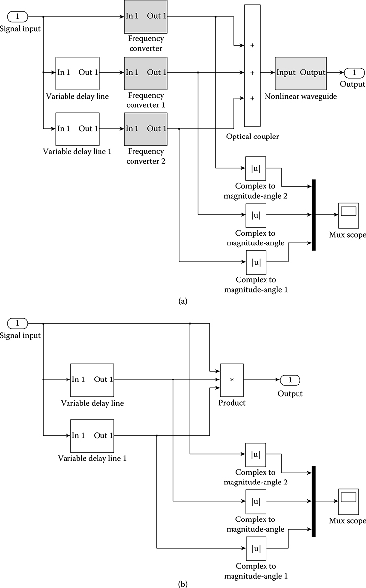
FIGURE 16.25 (a) Simulink® setup of the FWM-based triple-product generation and (b) Simulink setup of the theory-based triple-product generation.
FIGURE 16.26 The variation in time domain of the time delay (gray), the original signal (dark gray), and the delayed signal (light gray).
TABLE 16.6
Important Parameters of the FWM-Based OTDM Demultiplexer Using a Nonlinear Waveguide
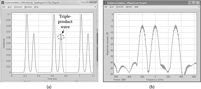
FIGURE 16.27 (a) Time trace of the dual-pulse sequence for investigation and (b) spectrum at the output of the nonlinear waveguide.
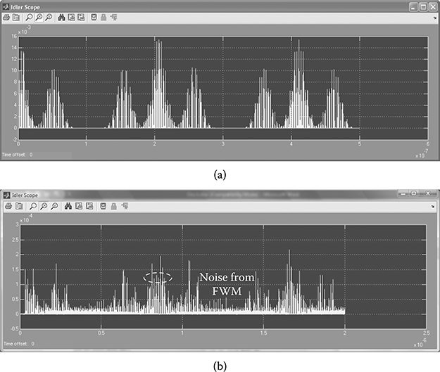
FIGURE 16.28 Generated triple-product waves in time domain of the dual-pulse signal based on (a) theory and (b) FWM in nonlinear waveguide.
16.3.1.4 Remarks
This section demonstrates the employment of an NL optical waveguide and associated NL effects such as parametric amplification, FWM, and third harmonic generation for the implementation of the triple correlation, and thence the bispectrum creation and signal recovery techniques to reconstruct the data sequence transmitted over a long-haul, optically amplified fiber transmission link.
16.3.2 Nonlinear Photonic Preprocessing in Coherent Reception Systems
This section looks at the uses of nonlinear effects and applications in modern optical communication networks in which 100 Gbps optical Ethernet is expected to be deployed.
The typical performance of a photonic signal preprocessor employing no linear FWM is given, and also that of an advanced processing of such received signals in the electronic domain processed by a digital triple correlation system. At least 10 dB improvement is achieved on the receiver sensitivity.
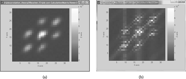
FIGURE 16.29 Triple correlation of the dual-pulse signal based on (a) theoretical estimation and (b) FWM in nonlinear waveguide.
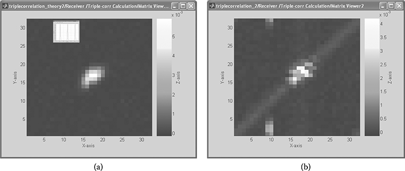
FIGURE 16.30 Triple correlation of the single-pulse signal based on (a) theoretical estimation and (b) FWM in nonlinear waveguide (inset: the single-pulse pattern).
Regarding the nonlinear effects, the nonlinearity of the optical fibers hinders and limits the maximum level of the total average power of all the multiplexed channels for maximizing the transmission distance. These are due to the changes of the refractive index of the guided medium as a function of the intensity of the guided waves. This in turn creates phase changes and hence different group delays, leading to distortion. Furthermore, other associated nonlinear effects such as the four-wave mixing, Raman scattering, Brillouin scattering, intermodulation have also created jittering and distortion of the received pulse sequences after a long transmission distance.
However, we have recently been able to use to our advantage these nonlinear optical effects as a preprocessing element before the optical receiver to improve its sensitivity. A higher-order spectrum technique is employed with the triple correlation implemented in the optical domain via the use of the degenerate FWM effects in a high nonlinear optical waveguide. However, this may add additional optical elements and filtering in the processor and hence complicate the receiver structure. We can overcome this by inserting this nonlinear higher-order spectrum processing sub-system in cascade following the optoelectronic converter and in front of the digital processor (Figure 16.31).
In this section, we illustrate some uses of nonlinear effects and nonlinear processing algorithms for improving the sensitivity of optical receivers employing nonlinear processing at the front end of the photodetector and nonlinear processing algorithm in the electronic domain.
The spectral distribution of the FWM and the simulated spectral conversion can be achieved. There is a degeneracy of the frequencies of the waves, so that efficient conversion can be achieved by satisfying the conservation of momentum. The detected phase states and bispectral properties are depicted in Figure 16.32, in which the phases can be distinguished based on the diagonal spectral lines. Under noisy conditions, these spectral distributions can be observed as depicted in Figure 16.33.
Alternating to the optical processing described earlier, a nonlinear processing technique using HOS technique can be implemented in the electronic domain. This is implemented after the ADC, which samples the incoming electronic signals produced by the coherent optical receiver, as shown in Figure 16.34. The operation of a third-order spectrum analysis is based on the combined interference of three signals (in this case, the complex signals produced at the output of the ADC), two of which are the delayed versions of the original. Thence, the amplitude and phase distribution of the complex signals are obtained in 3D graphs that allow us to determine the signal and noise power, and the phase distribution. These distributions allow us to perform several functions necessary for the evaluation of the performance of optical transmission systems. Simultaneously, the processed signals allow us to monitor the health of the transmission systems—such as the effects due to nonlinear effects, the distortion due to chromatic dispersion of the fiber transmission lines, the noises contributed by in-line amplifiers, and so on. A typical curve that compares the performance of this innovative processing with convention detection techniques is shown in Figure 16.34. If a BER of 1e−9 is required at the receivers employing lower order conventional reception, the high-order spectral receiver described here and associate DSP techniques will improve by at least 1000 times. This is equivalent to at least one unit improvement on the quality factor of the eye opening, which is in turn equivalent to about 10 dB in the SNR.
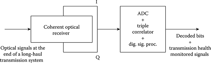
FIGURE 16.31 Schematic diagram of a high-order spectral optical receiver and electronic processing.
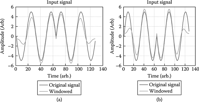
FIGURE 16.32 (a, b) Input waveform with phase changes at the transitions. (c–h) triple correlation and bispectrum of both phase and amplitude under off-line DSP processing.
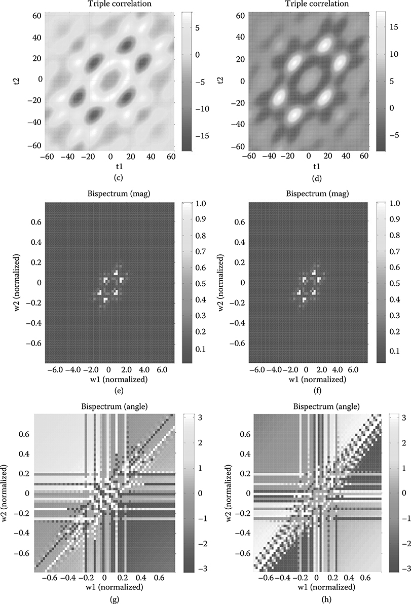
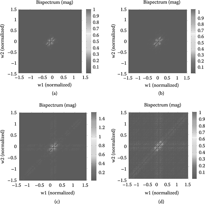
FIGURE 16.33 (a, c) Effect of Gaussian noise on the bispectrum and (b, d) amplitude distribution in 2D phase spectral distribution.
These results are very exciting for network and system operators as significant improvement of the receiver sensitivity can be achieved, and this allows significant flexibility in the operation and management of the transmission systems and networks. Simultaneously, the monitored signals produced by the high-order spectral techniques can be used to determine the distortion and noises of the transmission line, and thus the management of the tuning of the operating parameters of the transmitter, the number of wavelength channels, and the receiver or in-line optical amplifiers.
The effect of additive white Gaussian noise on the bispectrum magnitude is shown in Figure 16.33, and the sequence of figures are as indicated in Figure 16.32. The uncorrupted bispectrum magnitude is shown in Figure 16.32a, while Figure 16.32b through d were generated using SNRs of 10 dB, 3 dB, and 0 dB, respectively. This provides a method of monitoring the integrity of a channel and illustrates another attractive attribute of the bispectrum. It is noted that the bispectrum phase is more sensitive to Gaussian white noise than is the magnitude, and quickly becomes indistinguishable below 6 dB.
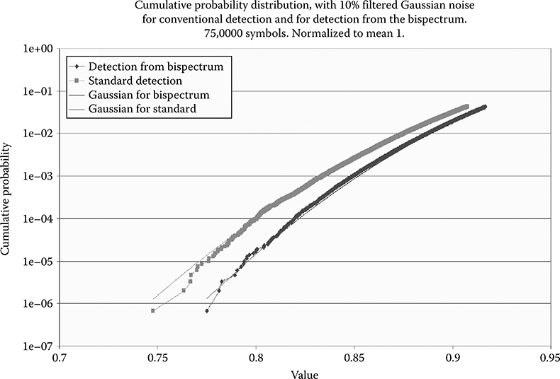
FIGURE 16.34 Error estimation of the detection level of a high-order spectrum processor: cumulative probability of error versus normalized amplitude at OSN of 10 dB.
Although the algorithm employing nonlinear processing will involve both hardware and software implementations, from the practical point of view, it needs to deliver the embedded to the market at the right time for systems and networks operating in Tbps speeds. One can thus be facing the following dilemma.
The optical preprocessing demands an efficient nonlinear optical waveguide, which must be in the integrated structure whereby efficient coupling and interaction can be achieved. If not, then the gain of about 3 dB in SNR would be defeated by this loss. Furthermore, the integration of the linear optical waveguiding section and a nonlinear optical waveguide is not matched due to differences in the waveguide structures of both regions. For a linear waveguide structure to be efficient for coupling with circular optical fibers, silica on silicon would be best suited due to the small refractive index difference and the technology of burying such waveguides to form an embedded structure whose optical spot size would match with that of a single guided mode fiber. This silica on silicon would not match with an efficient nonlinear waveguide made by As2S3 on silicon.
On the contrary, if electronic processing is employed, then it requires an ultra-fast ADC, and then fast electronic signal processors. Currently, a 56 GSamples/s ADC is available from Fujitsu, as shown in Figure 16.35. It is noted that the data output samples of the ADC are structured in parallel forms with the referenced clock rate of 1.75 GHz. Thus, all processing of the digital samples must be in parallel form, and, therefore, parallel processing algorithms must be structured in parallel. This is the most challenging problem that we must overcome in the near future.
An application-specific integrated circuit (ASIC) must also be designed for this processor. Hard decisions must also be made in the fitting of such ASICs and associate optical and optoelectronic components into international standard compatible size. Thus, all design and components must meet this requirement.
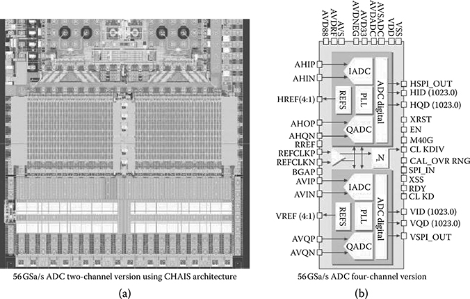
FIGURE 16.35 Plane view of the Fujitsu ADC operating at 56 GSa/s: (a) integrated chip (b) functional schematic of the ADC.
16.4 Concluding Remarks
In this section, we have demonstrated a range of signal processing applications exploiting the parametric process in nonlinear waveguides. A brief mathematical description of the parametric process through third-order nonlinearity has been reviewed. A nonlinear waveguide has been proposed to simulate the interaction of multiple waves in optical waveguides, including optical fibers. Based on the developed Simulink modeling platform, a range of signal processing applications exploiting the parametric FWM process has been investigated through simulation. With a CW pump source, applications such as parametric amplifier, wavelength converter, and optical phase conjugator have been implemented for demonstration. Ultra-high-speed optical switching can be implemented by using an intensity-modulated pump to apply in the short-pulse generator and the OTDM demultiplexer. Moreover, the FWM process has been proposed to estimate the triple correlation, which is very important in signal processing. The simulation results showed the possibility of the FWM-based triple correlation using the nonlinear waveguide with different pulse patterns. Although the triple correlation is contaminated by noise from other FWM processes, it is distinguishable. The wavelength positions as well as the power of three delayed signals need to be optimized to obtain the best results.
Furthermore, we have also addressed the important issues of nonlinearity and its uses in optical transmission systems, and the management of networks if the signals that indicate the health of the transmission system are available. There is no doubt that nonlinear phenomena exert distortion impairments on transmitted signals. However these phenomena can also be exploited to improve the transmission quality of the signals as presented in this chapter. This has been briefly described in this chapter using FWM effects and nonlinear signal processing using high-order spectral analysis and processing in the electronic domain. This ultra-high-speed optical preprocessing and/or electronic triple correlation and bispectrum receivers are the first systems using nonlinear processing for 100–400 Gbps and Tbps optical Internet.
The degree of complexity of ADC and DAC, as well as high-speed DSP, will allow higher-complexity processing algorithms embedded for real-time processing. Thus, higher-order spectral processing techniques will be potentially employed for coherent optical communication with higher dimensional processing.
References
1. J. M. Mendel, Tutorial on high-order statistic (spectra) in signal processing and system theory: Theoretical results and some applications, Proc. IEEE, Vol. 79, No. 3, pp. 278–305, 1991.
2. C. L. Nikias and J. M. Mendel, Signal processing with higher-order spectra, IEEE Sig. Proc. Mag., Vol. 10, No. 3, pp. 10–37, 1993.
3. G. Sundaramoorthy, M. R. Raghuveer, and S. A. Dianat, Bispectral reconstruction of signals in noise: Amplitude reconstruction issues, IEEE Trans. Acoustics, Speech Sig. Proc., Vol. 38, No. 7, pp. 1297–1306, 1990.
4. H. Bartelt, A. W. Lohmann, and B. Wirnitzer, Phase and amplitude recovery from bispectra, Appl. Opt., Vol. 23, pp. 3121–3129, 1984.
5. T. M. Liu, Y. C. Huang, G. W. Chern, K. H. Lin, C. J. Lee, Y. C. Hung, and C. K. Sun, Triple-optical auto-correlation for direct optical pulse-shape measurement, Appl. Phys. Lett., Vol. 81, No. 8, pp. 1402–1404, 2002.
6. D. R. Brillinger. Introduction to polyspectra, Ann. Math. Stat., Vol. 36, pp. 1351–1374, 1965.
7. M. C. Ho, K. Uesaka, M. Marhic, Y. Akasaka, and L. G. Kazovsky, 200-nm-bandwidth fiber optical amplifier combining parametric and Raman gain, IEEE J. Lightwave Technol., Vol. 19, pp. 977–981, 2001.