
14
DSP Algorithms and Coherent Transmission Systems
14.1 Introduction
Digital signal processing (DSP) is the principal functionality of modern optical communication systems employed at both the coherent optical receivers and the transmitter. At the transmitter, DSP is employed for determining the pulse shape at the output of optical modulators, as compensation for the limited bandwidth of the digital-to-analog converter (DAC), as well as that of the transfer characteristics of the electro-optic external modulators, and deskewing of the electrical path differences between the in-phase and quadrature-phase signals that often occur in ultra-high-speed systems. It is noted that the mixing of the received signals and the local oscillator (LO) laser happens in the photodetection stage.
Due to the square law process in the optoelectronic conversion, this mixing gives a number of terms, two square terms related to the intensity of the optical signals and the intensity of the LO laser, and two product terms that result from the beating between the optical signal beam and that of the LO. Only the difference product between these two optical frequencies is detected which is proportional to the signal to be recovered. When the optical frequencies of the signals and the oscillator are the same, the reception process is termed as homodyne coherent detection. If not then the process is a heterodyne type. Thus, provided that perfect homodyne mixing is achieved in the photodetection device, the detected signals, now in electrical domain, are in the baseband, superimposed by noises of the detection process. Thence, after electronic preamplification and then sampled by ADC, the signals are in discrete domain, and thus processed by digital signal processors that can be considered to be similar to processing in wireless communications systems. The main differences are in the physical processes of distortion, dispersion, nonlinear distortion, and clock recovery, broadband properties of optical modulated signals transmitted over long-haul optical fibers or short-reach scenarios.
On the other hand at the receiver end, DSP follows the ADC with the digitalized symbols and processes the noisy and distorted signals with algorithms to compensate for linear distortion impairments such as chromatic dispersion (CD), polarization-mode dispersion (PMD), nonlinear self-phase modulation (SPM) effects, clock recovery, LO frequency offset (FO) with respect to the relieved channel carrier, and so on. A possible flow of sequences in DSP can be illustrated as in Figure 14.1 for modulated channel with the in-phase and quadrature components and polarization multiplexing as recovered in the electronic domain after the optical processing front end as shown at the beginning, the input boxes. Thus, there are two pairs of electrical signal output from the two polarized channels and two for the in-phase and quadrature components. Inter processing of these pairs of signals can be implemented using 2 × 2 multiple-input multiple-output (MIMO) techniques, which are well known in the digital processing of wireless communications signals [1].
After the optoelectronic detection of the mixed optical signals, the electronic currents of the polarization division multiplexing (PDM) channels are then amplified with a linear transimpedance amplifier and a further amplification main stage if required to boost the electric signals to the level at which the ADC can digitalize the signals into their equivalent discrete states. Once the digitalized signals are obtained, the first task would be to ensure that any delay difference between the channels and the in-phase and quadrature components in the electronic and digitalization processes is eliminated by deskewing. Thence, all the equalization processing can be carried out to compensate for any distortion on the signals due to the propagation through the optical transmission line. Furthermore, nonlinear distortion effects on the signals can also be superimposed at this stage. Then, the clock recovery and carrier phase detection can be implemented. Hence, the processes of symbol recovery, decoding, and evaluation of performance can be implemented.

FIGURE 14.1 Flow of functionalities of DSP processing in a QAM coherent optical receiver with possible feedback control. Note that similar chart is also given in Figure 13.1.
Regarding noises in the optical coherent detection the noises are mainly dominated by the shot noises generated by the LO power. However, if direct detection, then the quantum shot noises are contributed by the signal power, and hence are signal dependent. These noises will contribute to the convergence of algorithms.
TABLE 14.1
Functionalities of Subsystem Processing in a DSP-Based Coherent Receiver

This chapter is thus organized as follows. Section 14.2 gives a basic background of equalization using transversal filtering and zero forcing with and without feedback in the linear sense, the linear equalizer. Then when a decision, in a nonlinear sense, is employed under some criteria to feedback to the input sequence, the equalization is nonlinear, and the equalizer is classified as a nonlinear equalizer (NLE) or direct directing (DD) equalizer. Tolerance to noises is also given, and a simple quality factor of the system performance is deduced.
Clock recovery is important for the recovery of the timing for sampling of the received sequence. This technique is briefly discussed in Section 14.4.4. Determining the reference phase for coherent reception is also critical so as to evaluate several quadrature-modulated transmitted signals. Thus, carrier phase recovery technique is also described using DSP techniques, especially in the case when there is significant offset between the LO and the lightwaves carrying the signals. This is described in Section 14.5.
When the maximum-likelihood sequence estimation (MLSE) used in the NLE is employed, the equalization can be considered optimum, but as consuming substantial memory. We dedicate Section 14.3 to this algorithm an example of this MLSE is given to demonstrate its effectiveness of the equalization algorithm in minimum shift keying (MSK) self-homodyne coherent reception transmission systems under the influence of linear distortion effects with the modulation scheme is an MSK. This has already been described in Chapter 12, and is not repeated. The MLSE algorithm is valid for processing individual I and Q components of each polarized channel as in the case of direct detection. We must note here that, under the I–Q modulation, both the I and Q components are modulated as non-return-to-zero modulation formats with a π/2 phase shift in the optical carrier. Thus, when detected, they behave similar to the case of direct detection. Their π/2 phase shift has been taken care of by the hybrid optical coupler. Thus, we can see that four ADC-DSP subsystems are required for coherent PDM-quadrature phase shift keying (QPSK) or PDM-M-ary-quadrature amplitude modulation (QAM) reception systems.
We can thus see that DSP algorithms are most critical in modern DSP-based optical receivers or transponders. This chapter thus introduces the fundamental aspects of these algorithms for optical transmission systems over dispersive channels whether under linear or nonlinear distortion physical effects.
The functionalities of each processing block of Figure 14.1 can be categorized as shown in Table 14.1 [2].
14.2 General Algorithms for Optical Communications Systems
Indeed, in coherent optical communication systems incorporating DSP, the reception of the transmitted signals by mixing them with a LO whose frequency is identical or close to equality which is known as the homodyne or intradyne reception techniques. The coherent reception converts the optical signals back to the baseband whose phase and amplitude is complex and distorted due to the transmission medium. The received signals are now transformed back to the digital domain and can thus be processed by a number of digital processing algorithms as previously developed for high-speed modems [3] or in wireless communication systems [4].
Naturally, a number of steps of conversions from optical to electrical and vice versa at the receiver and transmitter have to be conducted with further optical amplifier noises accumulated along the optical transmission line and electronic noises.
In this chapter, we assume that the signal level is quite high as compared to the electronic noise level at the output of the electronic preamplifier that follows the photodetector. Hence, the processing algorithms are conducted in the baseband electrical digital domain after the ADC stage.
14.2.1 Equalization of DAC-Limited Bandwidth for Tbps Transmission
This section considers algorithms developed to compensate for the band-limited DAC, especially the generation of 28 and 32 GBaud PDM-Nyquist-QPSK by a DAC with an analog bandwidth of only 11.3 GHz [5].
14.2.1.1 Motivation
For realizing ultra-high-capacity optical fiber networks, it is extremely important to improve the spectral efficiency in wavelength-division-multiplexed (WDM) transmission systems. High-order modulation formats such as M-ary phase shift keying (PSK) and QAM offer efficient solutions [6,7]. However, further improvement can be achieved by using the well-known “Nyquist pulse shaping” technique [8], applicable to any modulation format. This technique relies on tight signal filtering squeezing the signal bandwidth very close to the symbol rate, meanwhile maintaining zero inter-symbol interference (ISI). In order to minimize the penalty due to crosstalk between closely spaced WDM channels, it is required to reshape the optical spectrum either in optical domain by narrow optical filtering, or, in the electrical domain, by shaping the driving signals applied to optical modulators by combining DSP and DAC.
The main drawback of performing spectrum shaping in the optical domain is the requirement for a very specific transfer function of the optical filter, which may be cost-ineffective and bulky. Alternatively, it is more simple and efficient to generate the Nyquist pulse for any modulation format using transmitter DSP and DAC. Several Nyquist experiments using lower-rate DACs have been reported recently, for example, generation of 9 GBaud PDM-Nyquist-32QAM with a roll-off factor (ROF) of 0.01 using 24 GSa/s DAC [9], Nyquist pulses at 14 GBaud of PDM-16QAM generated by 28 GSa/s DAC [10]. For the generation of Nyquist pulse with high baud rate, one critical limitation comes from the electrical bandwidth at transmitter side, which is dominated by DAC, RF driver, and I–Q modulator. And, in almost all the publications, pre-equalization for this limitation is mentioned.
In this section, we evaluate improvements from bandwidth limitation pre-equalization by considering the generations of 28 and 32 GBaud PDM-Nyquist-QPSK using a DAC working at 2 Sa/s with 11.3 GHz analog bandwidth and 8-bit resolution. As described in Chapter 3, the Nyquist waveform can be generated by the use of off-line DSP and loading to the associate memory for execution in the DAC. A root-raised-cosine (RRC) filter is implemented in frequency domain and combined with a pre-equalizer to compensate for the limited Tx electrical bandwidth. Optical/electrical signal spectrums and eye diagrams together with respectable improvements characterize the limits of high-speed Nyquist signal generation, and the fastest DAC devices reported here will speed up the practical deployment of DAC in ultra-high-bit-rate superchannel transmissions.
14.2.1.2 Experimental Setup and Bandwidth-Limited Equalization
The experimental setup used in our investigation is shown in Figure 14.2. The output of an external cavity laser (ECL) with a linewidth of 100 KHz is coupled to a PDM I–Q modulator driven by a DAC with four independent outputs. Driving signals are generated by off-line DSP and loaded to the DAC evaluation board. To generate the Nyquist waveform, pseudo-random-bit sequences of length 215−1 are used in bit-to-symbol mapping to generate the in-phase and quadrature signals, which are then up-sampled to 2 Sa/s and followed by an RRC filter of an ROF of 0.01.
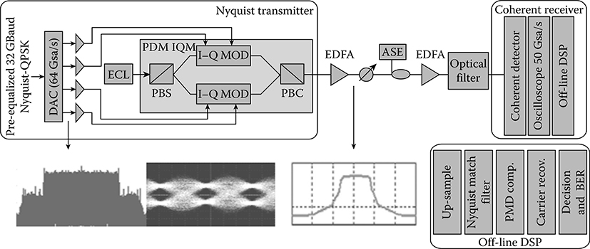
FIGURE 14.2 Experimental setup of 128 Gbps Nyquist PDM-QPSK transmitter and BTB.
The Nyquist filter has 256 taps and is implemented in the frequency domain. This implementation brings the advantage that bandwidth limitation pre-equalization can be combined with Nyquist pulse shaping, but only one set of FFT/IFFT for each data path is required, and this allows significant reduction of DSP complexity avoiding two separate filters dedicated for Nyquist pulse shaping and bandwidth limitation pre-equalizer, respectively. The DAC is operated at the sample rate of 56 and 64 GSa/s, leading to the symbol rate of 28 and 32 GBaud, respectively (twofold oversampling). The outputs of DACs are amplified by four RF drivers before feeding into the PDM I–Q modulator. Unlike other reports of Nyquist pulse generation at lower speeds, no antialiasing low-pass electrical filter is used to filter out spurious frequency components before drivers. They have already been attenuated after DACs, thanks to the DAC-limited bandwidth being quite below half of the baud rate. Voltages controlling RF driver amplification are carefully adjusted, so that the output amplitudes modulating MZMs are twice less than the Vπ value eliminating nonlinear effect introduced by the MZM nonlinear transfer function. The generated optical Nyquist signal is then combined with ASE noise generated by an erbium-doped fiber amplifier (EDFA) before being amplified and filtered by a 50 GHz optical filter to prevent shooting noise effects.
After optoelectrical conversion using a polarization- and phase-diverse coherent receiver, four electrical signals are captured by a four-channel 50 GSa/s oscilloscope with an analog bandwidth of 20 GHz (million samples per line). The captured data are then processed off-line including up-sampling, Nyquist matched filtering (RRC filter), recovering polarization by an 11-tap 2 × 2 MIMO adaptive equalizer, carrier frequency and phase recovery (Viterbi & Viterbi), hard limiter, and bit-error-rate (BER) measurement.
To derive the transfer function later used for pre-equalization, two approaches are evaluated: (1) based on DAC’s bandwidth characteristics only, and (2) based on the whole electrical and optical filtering effects at the transmitter side. For the former one, we determine the DAC transfer function by driving it with sinusoid waveforms at different frequencies, and the result is shown in Figure 14.3j, in which a 3 dB bandwidth of around 11.3 GHz can be observed. Applying approach (2), the transfer function of the whole transmitter side is obtained by comparing the optical spectrum after PDM I–Q modulator with the ideal Nyquist spectrum. BTB performance comparison between these two approaches is shown in Figure 14.4a. The Q factor difference is calculated by subtracting the Q factor of approach (2) from that of approach (1). And both methods result in similar performance, with a bit more emphasized performance for approach (1). Intuitively from this figure, one can conclude that the bandwidth limitation mainly comes from the DAC side. Therefore, all the following pre-compensation results are based on only the DAC’s transfer function.

FIGURE 14.3 (a, b) Spectrum and (e, f) eye diagram of RF signals after DAC without pre-equalization at 28/32 GBaud setup; (c, d) spectrum and (g, h) eye diagram of RF signals after DAC with pre-equalization at 28/32 GBaud setup; (i) noise character of DAC; (j) measured DAC bandwidth character; (k, l) optical spectrums of signals after PDM IQM at 28/32 GBaud setup, light/dark gray line for without/with pre-equalization.

FIGURE 14.4 (a) Q factor difference between different transfer functions (all transmitter side imperfection based and only DAC’s limited bandwidth based) used for pre-equalization in 32 GBaud system; (b) Q factor improvement from pre-equalization in 28 and 32 GBaud systems. OSNR = optical signal-to-noise ratio.
Impacts caused by the limited bandwidth of the transmitter side for a 28 GBaud system can be observed from Figure 14.3a and the light gray line in Figure 14.3k, which depict the electrical and optical spectrums at the outputs of the DAC and the PDM I–Q modulator, respectively. The Gaussian-like slopes caused by the limited bandwidth can be observed. Furthermore, from the eye diagram shown in Figure 14.2e, the clear transient patterns caused by the non-Nyquist filtering are visible. Similar but stronger influence from the limited bandwidth in case of a 32 GBaud system can be observed from Figure 14.3b and the light gray line in Figure 14.3l.
The effectiveness of pre-equalization for a 28 GBaud system can be observed from both the electrical and optical spectrums depicted in Figure 14.3c and the dark gray line in Figure 14.3k, respectively. In the passband, the spectrums are almost as flat as those of an ideal Nyquist signal, except the side lobes (stopband) caused by DAC noise (will be discussed later).
By examining the eye diagrams of the pre-equalized 28 GBaud RF signal depicted in Figure 14.3g, we can observe that there are no longer any transient patterns, and that the eye opening at the optimum sampling point is only half of that of the nonequalized one. Similar observations come from the electrical/optical spectrum and eye diagram of the 32 GBaud system presented in Figures 14.3d and 14.3l. Improvements from pre-equalization in terms of Q factor (versus optical-signal-to-noise ratio [OSNR]) are presented in Figure 14.4b. More than 0.8 dB is achieved in both scenarios, 28 and 32 GBaud systems. It should be noticed that the side lobes in all the electrical spectrums with or without pre-equalization in Figure 14.3 come from the intrinsic noises of the DAC device. Depicted in Figure 14.3i is the spectrum of output signal from DAC under zero input driving signals. Although the noise is supposed to follow Gaussian distribution with a flat spectrum except for some clock crosstalk, an oscilloscope with 20 GHz bandwidth used to capture the noise gives the steep cutoff edge at around 20 GHz, and a similar spectral shape can be observed as the side lobes of the spectrums shown in Figure 14.3a and d.
Therefore, in this section, the generations of 28 and 32 GBaud PDM-Nyquist-QPSK by a DAC with the sample rates up to 64 GSa/s and 11.3 GHz analog bandwidth is presented to address the band-limited problem of DAC whose sampling rate is a very high 64 Gbps. The impacts from the limited bandwidth of the DAC are evaluated in terms of electrical/optical spectrums and eye diagrams, and the corresponding pre-equalization can bring more than 0.8 dB Q factor gain.
14.2.2 Linear Equalization
Coherent optical communication systems can be considered synchronous serial systems. In transmitting optical signals over uncompensated optical fiber that spans over long-haul multispan links or uncompensated metropolitan networks at very high bit rates (commonly, now in the second decade of the twenty-first century, at 25 or 28–32 GSy/s, including forward error coding overloading), the received signals are distorted due to linear and nonlinear dispersive effects, hence leading to ISI in the baseband after coherent homodyne detection at the receiver. In Chapters 4 and 5 we have described in detail the processes of coherent detection, especially homodyne reception for optical signals including noise processes. Over the nondispersion-compensating multispan fiber links, the most important signal distortion is the linear CD and PMD, especially when PDM is employed and two polarization orthogonal channels are simultaneously transmitted. The ISI naturally occurs due to the band-limiting of the signals over the limited bandwidth of the long fiber link, as described in Chapter 2 on the transfer function of optical fibers. Other nonlinear distortion effects have also been included in the transfer function as indicated by the nonflatness of the passband of the transfer function of the fiber. These ISI effects will degrade the performance of the optical communications and need to be tackled with the equalization processes that are discussed in this chapter.
The optical coherent detection processes and DSP of sampled digital signals may be classified into two separate groups.
The first of these, the received sampled digital signals, are fed through an equalizer that corrects the distortion introduced by the CD and PMD effects and restores the received signals into a copy of the transmitted signals in the electrical domain. The received signals are then detected in the conventional manner as applied to any serial digital signals in the absence of ISI. In other words, the equalizer acts as the inverse of the channel, so that the equalizer and the channel together introduce no signal distortion, and each data symbol is detected as it arrives, independently of each other. The equalizers can be either linear or nonlinear.
In the second group of detection processes, the decision process is modified to take into account the signal distortion that has been introduced by the channel, and no attempt need, in fact, be made here to reduce signal distortion prior to the actual decision process. Although no equalizer is now required, the decision process may be considerably complex, and hence complex algorithms are needed to deal with this type of decision processing.
In addition to these two decision groups, there are additional issues to resolve, involving the synchronization of the sampling at the receivers, the clock recovery, and carrier phase estimation, so that a reference clocking instant can be established, and the referenced phase of the carrier can be used to detect the phase states of the received samples. Concurrently, any skew or delay differences between the I and Q components as well as the polarized multiplexed channels must be detected and deskewed, so that synchronous processes can be preserved in the coherent detection processes. Although they remain in practical implementation under software control, these physical processes are not included in this book’s chapters.
Furthermore, any delay difference due to different propagation time of the two different polarized channels or due to different lengths of the electrical connection lines, then a deskewing process can be conducted to minimize these effects, as shown in Figure 14.1.
Thus, in the following section, the LE process is introduced.
14.2.2.1 Basic Assumptions
In general, a simplified block diagram of the coherent optical communication system can be represented in the baseband, that is, after optical field mixing, and detected by optoelectronic receivers and E/O conversion at the transmitter, as shown in Figure 14.5. The input to the transmitter is a sequence of regularly spaced impulses, assuming that the pulse width is much shorter than that of the symbol period, which can be represented by , with Si of binary states taking both positive and negative values as the amplitude of the input signal sequence; thus, we can write

FIGURE 14.5 Simplified schematic of coherent optical communication system. Note equivalent baseband transmission systems due to baseband recovery of amplitude and phase of optically modulated signals.
Thus, the impulse sequence is of a binary polar type. This type of signal representation is advantageous in practice as it can be employed to modulate the optical modulators, especially the Mach–Zehnder interferometric modulator (MZIM), or the I–Q modulator as described in Chapter 3, so that the phase of the carrier under the modulated envelope can take positive or negative phase angles, which can be represented on the phasor diagram. In practice, the impulse can naturally be replaced by a rectangular or rounded or Gaussian waveform by modifying the transmitter filter, which can be a Nyquist raised-cosine type to tailor the transmitting pulse shape.
It is further noted that the phase of the optical waves and the amplitude modulated by the I- and Q-MZIM in the two paths of the I–Q modulator ensure the negative and positive position of the I and Q components on the real and imaginary axes of the constellation, as shown in Figure 3.42. Under coherent reception, these negative and positive amplitudes and phases of the signals are recovered in the electrical domain with superimposed noises. We can see that the synchronization of the modulation signals fed into the two MZIMs is very critical in order to avoid degradation of the sampling instant due to skewing.
14.2.2.2 Zero-Forcing Linear Equalization
Consider a transmission system and receiver subsystem as shown in Figure 14.6, in which the transmitter transfer function can be represented by HTx(f), the transfer function of the channel in linear domain by HC(f), and the transfer function of the equalizer or filter by HEq(f), which must meet the condition for the overall transfer function of all subsystems equating to unity
Thus, from Equation 14.2, we can obtain, if the desired overall transfer response follows that of a Nyquist raised-cosine filter, the equalizer frequency response as
With the raised-cosine function defined with β as the ROF as the frequency response of the equalizer
Implying that the filter is a Nyquist filter of raised-cosine shape; ω is signal baseband frequency; and t0 is the time at the observable instant. In case two channels are observed simultaneously, the right-hand side of Equation 14.2 is a unity matrix and the unitary condition must be satisfied—that is, the conservation of energy.
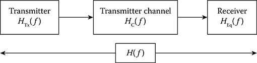
FIGURE 14.6 Schematic of a transmission system including a zero-forcing equalizer/filter.
From Equation 14.3, the magnitude and phase response of the equalizer can be derived. This condition guarantees a suppression of the ISI, and thus the equalizer can be named as a linear equalizer (LE) zero-forcing (ZF) filter (LE-ZF).
14.2.2.3 ZF-LE for Fiber as Transmission Channel
The ideal zero-forcing equalizer is simply the inverse of the channel transfer function given in Equation 14.2. Thus, the required equalizer transfer function HEq(f) is given by
where ω is the radial frequency of the signal envelope, and α is the parameter dependent on the dispersion, wavelength, and velocity of light in vacuum as described in Chapter 4. However, this transfer function does not maintain conjugate symmetry, that is
This is due to the square law dependence of the dispersion parameter of the fiber on frequency.
Thus, the impulse response of the equalizing filter is complex. Consequently, this filter cannot be realized by a baseband equalizer using only one baseband received signal, which explains the limited capability of LEs employed in direct detection receivers to mitigate the CD. On the other hand, it also explains why fractionally spaced LEs that are used within a coherent receiver can potentially extend the system to reach distances that are only limited by the number of equalizer taps [11]. Under coherent detection, and particularly the QAM, both real and imaginary parts are extracted separately and processed digitally. The schematic of a fractionally spaced finite impulse response (FIR) filter is shown in Figure 14.7, in which the delay time between taps is only a fraction of the bit period. The weighting coefficients W0(n),...,WN−1(n) are determined, and then multiplied with the signal paths S(n) at the outputs of the taps. These outputs are then summed up and subtracted by the expected filter coefficients d(n) to obtain the errors of the estimation. This process is then iteratively operated until the final output sequence Y(n) is closed to the desired response.
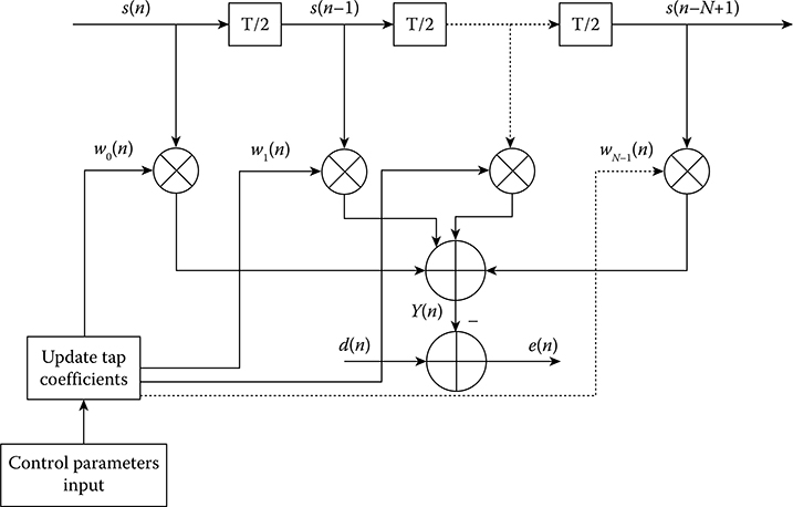
FIGURE 14.7 Schematic of a fractionally spaced finite impulse response (FIR) filter.
Under ZFE, at the sampling instant, the noise may have been increased due to errors in the delay of the zero crossing point of adjacent pulses, hence inter symbol interference (ISI) effects. Thus, the signal-to-noise ratio (SNR) may not be optimum.
The number of taps must cover the whole length of the dispersive pulses—for example, for a 1000 km standard single-mode optical fiber (SSMF) transmission line, where the BW of the channel is 25 GHz (or ~0.2 nm at 1550 nm), the total pulse spreading is 17 ps/nm/km × 1000 km × 0.2 nm = 3400 ps. Sampling rate would be 50 GSa/s (two samples per period @ 25 Gbps, assuming that modulation results in the BW equal to symbol rate), and one would then have 3400/40 periods or ~85 periods or taps with 170 samples altogether.
14.2.2.4 Feedback Transversal Filter
Transversal equalizers have been considered so far as linear feed-forward (FFE) transversal filters commonly employed in practice over several decades since the invention of digital communications. Equalization may alternatively be achieved by feedback transversal filters, provided certain conditions can be met by the channel responses—in this case, the linear transfer function of the fiber transmission line.
Let the z-transform of the sampled impulse response of the channel, which is the optical fiber under the modulated lightwave propagation connected in series with the receiving sub-systems, as
where y0 ≠ 0, and let V(z) be the z-transform derived from the scaling of Y(z), so that the first term becomes unity. Thus, we have
or, written in cascade factorized form,
where βi can be real or complex valued. The feedback transversal filter can then be configured as shown in Figure 14.8, which follows the operation just described. Obviously, the received sequence is multiplied with a factor 1/y0 in order to normalize the sequence, and delayed by one period with a multiplication ratio then summed up and feedback to subtract with the normalized incoming received sequence. The output is taped from the feedback path as shown in the diagram, at the point where the transversal operation is started.
14.2.2.5 Tolerance to Additive Gaussian Noises
Consider a linear FFE with (m + 1) tap as shown in Figure 14.9, assuming that the equalizer has equalized the input signals in the baseband so that the output of the equalizer is given as
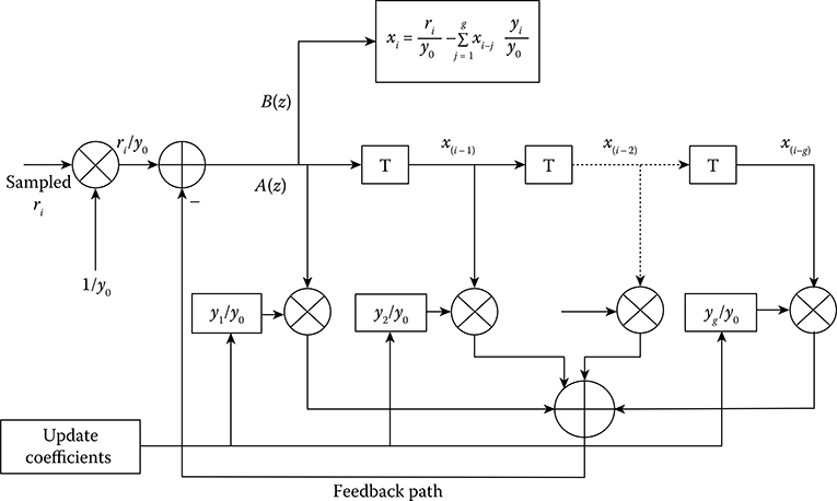
FIGURE 14.8 Schematic structure of a linear feedback transversal equalizer for a channel of a z-transform impulse response Y(z).
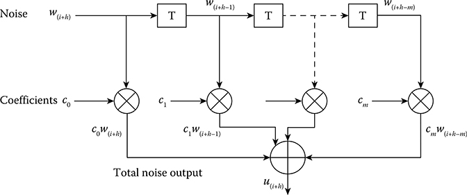
FIGURE 14.9 Noisy signals in an (m + 1) tap linear FFE.
Note that noise always adds to the signal level, so that, for positive k, the noise ui+h follows the same sign (and vice versa for negative value).
The output noise signals of the FFE can thus be written as
The noise components {wi} are statistically independent Gaussian random variables with zero mean and a variance of σ2, so that the total accumulated noise output given by Equation 14.11 is also an uncorrelated random Gaussian variable with zero mean and a variance of
where |C| is the Euclidean length of the (m + 1) component vector [C] = [c0 c1 ...... cm], the sampled channel impulse response. Thus, η2 is the mean square noise of the process and is also the mean square error (MSE) of the output sampled values xi+h.
Thus, the probability noise density function of this Gaussian noise is given by
Thus, with the average value of the magnitude of the received signal in sampled value of k which are equalized with no residual distortion, then the probability of error of the noisy detection process is given by
And, the electrical SNR is given as
with Q(x) as the quality function of x, that is, the complementary error function as commonly defined. In practice, this SNR can be measured by measuring the standard deviation of the constellation point and the geometrical distance from the center of the constellation to the central point of the constellation point. One can see in the next section that the equalized constellation would offer much higher SNR as compared with that of the non equalized constellation. Thus, under Gaussian random distribution, the noises that contribute to the equalization process are also Gaussian, and the probability density function and the Euclidean distance of the channel impulse response can be found without much difficulties.
14.2.2.6 Equalization with Minimizing MSE in Equalized Signals
It has been recognized that a linear transversal filter that equalizes and minimizes the MSE in its output signals [12, 13 and 14] generally gives a more effective degree of equalization than an equalizer that minimizes the peak distortion. Thus, an equalizer that minimizes the mean square difference between the actual and ideal sampled sequence at its output for a given number of taps would be advantageous when noises are present.
Now, revisiting the transmission given in Figure 14.9 in which the sampled impulse response of the channel, the sampled impulse response of (m + 1) tap linear FFE, and the combined sampled impulse response of channel and the equalizer, [Y], [C], and [E], respectively, are given by
Under the condition that the impulse response of the channel is combined with that of the equalizer so that the recovered output sequence is only a pure delay of h sampling periods, the input sampled sequence we have
Or it is a pure delay superimposed by the Gaussian noises of the transmission line. For the case of optically amplified multispan transmission link, the system noises are the accumulated ASE noises of the optical amplifiers placed in each span. Thus, the resultant ideal vector at the output of the equalizer can be written as
However, in fact, the equalized output sequence would be (as seen from Equation 14.16)
The input sampled values are statistically independent and have equal probability of taking values of ±k, and this indicates that the expected value (denoted by the symbol ξ[.]) is
The noises superimposed on the sampled values are also statistically independent of the sampled signals with zero mean, and thus the sampled signals and noises are orthogonal, so we have the expected value ξ[Si+h−jui+h] = 0.
Thus, an LE that minimizes the MSE in its output signals would also minimize the mean square value of [xh+i − si], which can be written as
with
where |E − Eh| and |C| are the Euclidean distances of the vector [E − Eh] and C = [C], respectively. We can now observe that the first and second terms of Equation 14.21 are the MSEs in xi + h due to ISI and the MSE due to Gaussian noises. Thus, we can see that the MSE process minimizes not only the distortion in terms of the MSE due to ISI but also that of the superimposing noises.
14.2.2.7 Constant Modulus Algorithm for Blind Equalization and Carrier Phase Recovery
14.2.2.7.1 Constant Modulus Algorithm
Suppose that intersymbol interference, additive noise, and carrier FO are considered. Then, a received signal before processing, x(k), can be written as
where h(k) is the overall complex baseband-equivalent impulse response of the overall transfer function, including the transmitter, unknown channel, and receiver filter. Note that all E/O and O/E with coherent reception steps are removed. Furthermore it is assumed that there are only noises contribution but no distortion in both phase and amplitude components of the received complex quantities. n(k) are the overall noises which are assumed to be Gaussian, mainly due to ASE noises over cascaded amplifiers with zero mean and standard deviation amount. The input data sequence a(k−i) is assumed to be independent and identically distributed, and φ(k) is the carrier phase difference between the signal carrier and LO laser.
Now let the impulse response of the equalizer be W(k); as denoted in the schematic given in Figure 14.10, the output of the equalized signals can be obtained by
where W(k) = [w0, w1,…… wk]T, the tap weight vector of the equalizer, as described in the preceding sections of this chapter, and X(k) = [x(k), x(k − 11),…… x (k − N + 1)]T is the vector input to the equalizer, where N is the length of the weight vector.
In fiber transmission, there is a pure phase distortion due to the CD effects in the linear region, and the constellation is rotating in the phase plane. In addition, the carrier phase also creates additional spinning rotation of the constellation, as observed in Equation 14.22. Thus, in order to equalize the linear phase rotation effects, one must cancel the spinning effects due to this carrier phase difference created by the mixing between the LO and the signal carrier. Thus, we can see that the constant modulus algorithm must be associated with the carrier phase recovery, so that an additional phase rotation in reverse would be superimposed on the phase rotation due to channel phase distortion to fully equalize the constellation.

FIGURE 14.10 Equivalent model for baseband equalization: (a) blind constant modulus algorithm (CMA), and (b) modified CMA by cascading CMA with carrier phase recovery. Signal inputs come from the digitalized received samples after coherent reception. DPC = differential phase compensation.
The constant modulus (CM) criterion may be expressed by the nonnegative cost function Jcma, p, q, parameterized by positive integers p and q, such that
where E(.) indicates the expected statistical value. The CM criterion is usually implemented as constant modulus algorithm (CMA) 2−2, where p, q = 2. Using this cost function, the weight vectors can be updated by writing
where Rp is the constant depending on the type of constellation. Since the final output of the equalizer system would converge to the original input states, one can rewrite Equation 14.25 as
Assuming that the in-phase and quadrature-phase components of a(k) to be de correlated with each other and using of the input sequence a(k) and the convolution with the impulse response of the channel h(k) we have x(k) = h(k) · a(k), the constant Rp can be determined as
The flow of the update procedure for the weight coefficients of the filter of the equalizer is shown in Figure 14.11.
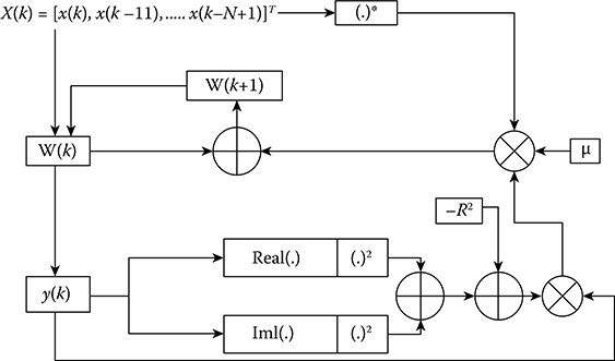
FIGURE 14.11 Block diagram of tap update with CMA cost function.
14.2.2.7.2 Modified CMA: Carrier Phase Recovery Plus CMA
As we know from the cost function (Equation 14.24) used in the CMA, since the cost function is phase-blind, the CMA can converge even in the presence of the phase error. Although it is the merit of the CMA, at convergence, the equalizer output will have a constant phase rotation. This phase rotation is commonly due to the difference of the frequency of the LO and the carrier or LOFO (LO frequency offset). Furthermore, the constellation will be spinning at the carrier FO rate (considered as the phasor rotation) owing to the lack of carrier frequency locking. While this phase-blind nature of the CMA is not a serious problem for constant phase rotation, for some parameters, such as the random PMD and the fluctuation of the phase of the carrier, for example, the 100 MHz oscillation of the feedback mirror in the external cavity of the LO, the performance of the CMA is severely degraded by the randomly rotating phase distortion. Thus, the carrier phase recovery is essential to determine the LOFO, the offset of the LO, and the carrier of the signal channel. The block diagram of the combined CMA blind equalization and carrier tracking and locking is illustrated in Figure 14.10. The carrier recovery (CR) loop uses the error between the output of the equalizer and the corresponding decision. The phase updating rule is given by ϕk + 1) = ϕk ) μϕ I[z(k)e * (k)], where μϕ is the step-size parameter, e(k) is the error signal, given by e(k) = z(k) − â(k), z(k) = y(k) e−jf(k) is the equalized output with phase error correction, and â(k) is the estimation of z(k) by a decision device. The carrier tracking loop described earlier gives the estimate of the phase error, as shown in Figure 14.10b. Then, a differential phase compensation (DPC) can be implemented.
The modified CMA is implemented by cascading the carrier phase recovery first and then cascaded with the standard CMA, as shown in Figure 14.11. A typical CMA operation with carrier phase recovery is shown in Figure 14.12, for the 16QAM constellation with the optical coherent transmission and reception described in Chapter 4, in which a 100 MHz oscillation of the LO laser is observed. We can observe that the constellation of the nonequalized processing is noisy and certainly cannot be used to determine the BER of the transmission system. However, as observable in Figure 14.12b, if only the CMA algorithm is employed, then the phase rotation due to the phase offset between the LO and the signal channel carrier can still exist. When carrier phase recovery is applied, the constellation can then be recovered as shown in Figure 14.12c and d, with and without the DD processing stages, which offer similar constellations. The DD processing will be described in the Section 14.2.3.1 dealing with NLEs or decision feedback equalizers (DFEs) in this chapter.

FIGURE 14.12 Constellations of 16QAM modulated signals with a carrier frequency offset with respect to that of the LO laser. (a) Unequalized output, (b) output equalized by CMA, (c) output by joint CMA and carrier phase DD recovery, and (d) output by modified CMA, carrier phase recovery and CMA processes in sequential stages.
Noe et al. [15] has reported simulation of coherent receivers under polarization multiplexed QPSK employing CMA algorithms under standard and modification in association with the original and modified DD algorithms. Furthermore there are some certain penalties to within 0.5 dB, on the receiver sensitivity.
14.2.3 NLE or DFE
14.2.3.1 DD Cancellation of ISI
It has been demonstrated in both wireless and optical communications systems over recent years that nonlinear (decision feedback) equalizers achieve better performance than their linear counterparts. The method of operation of these DD equalizers for cancellation of ISI is as follows.
Consider the transmission systems given in Figure 14.13a, which is also similar to Figure 14.5, except that the LE is replaced with a nonlinear one. The linear FF equalizer or transversal filter in this NLE is given in Figure 14.13c. The arrow directing from the decision block across the FF transversal filter indicates the updating of coefficients of the filter.
Similar to the LE case, the input sampled data sequence also follows the notations given in Section 14.2. Multilevel data-symbol can be treated in the same way without unduly affecting any of the important results in this analysis.
The pure NLE uses the detected data symbols to synthesize the ISI component in a received signal {ri}, and then it removes the ISI by subtraction. This is the process of DD cancellation of ISI.
Mathematically setting by following the notation used from Equation 14.10 for the section just before the decision/detection block of Figure 14.13a, or the sampled sequence at the input of Figure 14.13b, the signals entering the detector at the instant t = iT is given as
So that, with corrected detection of each sampled value si−j such that
So that, in the correct detection and equalization, we have recovered the sampled sequence {xi}. Thus, it is clear that, as long as the data symbols {si} are correctly detected, their ISI is removed from the equalized signals followed by the NLE, and the channel continues to be accurately equalized.
Under the tolerance of this pure NLE operating in a channel-sampled impulse response whose z-transform given by {Y(z)} in Equation 14.5, the equalized sampled signals at the detector input can be expressed by
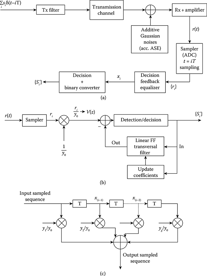
FIGURE 14.13 (a) Simplified schematic of coherent optical communication system incorporating an NLE. Note equivalent baseband transmission systems due to baseband recovery of amplitude and phase of optically modulated signals. (b) Structure of the DFE employing linear FFE and a decision device. (c) Structure of the FF transversal filter.
It is assumed that the sampled sequence is detected as +k or –k, depending on whether xi takes negative or positive values. Errors would occur if the noise levels corrupt the magnitude, that is, if the noise magnitude is greater than k. As in the previous Section 14.2.2.5, with respect to the Gaussian noise contributing to the decision process, we can obtain the probability density function of the random variable noise, w, as
The probability of error can be found as
The most important difference between NLEs and LEs is that the NLE can handle the equalization process when there is pulse on the unit circle of the z-plane of the z-transform impulse response of the transmission channel.
A relative comparison of the LE and NLE is as follows:
When all zeroes of the channel transfer function in the z-plane lie inside the unit circle in the z-plane, the NLE with samples including the initial instant would gain an advantage to the tolerance of the Gaussian additive noise over that of LE. The NLE would now be preferred in contrast to LE, as the number of taps of the NLE would be smaller than that required for LE.
However, when the transmission is purely phase distortion, it means that the poles outside the unit circle of the z-plane and the zeroes are reciprocal conjugates of the poles (inside the unit circles), and then the LE is a matched filter and offers better performance than that by NLE and close to a maximum-likelihood (ML) detector. The complexity of NLE and LE are nearly the same in terms of taps and noise tolerances.
Sometimes there would be about 2–3 dB better performance between NLE and LE processing.
14.2.3.2 Zero-Forcing Nonlinear Equalization
When an NLE is used in lieu of the LE of the zero-forcing nonlinear equalization (ZF-NLE) illustrated in Figure 14.6, then the equalizer is called ZF-NLE, as illustrated in the transmission system shown in Figure 14.14 that consists of a linear feed-forward transversal filter and a NLE with a linear feedback transversal filter and a decision/detector operation.
The DFE performs the equalization by zero-forcing, which is similar to the case of ZF-LE with zero-forcing described in Section 14.2.2.2. The operational principles for this type of NLE are as follows:
The linear filter of Figure 14.14 partially equalizes the channel by setting to zero all components of the channel-sampled impulse response preceding that of the largest magnitude, without affecting the relative values of the remaining components.
The NLE section then completes the equalization process by the operations exactly as described in Section 14.2.3.1.

FIGURE 14.14 DFE incorporating a linear and nonlinear filter with overall transfer impulse responses.
Using the notations assigned for the input sequence, the channel impulse response of g-sampled z-transform, Y(z) as given in Equations 14.10, 14.11 and 14.12, we can set that the required equalizer impulse response in the z-domain C(z) of m-tap would be
where h is an integer in the range of 0 to (m + g), with
so that
Let the LE having [D] as an (n + 1)-tap gain filter with the impulse response D(z) of (n+1)-taps be expressed as
Thus, the overall transfer function of the channel and the equalizer can be written when setting [D] = [C][E], as
with [E] as the required sample impulse response, so that the NLE can equalize the input pulse sequence, that is, satisfy the condition that the product of the two transfer function must be unitary, or
where yl is the largest component of the channel-sampled impulse response. When this condition is satisfied, then the nonlinear filter ZF-NLE acts the same as ZF-LE but with the tap gain order reduced to (g−l) taps whose coefficients are instead of g-taps with gains v1, v2, ... vg. The probability of error can be evaluated in a similar manner as described earlier for additive noises of Gaussian distribution of the probability density function with zero mean and a standard deviation σ, to give
14.2.3.3 Linear and Nonlinear Equalization of Factorized Channel Response
In normal case, the z-domain transfer function of the channel Y(z) can be factorized into a cascade of two subchannels, given as
So that we can employ the first linear equalizer to equalize the subchannel Y1(z) and the NLE to tackle the second subchannel Y2(z). The procedure is a combined cascading of the two processing stages that have been described earlier.
14.2.3.4 Equalization with Minimizing MSE in Equalized Signals
As we have seen, equalization using NLEs is described in the previous section. The decision or detection will enhance the SNR performance of the system. However, under the criteria that the NLE can make the decision block so that an optimum performance can be achieved. The MSE can be employed as described in the preceding text to minimize the errors in the decision stage of the NLE.
14.3 Maximum a Posteriori Technique for Phase Estimation
14.3.1 Method
Let us assume that we want to estimate an unobserved population parameter θ on the basis of observation variable x. Let f be the sampling distribution of x, so that f (x|θ) is the probability of x when the underlying population parameter is θ. Then the function that transforms θ → f (x|θ) is known as the likelihood function, and the estimate is the ML estimate of θ.
Now assume that a prior distribution g over θ exists. This allows us to treat θ as a random variable as in Bayesian statistics. Then, the posterior distribution of θ can be determined as
where g density function of is θ, and Θ is the domain of g. This is a straight forward application of Bayes’ theorem. The method of maximum a posteriori (MAP) estimation then estimates θ as the mode of the posterior distribution of this random variable
The denominator of the posterior distribution (so-called partition function) does not depend on θ and therefore plays no role in the optimization. Observe that the MAP estimate of θ coincides with the ML estimate when the prior g is uniform (i.e., a constant function). The MAP estimate is a limit of Bayes estimators under a sequence of 0–1 loss functions, but generally not a Bayes estimator per se unless θ is discrete.
14.3.2 Estimates
MAP estimates can be computed in several ways:
Analytically, the mode(s) of the posterior distribution can be obtained in closed form. This is the case when the conjugate priors are used.
Either via numerical optimization such as the conjugate gradient method, or Newton’s method, which may usually require first or second derivatives, are to be evaluated analytically or numerically.
Via the modification of an expectation-maximization algorithm. This does not require derivatives of the posterior density.
One of the possible processing algorithms can be the ML phase estimation for coherent optical communications [16]. The differential QPSK (DQPSK) optical system can be considered as an example. In this system, as described in Chapter 5, the phase-diversity coherent reception technique, with a mixing of a LO, can be employed to recover the in-phase (I) and quadrature-phase (Q) components of the signals. Such a receiver composes a 90° optical hybrid coupler to mix the incoming signal with the four quadruple states associated with the LO inputs in the complex-field space. A π/2 phase shifter can be used to extract the quadrature components in the optical domain. The optical hybrid can then provide four lightwave signals to two pairs of balanced photodetectors to reconstruct the I and Q information of the transmitted signal. In case that the LO is the signal itself, then the reception is equivalent to a self-homodyne detection. For this type of a reception subsystem, the balanced receiver would integrate a one-bit delay optical interferometer so as to compare the optical phases of two consecutive bits. We can assume a complete matching of the polarization between the signal and the LO fields, so that only the impact of phase noise should be considered. Indeed, the ML algorithm is the modern MLSE technique [17].
The output signal reconstructed from the photocurrents can be represented by
where k denotes the kth sample over time interval [kT, (k + 1)T] (T is the symbol period), (ℜ is the photodiode responsivity), and PLO and PS are the powers of LO and received signal, respectively; θs (k) ∈ {0, π/2, π,−π/2} is the modulated phase, the phase difference carrying the data information; θn (k) is the phase noise during the transmission; and {ñ (k)} is complex white Gaussian random variables with and .
In order to retrieve information from the phase modulation θs (k) at time t = kT, the carrier phase noise θn (k) is estimated based on the received signal over the immediate past L symbol intervals— that is, based on {r(l), k − L ≤ l ≤ k − 1}. In the decision feedback strategy, a complex phase reference vector v(k) is computed by the correlation of L received signal samples r(l) and decisions on L symbols , where is the receiver’s decision on exp (j θs (l))
Here, * denotes the complex conjugation. An initial L symbol long data sequence is sent to initiate the processor/receiver. Alternatively, the ML decision processor can be trained prior to the transmission of data sequence. Of importance is that, not only can the π/4-radian phase ambiguity be resolved, the decision-aided method is also now totally linear and efficient to implement based on Equation 14.43. To some extent, the reference v(k) assists the receiver to acquire the channel characteristic. With the assumption that θn(k) varies slowly compared to the symbol rate, the computed complex reference v(k) from the past L symbols forms a good approximation to the phase noise phasor exp (j θn(k)) at time t = kT.
Using the phase reference v(k) from Equation 14.43, the decision statistic of the ML receiving processor is given as
where Ci ∈ {± 1, ± j} is the DQPSK signal constellation, and ∙ denotes the inner product of two vectors. The detector declares the decision if qk = max qi. This receiver/processor has been shown to achieve coherent detection performance if the carrier phase is a constant and the reference length L is sufficiently long.
The performance of ML, the receiving processor, can be evaluated by simulation using Monte Carlo simulations in two cases: a linear phase noise system and a nonlinear phase noise system. For comparison, the Mth power phase estimator and differential demodulation can also be employed.
Nonlinearity in an optical fiber can be ignored when the launch optical power is below the threshold, so the fiber optic can be modeled as a linear channel. The phase noise difference in two adjacent symbol intervals, that is, θn(k) − θn(k − 1), obeys a Gaussian distribution with the variance σ2 determined by the linewidth of the transmitter laser and the LO, given by the Lorentzian linewidth formula σ2 = 2πΔvT, where Δv is the total linewidth of the transmitter laser and the LO [18]. In the simulations, σ can be set to 0.05, corresponding to the overall linewidth Δv = 8 MHz when the baud rate is 40 Symbols/s.
As observed in Figure 14.15 [16], the ML processor outperforms the phase estimator and differential demodulation by about 0.25 and 1 dB, respectively. Although the performance gap between an ML processor and the Mth power phase estimation is not very large in the case of an multilevel phase shift keying (MPSK) system, the Mth power phase estimator requires more nonlinear computations, such as an arctan(·), which incurs a large latency in the system and leads to phase ambiguity in estimating the block phase noise. On the contrary, the ML processor is a linear and efficient algorithm, and there is no need to deal with the π/4-radian phase ambiguity; thus, it is more feasible for online processing for the real systems. We also extend our ML phase estimation technique to the QAM system. The conventional Mth-power phase estimation scheme suffers from the performance degradation in QAM systems since only a subgroup of symbols with phase modulation π/4 + n ∙ π/2 (n = 0, 1, 2, 3) can be used to estimate the phase reference. The maximum tolerance of linewidth per laser in Square-16QAM can be improved 10 times compared to the Mth-power phase estimator scheme.

FIGURE 14.15 Simulated BER performances of a 10 Gsymbols/s DQPSK signal in linear optical channel with laser linewidth 2 MHz (σ = 0.05) and decision-aided length L = 3. (Modified from S. Zhang et al., A comparison of phase estimation in coherent optical PSK system, Photonics Global’08, paper C3-4A-03. Singapore, 2008.) The FEC limit can be set at 2 × 1e−3 to determine the required OSNR.
Let us now consider the case with nonlinear phase noise. In a multi span optical communication system with EDFAs, the performance of optical DQPSKs is severely limited by the nonlinear phase noise converted by amplified ASE noise through the fiber nonlinearity [19]. The laser linewidth is excluded to only consider the impact of the nonlinear phase noise on the receiver. The transmission system can comprise a single-channel DQPSK-modulated optical signal transmitted at 10–40 GSymbols/s over N 100 km equally spaced amplified whose CD is fully compensated and gain is also equalized as shown in Figure 14.16. The following parameters are assumed for the transmission system: N = 20, fiber nonlinear coefficient γ = 2 W−1 km−1, fiber loss α = 0.2 dB/km, the amplifier gain G = 20 dB with an NF of 6 dB, the optical wavelength λ = 1553 nm, and the bandwidth of optical filter and electrical filter of Δλ = 0.1 nm and 7 GHz, respectively. The OSNR is defined at the location just in front of the optical receiver as the ratio between the signal power and the noise power in two polarization states contained within a 0.1 nm spectral width region. As shown in Figure 14.17a [16], the receiver sensitivity of ML processor has improved by about 0.5 and 3 dB over phase estimation and differential demodulation, respectively, at the BER level of 10−4. Besides, it is noteworthy that differential demodulation has exhibited an error floor due to severe nonlinear phase noise with high launch optical power at the transmitter.
To obtain the impact of the nonlinear phase on the demodulation methods and the noise-loading effects, the number of amplifiers can be increased to N = 30. The Q factor is used to show a numerical improvement of the ML processor receiver. As shown in Figure 14.17b, with the increase of launch power (LP), the ML receiver/processor approximates the optimum performance because of the reducing variance of the phase noise. At the optimum point, the ML receiver/processor outperforms the Mth power phase estimator by about 0.8 dB while having about 1.8 dB receiver sensitivity improvement compared to differential detection. It is also found that the optimum performance occurs at an OSNR of 16 dB when the nonlinear phase shift is almost 1 radian. With the LP exceeding the optimum level, nonlinear phase noise becomes severe again. Only the ML phase estimator can offer BER beyond 10−4, while both Mth power phase estimator and differential detection exhibit error floor before BER reaches 10−4. From the numerical results, the ML processor carrier phase estimation shows significantly better receiver sensitivity improvement than the Mth power phase estimator and conventional differential demodulation for optical DQPSK signals in systems dominated by nonlinear phase noise. Again, we want to emphasize that ML estimator is a linear and efficient algorithm, and there is no need to deal with the π/4-radian phase ambiguity; thus, it is feasible for online processing for the real systems.

FIGURE 14.16 DWDM optical DQPSK system with N-span dispersion-compensated optic fiber transmission link using synchronous self-homodyne coherent receiver to compensate for nonlinear phase noise under both Raman amplification and EDF amplification.

FIGURE 14.17 Monte-Carlo-simulated BER of a 10 Gsymbol/s DQPSK signal in an N-span optical fiber system with template length L = 5; (a) N = 20; (b) N = 30, under different detection schemes of ML estimator, phase estimator, differential demodulation, and ideal coherent detection. ML = maximum likelihood, PE = phase estimation. (Extracted from S. Zhang et al., A Comparison of phase estimation in coherent optical PSK system, Photonics Global’08, paper C3-4A-03. Singapore, December 2008.)
In summary, the performance of synchronous coherent detection with ML processor carrier phase estimation may offer a linear phase noise system and a nonlinear optical noise system separately. The ML-DSP phase estimation can replace the optical PLL, and the receiver sensitivity is improved compared to conventional differential detection and the Mth power phase estimator. The receiver sensitivity is improved by approximately 1 and 3 dB in these two channels (20 spans for the nonlinear channel), respectively, compared to differential detection. For the 30-span nonlinear channel, only the ML processor can offer BER beyond 10−4 (using Monte Carlo simulation), while both Mth power phase estimator and differential detection exhibit error floor before BER reaches 10−4. At the optimum point of the power, the Q factor of ML receiver/processor outperforms the Mth power phase estimation by about 0.8 dB. In addition, an important feature is the linear and efficient computation of the ML phase estimation algorithm, which enables the possibility of real-time online DSP processing.
14.4 Carrier Phase Estimation
14.4.1 Remarks
Under the homodyne reception or intra dyne reception, the matching between the LO laser and that of the signal carrier is very critical in order to minimize the deviation of the reception performance, and hence the enhancement of the receiver sensitivity so as to maximize the transmission system performance. This difficulty remains a considerable obstacle for the first generation of coherent systems developed in the mid-1980s, employing analog or complete hardware circuitry.
The first few parts of this chapter deals with the recovery of carrier phase. Then the later parts involve some advanced processing algorithms to deal with the carrier phase recovery under the scenario that the frequency of the LO laser is oscillatory, an operational condition to get the stabilization of an ECL that is essential for homodyne reception with high sensitivity.
In DSP-based optical reception subsystems, this hurdle can be overcome by processing algorithms that are installed in a real-time memory processing system, the application-specific integrated circuit (ASIC), which may consist of an analog-to-digital convertor, a digital signal processor, and high-speed fetch memory.
The FO between the LO and the signal lightwave carrier is due to the oscillation of the LO, commonly used in an external cavity incorporating an external grating that is oscillating by a low frequency of about 300 MHz, so as to stabilize the feedback of the reflected specific frequency line to the laser cavity. This oscillation, however, degrades the sensitivity of the homodyne reception systems. Thus, the later parts of this section illustrate the application of DSP algorithms described in the preceding sections of this chapter to demonstrate the effectiveness of these algorithms in real-time experimental setups.
It is noted that the carrier phase recovery must be realized before any equalization process can be implemented. It is noted here that the optical phase locking (OPL) technique presented in Chapter 5 is another way to reduce the FO between the LO and the signal carrier with operation in the optical domain, while the technique described in this section is at the receiver output in the digital processing domain.
14.4.2 Correction of Phase Noise and Nonlinear Effects
Kikuchi and coworkers. [20] at the University of Tokyo used electronic signal processing based on Mth power phase estimation to estimate the carrier phase. However, DSP circuits for Mth power phase estimator need nonlinear computations, thus impeding the potential possibility of real-time processing in the future. Furthermore, the Mth power phase estimation method requires dealing with the π/4-radian phase ambiguity when estimating the phase noise in adjacent symbol blocks. While the electronic DSP is based on ML processing for carrier phase estimation to approximate the ideal synchronous coherent detection in optical phase modulation systems, which requires only linear computations, it thus eliminates the optical PLL and is more feasible for online processing for the real systems. Some initial simulation results show that the ML receiver/processor outperforms the Mth power phase estimator, especially when the nonlinear phase noise is dominant, thus significantly improving the receiver sensitivity and tolerance to the nonlinear phase noise.
Liu’s coworkers. [21,22] at Alcatel–Lucent Bell Labs uses optical delay differential detection with DSP to detect differential BPSK (DPSK) and DQPSK signals. Since direct detection only detects the intensity of the light, the improvement of DSP is limited after the direct detection. After the synchronous coherent detection of our technique, however, the DSP techniques such as electronic equalization of CD and PMD offer better performance since the phase information is retrieved. And as the level of phase modulation increases, it becomes more and more difficult to apply the optical delay differential detection because of the rather complex implementation of the receiver and the degraded SNR of the demodulated signal, while the ML estimator/processor can still demodulate other advanced modulation formats such as 8-PSK, 16-PSK, 16QAM, and so on.
14.4.3 Forward Phase Estimation QPSK Optical Coherent Receivers
Recent progresses in DSP [23,24] with the availability of ultra-high sampling rate allow the possibility of DSP-based phase estimation and polarization management make the coherent detection technique in association with digital processors and high sampling ADC and DAC more robust and practically realized. This section is dedicated to the new emerging technology that will significantly influence the optical transmission and detection of optical signals at ultra-high speeds.
Recalling the schematic of a coherent receiver of Figure 14.18, it shows a coherent detection scheme for QPSK optical signals in which they are mixed with the LO field. In the case of modulation format QPSK or DQPSK, a π/2 optical phase shifter is needed to extract the quadrature component, and thus the real and imaginary parts of phase shift keyed signals can be deduced at the output of a balanced receiver from a pair of identical photodiodes connected back to back (Figure 14.19). Note that, for a balanced receiver, the quantum shot noise contributed by the photodetectors is double, as noise is always represented by the noise power, and no current direction must be applied.
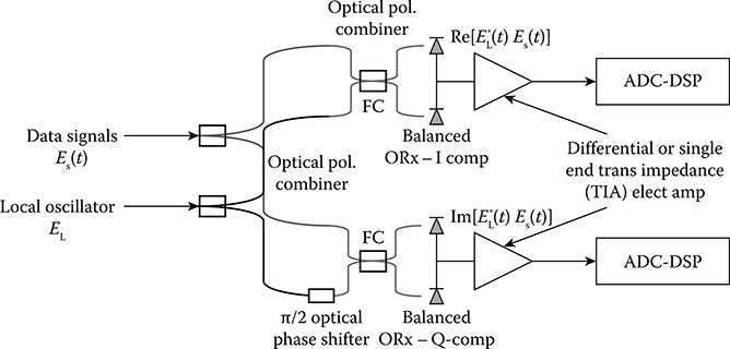
FIGURE 14.18 Schematic of a coherent receiver using balanced detection techniques for I–Q component phase and amplitude recovery, incorporating DSP and ADC.
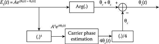
FIGURE 14.19 Schematic of a QPSK coherent receiver.
When the received signal is raised to the quadratic power, the phase of the signal disappears because ej4μs(t) = 1 for DQPSK, whose states are 0, π/2, π, 3π/2, 2π. The data phase is excluded, and the carrier phase can be recovered with its fluctuation with time. This estimation is computed using the DSP algorithm. The estimated carrier phase is then subtracted with the detected phase of the signal to give only the phase states of the signals as indicated in the diagram. This is a feed-forward (FF) phase estimation, and most suitable for DSP implementation either off-line or in real time.
14.4.4 Carrier Recovery in Polarization Division Multiplexed Receivers: a Case Study
Advanced modulation formats in combination with coherent receivers incorporating DSP subsystems enable high capacity and spectral efficiency [25,26]. PDM, QAM, and coherent detection are dominating the next-generation high-capacity optical networks since they allow information encoding in all the available degrees of freedom [27] with the same requirement of the OSNR. The coherent technique is homodyne or intradyne mixing of the signal carrier and the LO. However, as just mentioned, a major problem in homodyne coherent receiver is the CR, so that matching between the channel carrier and the LO can be achieved to maximize the signal amplitude and phase strength, and hence the SNR in both amplitude and phase planes. This section illustrates an experimental demonstration of the CR of a PDM-QPSK, transmission scheme carrying 100 Gbits/s per wavelength channel, including two polarized modes (H: horizontal; V: vertical) of the linear polarized mode in SSMF—that is, 28 GSy/s × 2 (2 bits/symbol) × 2 (polriazated channels) using some advanced DSP algorithms, especially the Viterbi-Viterbi (V-V) algorithm with MLSE nonlinear decision feedback procedures [28].
Feed-forward carrier phase estimation (FFCPE) [29] has been commonly considered as the solution for this problem. The fundamental operational principle is to assume a time invariant of the phase offset between carrier and local laser during N (N > 1) consecutive symbol periods.
In coherent optical systems using tunable lasers, the maximum absolute FO can vary by 5 GHz. To accommodate such a large FO, coarse digital frequency estimation (FDE) and recovery (FDR) techniques [30,31] can be employed to limit the FO to within an allowable range, so that phase recovery can be implemented/managed using fine FFCPE and fine feed-forward carrier phase recovery (FFCPR) techniques [32]. The algorithm presented in Ref. [22], the so-called “differential Viterbi” (DiffV), estimates phase difference between two successive complex symbols. This method enables the estimation of large FO of multiple phase shift keying (M-PSK)-modulated signals up to ± fs/(2M), where fs stands for the symbol rate frequency. It is possible to estimate larger FOs using the technique presented in Ref. [6], which generates insignificant estimation errors that can be handled by FFCPE and FFCPR. However, FFCPE, or “Viterbi and Viterbi” (V-V), would not perform well when the absolute residual FO at the input of the estimation circuit is larger than ± fs/(2MN). This problem becomes more serious when the laser frequency oscillates.
An algorithm for coupling carrier phase estimations in polarization division multiplexed (PDM) systems is presented in Ref. [33]. The algorithm requires two loop filters, and the coupling factor should be carefully selected. In the following section, an enhanced CR concept covering large FO and enabling almost zero residual FO for the V-V CPE is discussed. Also, a novel polarization coupling algorithm with reduced complexity is extracted from the work in Ref. [20].
14.4.4.1 FO Oscillations and Q Penalties
Figure 14.20 shows the typical DSP of medium complexity for coherent PDM optical transmission systems. CD and polarization effects are compensated in CD and MIMO blocks, respectively. The DV FE is realized in the microcontroller (MC). Several thousands of data sequences are periodically loaded to the microcontroller that calculates the FO. A small bandwidth of the estimation loop delivers only averaged FO value to the CMOS ASIC part. However, long-time experimental tests with commercially available lasers, for example, the EMCORE laser, show that laser frequency oscillations are sinusoidal with the frequency of 888 Hz in order to stabilize its central frequency by the use of a feedback control, and amplitude of more than 40 MHz (see Figure 14.21 for measured oscillation of the EMCORE external cavity laser as LO). This oscillation is created by the vibration of the external reflector—a grating surface, so that the cavity can be stabilized. The mean offset is close to 300 MHz. Therefore, the DiffV enables the averaging of the FO of 300 MHz, while the residual offset of ±50 MHz is compensated by the V-V algorithm.
Penalties caused by residual offset of 50 MHz have been investigated for case of V-V CPE. Figure 14.22 shows the simulation values of the Q penalties versus V-V averaging window length (WL) for two scenarios under off-line data processing. In first case, we multiplexed 112 G PDM-QPSK channel with 12 10 G on–off keying (OOK) neighbors (10 and 100 G over a 1200 km link), while the second scenario included the transmission of eight 112 G PDM-QPSK channels (100 G WDM—1500 km link). Channel spacing was 50 GHz (ITU-grid). The FO was partly compensated with the residual offset of 50 MHz to check the V-V CPR performance. Three values of LP have been checked: optimum launched power (LPopt), LPopt−1 dB (slightly linear regime), and LPopt+1 dB (slightly nonlinear regime). Maximum Q penalties of 0.9 dB can be observed, which strongly depend on the averaging window length parameter WL.

FIGURE 14.20 Typical DSP structure in PDM coherent receivers including a low-speed processor and high-speed DSP system. CPE = carrier phase estimation, MIMO = multiple input multiple output, CPR = carrier phase recovery, FR = frequency recovery, CD = chromatic dispersion.
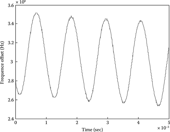
FIGURE 14.21 Laser frequency oscillation of EMCORE external cavity laser as measured from an external cavity laser.

FIGURE 14.22 Penalties of V-V CPR with a residual FO of 50 MHz.
14.4.4.2 Algorithm and Demonstration of Carrier Phase Recovery
A robust FFCPE and FFCPR with a polarization coupling circuit is shown in Figure 14.23. The FFCFE and FFCPR are developed for the recourses of the V-V, and, by simple recourses reallocation, an enhanced CR is obtained. The proposed method is designed to maximize CR performance with a moderate realization complexity. The method consists of four main parts: (1) coarse carrier frequency estimation by processing in slow-speed DSP subsystems (indicated by microcontroller) and recovery (CCFE-R), (2) feedback carrier frequency estimation and recovery (FBCFE-R, light gray lines in Figure 14.23), (3) X–Y phase offset estimation and compensation (H-V [or X–Y]-POE-C, gray line in Figure 14.23), and (4) joint H-V feed-forward carrier phase estimation and recovery (JFF-CPE-R).
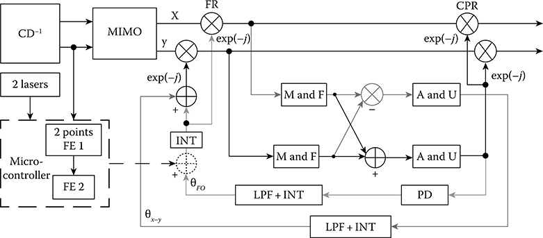
FIGURE 14.23 Modified structure of algorithms for CR. M&F = Mth power operation and averaging filter; A&U = arctan and unwrapping; PD = phase difference calculation; LPF = low-pass filter; INT = integrator. (Extracted from D.-S. Ly-Gagnon et al., Lightwave Technol., Vol. 24, pp. 12–21, 2006.)
The M-F block conducts the Mth power operation and averaging in case of the MPSK modulation format [6]. For the K-QAM signal, the M constellation points on the ring with a specific radius may be selected and used in Mth power block. More rings can be selected to improve the estimation procedure (e.g., inner and outer rings in 16QAM can be used). Therefore, the use of the method is not limited to PSK schemes.
Large FO [> ± fs/(2MN)] can be estimated by the method presented in Ref. [31] (denoted by FE1 in Figure 14.23), which can estimate the FO within ±10 GHz (linear curve in case of 112 G PDMQPSK). A small amount of data is transferred into the microcontroller for calculating the coarse range of the FO. Depending on the FO estimation sign, one can superimpose certain FOs (e.g., 4 GHz) of opposite signs. Using a linear interpolation (FE2), the current FO can be estimated to an error within a few hundreds of MHz. Similarly, depending on available electrical bandwidth and the receiver structure, the compensation of such a large FO can be conducted either in CMOS ASIC or by controlling the frequency of LO, commonly an ECL.
The residual FO after CCFE and CCFER may have values of several hundred MHz plus 50 MHz generated by low processing speeds and laser frequency oscillations. The FBCFE estimates the residual frequency that is compensated for by the CFR feedback loop. The frequency estimation in the range of FBCFE&R is ± fs/(2MN) due to its implementation based on the DiffV algorithm.
The FBCFE&R compensates almost the total FO. The residual FO and finite laser linewidth influence can be compensated for by the JFF-CPE&R. This operation can be supported by coupling the carrier estimations from both polarized channels. Prior to the coupling of estimations, both X and Y constellations are aligned using the X–Y-POE&C, and the phase difference between adjacent outputs of the lower unwrapping block can then be used for alignment. It is sufficient to rotate the Y polarization for the constellation angle mismatch.
The algorithm employing MIMO and V-V CPE is compared with the CR as presented in Figure 14.22, in which the uncompensated FO after the MIMO block is set to 50 MHz to simulate a realistic scenario. The measured FO after the MIMO is around 300 MHz. All data processing algorithms are done block-wise with parallelization of 64 symbols per block, and a realistic processing delay is added [20].
Figure 14.24 shows the gain in the quality factor Q for the two measurement cases. Since the FO is recovered by the feedback CR, the penalties shown in Figure 14.22 are completely compensated, with an additional gain coming from the estimations of coupling.
The 10 and 100 G hybrid off-line optical transmissions with homodyne coherent reception experiments are used to demonstrate the convergence of the feedback loops of the modified algorithm shown in Figure 14.23. As shown in Figure 14.25, the FO of 327 MHz can be acquired after 3.4 μs, or 1500 blocks of processing [20]—the steady state of the plateau region. The X–Y constellation offset is acquired after 3000 blocks due to the demand for correct FO compensation. The estimated X–Y phase offset is 0.8 rad. The CR can cope with a laser frequency oscillation of 36 MHz. Acquisition and tracking times are shown in Figure 14.26. The CR is able to track the laser frequency changes after 100 ms. Note that a feedback loop can cause delay between real oscillations and estimation (delay between two lines in Figure 14.26, hence resulting in some penalties).
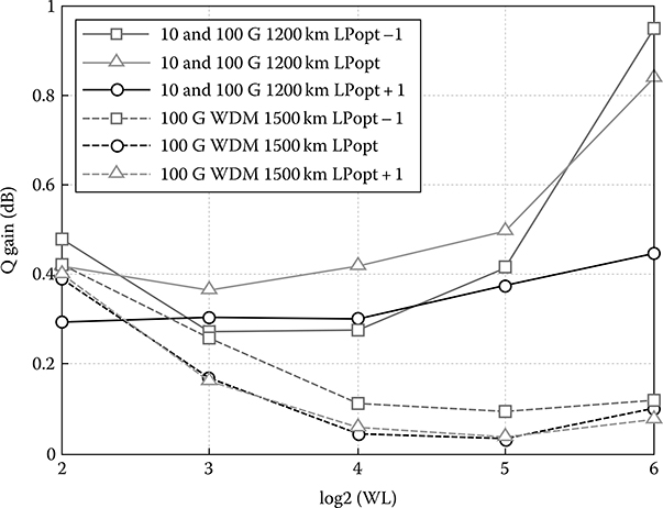
FIGURE 14.24 CR Q gain.

FIGURE 14.25 10 G hybrid off-line experiments LOFO and X–Y phase offset estimation by FO variation with respect to the number of blocks. FO = frequency offset—vertical axis.
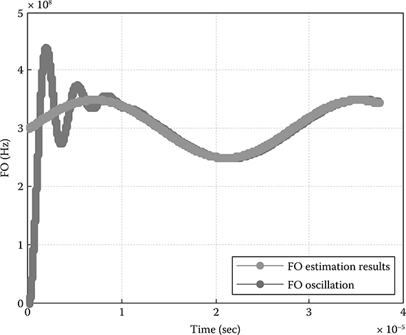
FIGURE 14.26 36 KHz oscillation variation of the laser frequency.
The high precision CR is achieved by the use of the V-V circuits under appropriate allocation and connections. Using feedback and feed-forward CR, significant improvements can be achieved. Laser FO can be compensated by complex circuit design and appropriate parameter selection. The ideal coupling of estimations coming from two polarizations further enhance CR performance with less complexity.
14.4.4.3 Modified Gardner Phase Detector for Nyquist Coherent Optical Transmission Systems
This section describes a timing recovery scheme based on a Gardner phase detector [34] performing excellently in spectrally efficient Nyquist coherent optical systems. Good clock tone performance can be obtained for QAM modulation formats, with the ROF values close to null.
14.4.4.3.1 Motivation
The link traffic can be increased by deploying more fibers, using L band, more efficient IP packaging, dynamic networking, and so on. Also, the spectral efficiency can be improved by applying higher-order modulation formats and efficient spectral shaping. Modulation formats and baud rates should be flexible in future elastic optical networks. In such scenarios, the network management will be able to select the best transmission scenario, depending on the link quality. It requires universal timing recovery, covering most modulation formats of interest. Most commercial timing recovery algorithms are designed for systems using non-return-to-zero and return-to-zero pulse shapes whose spectrums allow the generation of a spectral component at symbol frequency using the simplest nonlinear operations (squaring, rectifying, samples multiplication, etc.) or logical operations (early–late detectors). Several timing recovery candidates for high-speed optical coherent systems are discussed in Ref. [35]. However, in very dense WDM optical systems using Nyquist signaling with very small ROF values, most of the published timing algorithms failed. For example, a very famous square and filter algorithm [36] completely fails for the ROF value equal to zero. A phase detector (PD) described in Ref. [37], the so-called Gardner phase detector (GPD), is very effective in non-Nyquist systems, and can be realized in time domains with acceptable hardware complexity. This detector also fails at small ROF values. The fourth-power law PD (4PPD) presented in Ref. [37] can deal with small ROF values. This solution requires a carefully designed bandpass filter that can be replaced by a filter realized in the frequency domain. Due to PMD effects, the direct implementation of this method before PMD compensation is quite difficult. We propose an improved version of the Gardner PD having lower complexity than the 4PPD. The modified Gardner PD (MGPD) is independent of modulation formats and performs well in the most extreme transmission scenarios, with ROF close and equal to zero.
14.4.4.3.2 Timing Recovery
In coherent optical receivers, linear filters are employed to compensate for deterministic linear channel distortions such as residual CD and PMD. Timing/clock recovery, CR, nonlinear effects compensation, optical performance monitoring, differential decoding, forward error correction, and many other modules are also integral parts of the receiver. A microcontroller is responsible for slow-speed operations such as CD estimation, laser frequency control, controlling analog amplifiers, and so on. The clock tone can be characterized via several parameters [38]: timing error detector characteristics (TEDC), maximum of TEDC (TEDCMAX), peak-to-peak jitter (Jitterpp), and so on. Only the closed loop simulation of the considered transmission scenario can fully characterize timing performance. Timing recovery can be done either before or after PMD compensation. The Godard PD realization in the frequency domain before PMD compensation is shown in Figure 14.27. After CD compensation (CD−1 blocks), the signal is processed by a state-of-polarization (SOP) modifier to improve the clock quality. The SOP modifier is the unavoidable block that solves problems caused by PMD negative effects [39, 40 and 41].
In practical Nyquist systems, a raised-cosine filter is used to generate Nyquist pulses. Due to the effects of white noise, the RRC filters at the transmitter and receiver sides are often used in simulations and experiments. We simulated the system shown in Figure 14.27 for QPSK (4QAM) case at the energy per bit to noise power spectral density ratio (Eb/N0), equal to 3 dB (20% redundancy soft FEC threshold). TEDC for ROF values between 0 and 1 are shown in Figure 14.28. The clock tone drops at small ROF values and vanished completely for ROF = 0.
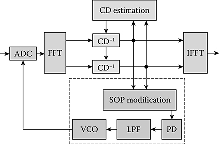
FIGURE 14.27 Implementation of Godard PD.
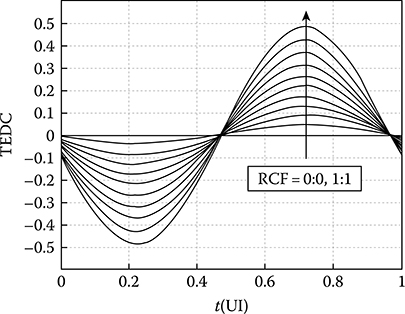
FIGURE 14.28 GPD TEDC; 4QAM; Eb/N0 = 3 dB.
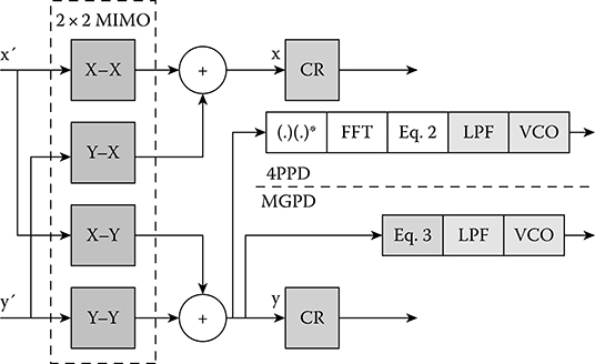
FIGURE 14.29 Implementation 4PPD and MGPD.
14.4.4.3.3 Algorithm Description
Since PDs based on the square and filter method fail for small ROF values, we can investigate the 4PPD and MGPD performance. Their implementations after PMD compensation are shown in Figure 14.29. Four complex filters are usually designed to work with two samples per symbol and to output only one sample. In our schematic, two filters, X–Y and Y–Y, are designed to output two samples per symbol. Therefore, only y output is used for timing extraction (two samples are required). The squared signal z = yy*[Z = fft(z)] is processed using blocks-generating outputs
The 4PPD requires FFT block (or a time domain FIR filter with an additional squarer). The MGPD consists of the squarer and the real-input Gardner PD. Apparently, the MGPD is less complex than the 4PDD. Since both PDs behave similarly, we continue with MGPD characterization. The implementation of 4PPD and MGPD is by using the experimental setup shown in Figure 14.30.
14.4.4.3.4 Simulation and Experimental Results
In all simulations, we assume a static 2 × 2 MIMO FIR filter whose coefficients are known in advance and do not vary over time. Eb/N0 was varied starting from values close to 20% soft FEC thresholds (Eb/N0,FEC) for the following modulation formats: 4QAM (3 dB), 16QAM (6 dB), and 64QAM (10 dB). TEDC of 4QAM versus ROF is presented in Figure 14.31. Clock tone is high at small ROF values, while high ROF destroys timing information. Sensitivity to ROF for different modulation formats is shown in Figures 14.32 and 14.33 (Eb/N0 = Eb/N0,FEC). Critical ROF value (low TEDCMAX) is lower for higher-level modulation formats. Anyhow, all of them perform well at small ROF values. TEDCMAX values over Eb/N0 region of interest are shown in Figure 14.7. The 16QAM and 64QAM formats are almost insensitive to Eb/N0 variations, while in case of 4QAM the TEDCMAX value is doubled at maximum Eb/N0 value. Estimating clock tone quality only via TEDCMAX is not valid. Closed loop simulation with carefully adjusted parameters can tell more about the considered scheme. Therefore, we averaged PD output at the equilibrium point by the use of a sliding window filter of length 1024 (symbols). Simulated peak-to-peak jitter over 107 symbols is presented in Figure 14.34. Maximum jitter was around 3% of unit interval (UI), which causes negligible BER performance degradation at Eb/N0,FEC values for all modulation formats. It is thus experimentally investigated here, with the timing algorithm using a setup shown in Figure 14.30. Using DSP, we generated the Nyquist signal including transmitter imperfections compensation. Due to the limited bandwidth of analog devices, DAC crosstalk, and time-varying unpredictable effects, we were not able to generate very accurate ROF values. Results for the GPD and MGPD are presented in Figures 14.35 and 14.36, respectively. One can observe very good agreement between simulations and experiments for both PDs. The proposed PD showed the best performance for small ROF values, while the GPD performance is better at high ROF values.
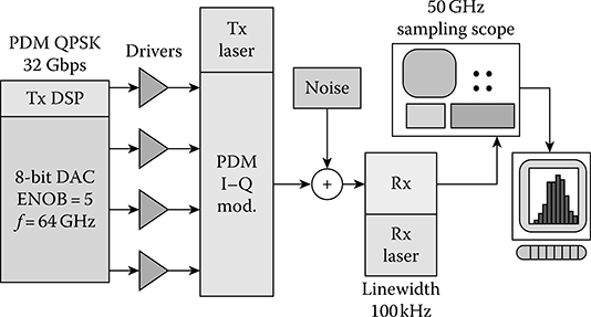
FIGURE 14.30 Experiment setup.
FIGURE 14.31 MGPD TEDC; 4QAM; Eb/N0 = 3 dB.

FIGURE 14.32 MGPD TEDCMAX versus ROF.
FIGURE 14.33 MGPD. TEDCMAX at ROF = 0 (MGPD).

FIGURE 14.34 Jitter peak-to-peak at ROF = 0 (MGPD).

FIGURE 14.35 Experiment-GPD TEDCMAX.

FIGURE 14.36 Experiment-MGPD TEDCMAX.
14.5 Systems Performance of Mlse Equalizer–msk Optical Transmission Systems
14.5.1 MLSE Equalizer for Optical MSK Systems
14.5.1.1 Configuration of MLSE Equalizer in Optical Frequency Discrimination Receiver
Figure 14.37 shows the block diagram of a narrowband filter receiver integrated with NLEs for the detection of 40 Gbps optical MSK signals. The structure and operation of the MSK transmitter have been described in Chapter 3. MSK employs 2 bits/symbol modulation as in the case of QPSK but with continuous phase change at the transition between the bit periods. Continuous phase change can lead to very effective frequency spectrum and hence MSK looks like FDM with the two frequencies are separated by 1/4T. Hence, when the frequency difference between states equals a quarter of the bit rate, the minimum distance between them so that the channel states can be recovered with minimum ISI, then the two frequency states are orthogonal, and then the modulation is termed as minimum shift keying, or MSK.
In the reception of MSK channels, two narrowband filters can be used to discriminate the upper sideband (USB) and lower sideband (LSB) channel frequencies that correspond to the logical “1” and “0” transmitted symbols, respectively. A constant optical delay line that is easily implemented in integrated optics is introduced on one branch to compensate for any differential group delay td = 2πfdβ2 L between f1 and f2 where fd = f−1 − f2 = R/2, β2, represents group velocity delay (GVD) parameter of the fiber, and L is the fiber length, as described in Chapter 2. Alternatively, deskewing can be implemented in the digital domain to compensate for this delay difference. If the differential group delay is fully compensated, the optical lightwaves in two paths arrive at the photodiodes simultaneously. The outputs of the filters are then converted into electrical domain through the photodiodes. These two separately detected electrical signals are sampled before being fed as the inputs to the NLE.

FIGURE 14.37 Block diagram of narrowband filter receiver integrated with nonlinear equalizers for the detection of 40 Gbps optical MSK signals.
It is noted here that the MSK reception system described here can be a self-homodyne detection or a coherent detection with the signal channel employed as the LO. Alternatively, the receiver subsystem can employ the coherent detection technique in that an optical LO oscillator is used to mix with the signals so that the resultant power level can be boosted up and hence the increase of the sensitivity of the receiver.
14.5.1.2 MLSE Equalizer with Viterbi Algorithm
At epoch k, it is assumed that the effect of ISI on an output symbol of the FSM ck is caused by both executive δ pre-cursor and δ post-cursor symbols on each side. First, a state trellis is constructed with 2δ states for both detection branches of the optical frequency discrimination receiver (OFDR). A lookup table per branch corresponding to the symbols “0” and “1” transmitted and containing all the possible 22δ states of all 11 symbol-length possible sequences is constructed by sending all the training sequences incremented from 1 to 22δ.
The output sequence c(k) = f(bk, bk−1, …, bk−2δ −1) = (c1, c2, ..., c2δ;) is the nonlinear function representing the ISI caused by the δ adjacent pre-cursor and post-cursor symbols of the optical fiber FSM. This sequence is obtained by selecting the middle symbols ck of 2δ possible sequences with length of 2δ + 1 symbol intervals.
The samples of the two filter outputs at epoch , i = 1, 2 can be represented as , i = 1,2. Here, and represent the amplified spontaneous emission (ASE) noise and the electrical noise, respectively.
In linear transmission of an optical system, the received sequence yn is corrupted by ASE noise of the optical amplifiers, nASE, and the electronic noise of the receiver, nE. It has been proven that the calculation of branch metric and hence state metric is optimum when the distribution of noise follows the normal/Gaussian distribution—that is, the ASE accumulated noise and the electronic noise of the reception subsystem are collectively modeled as samples from Gaussian distributions. If the noise distribution departs from the Gaussian distribution, the minimization process is suboptimum.
The Viterbi algorithm subsystem is implemented on each detection branch of the OFDR. However, the MLSE with Viterbi algorithm may be too computationally complex to be implemented at 40 Gbps with the current integration technology. However, there have been commercial products available for 10 Gbps optical systems. Thus, a second MLSE equalizer using techniques of reduced-state template matching is presented in the following section.
In an optical MSK transmission system, narrowband optical filtering plays the main role in shaping the noise distribution back to the Gaussian profile. The Gaussian profile noise distribution is verified in Figure 14.38. Thus, branch metric calculation in the Viterbi algorithm, which is based on minimum Euclidean distance over the trellis, can achieve the optimum performance. Also, the computational effort is less complex than ASK or DPSK systems due to the issue of non-Gaussian noise distribution.
FIGURE 14.38 Noise distribution following Gaussian shape due to narrowband optical filtering.
14.5.1.3 MLSE Equalizer With Reduced-State Template Matching
The modified MLSE is a single-shot template-matching algorithm. First, a table of 22δ+1 templates, gk, k = 1, 2, …, 22δ+1, corresponding to the 22δ+1 possible information sequences, I k, of length 2δ+1 is constructed. Each template is also a vector of size 2δ+1, which is obtained by transmitting the corresponding information sequence through the optical channel and obtaining the 2δ+1 consecutive received samples. At each symbol period, n, the sequence, În, with the minimum metric is selected as . The middle element of the selected information sequence is then output as the nth decision, În—that is, În = In(δ + 1). The minimization is performed over the information sequences, Ik, which satisfy the condition that the δ−2 elements are equal to the previously decoded symbols În−δ, In−(δ−1), …În−2, and the metric, m(Ik, rn), is given by m(Ik, rn ) = {w· (gk − rn}T{w·(gk − rn)}, where w is a weighting vector that is chosen carefully to improve the reliability of the metric. The weighting vector is selected so that, when the template is compared with the received samples, less weighting is given to the samples further away from the middle sample. For example, we found through numerical results that a weighting vector with elements w(i) = 2−|i−(δ + 1)|, i = 1, 2, …, 2δ+1 gives good results. Here, ∙ represents Hadamard multiplication of two vectors, (.)T represents transpose of a vector, and |.| is the modulus operation.
14.5.2 MLSE Scheme Performance
14.5.2.1 Performance of MLSE Schemes in 40 Gbps Transmission Systems
Figure 14.39 shows the simulation system configuration used for the investigation of the performance of both the preceding schemes when used with the narrowband optical Gaussian filter receiver for the detection of noncoherent 40 Gbps optical MSK systems. The input power into fiber (P0) is −3 dBm, which is much lower than the nonlinear threshold power. The EDFA2 provides 23 dB gain to maintain the receiver sensitivity of −23.2 dBm at BER = 10−9. As shown in Figure 14.39, the optical received power (PRx) is measured at the input of the narrowband MSK receiver, and the OSNR is monitored to obtain the BER curves for different fiber lengths. The length of SSMF is varied from 48 to 60 km in steps of 4 km to investigate the performance of the equalizers to the degradation caused by fiber cumulative dispersion. The narrowband Gaussian filter with the time bandwidth product of 0.13 is used for the detection filters.

FIGURE 14.39 Simulation setup for performance evaluation of MLSE and modified MLSE schemes for detection of 40 Gbps optical MSK systems.
TABLE 14.2
Key Simulation Parameters Used in The MLSE MSK Modulation Format
| Input power: P0 = −3 dBm | Narrowband Gaussian filter: B = 5.2 GHz or BT = 0.13 |
| Operating wavelength: λ = 1550 nm | Constant delay: td = |2πfDβ2L| |
| Bit rate: R = 40 Gbps | Preamp. EDFA of the OFDR: G = 15 dB and NF = 5 dB |
| SSMF fiber:|β2 | = 2.68e−26 or |D | = 17 ps/nm/km | id= 10 nA |
| Attenuation: α = 0.2 dB/km | Neq= 20 pA/(Hz)1/2 |
Electronic noise of the receiver can be modeled with the equivalent noise current density of electrical amplifier of 20 and dark current of 10 nA. The key parameters of the transmission system are given in Table 14.2.
The Viterbi algorithm used with the MLSE equalizer has a constraint length of 6 (i.e., 25 number of states) and a trace-back length of 30. Figure 14.40 shows the BER performance of both NLEs plotted against the required OSNR. The BER performance of the optical MSK receiver without any equalizers for 25 km SSMF transmission is also shown in Figure 14.40 for quantitative comparison. The numerical results are obtained via Monte Carlo simulation (triangular markers as shown in Figure 14.40) with the low BER tail of the curve linearly extrapolated. The OSNR penalty (at BER = 10−9) versus residual dispersion corresponding to 48, 52, 56, and 60 km SSMF are presented in Figure 14.41. The MLSE scheme outperforms the modified MLSE schemes, especially at low OSNR. In the case of 60 km SSMF, the improvement at BER = 10−9 is approximately 1 dB, and in the case of 48 km SSMF, the improvement is about 5 dB. In case of transmission of 52 km and 56 km SSMF, MLSE with Viterbi algorithm has 4 dB gain in OSNR compared to the modified scheme. With residual dispersion at 816, 884, 952, and 1020 ps/nm, at a BER of 10−9, the MLSE scheme requires 12, 16, 19, and 26 dB OSNR penalty, respectively, while the modified scheme requires 17, 20, 23, and 27 OSNR, respectively.
14.5.2.2 Transmission of 10 Gbps Optical MSK Signals Over 1472 km SSMF Uncompensated Optical Links
Figure 14.42 shows the simulation setup for 10 Gbps transmission of optical MSK signals over 1472 km SSMF. The receiver employs an optical narrowband frequency discrimination receiver integrated with a 1024-state Viterbi-MLSE postequalizer. The input power into the fiber (P0) is −3 dBm lower than the fiber nonlinear threshold power. The optical amplifier EDFA1 provides an optical gain to compensate the attenuation of each span completely. The EDFA2 is used as a noise-loading source to vary the required OSNR. The receiver electronic noise is modeled with equivalent noise current density of the electrical amplifier of 20 and dark current of 10 nA for each photodiode. A narrowband optical Gaussian filter with two-sided bandwidth of 2.6 GHz (one-sided BT = 0.13) is optimized for detection. A back-to-back (BTB) OSNR = 8 dB is required for BER at 10−3 for each branch. The correspondent received power is −25 dBm. This low OSNR is possible due to the large suppression of noise after being filtered by narrowband optical filters. A trace-back length of 70 is used in the Viterbi algorithm. Figure 14.42 shows the simulation results of BER versus the required OSNR for 10 Gbps optical MSK transmission over 1472 and 1520 km SSMF uncompensated optical links with one, two, and four samples per bit, respectively. A 1520 km SSMF with one sample per bit is seen as the limit for the 1024-state Viterbi algorithm due to the slow roll-off and the error floor. However, two and four samples per bit can obtain error values lower than the FEC limit of 10−3.

FIGURE 14.40 Performance of modified Viterbi-MLSE and template-matching schemes, BER versus OSNR.
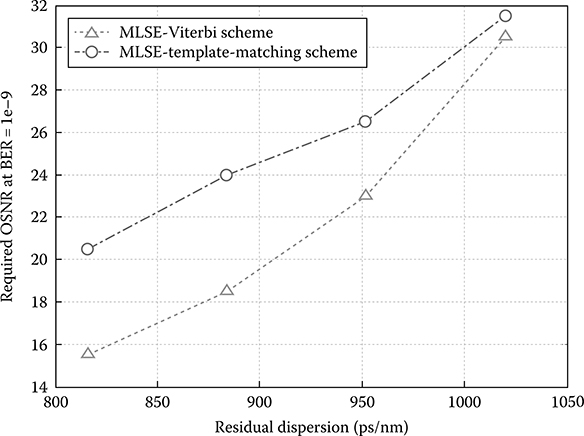
FIGURE 14.41 Required OSNR (at BER = 1e−9) versus residual dispersion in Viterbi-MLSE and template-matching MLSE schemes.
Thus, 1520 km SSMF transmission of 10 Gbps optical MSK signals can reach the error-free detection with the use of a high-performance FEC. In case of 1472 km SSFM transmission, the error events follow a linear trend without sign of error floor and, therefore, error-free detection can be comfortably accomplished.
Figure 14.43 also shows the significant improvement in OSNR of two and four samples per bit over one sample per bit counterpart with values of approximately 5 and 6 dB, respectively. In terms of OSNR penalty at BER of 1e−3 from BTB setup, four samples per bit for 1472 and 1520 km transmission distance suffers 2 and 5 dB penalty, respectively.

FIGURE 14.42 Simulation setup for transmission of 10 Gbps optical MSK signals over 1472 km SSMF with MLSE-Viterbi equalizer integrated with the narrowband optical filter receiver.

FIGURE 14.43 BER versus required OSNR for transmission of 10 Gbps optical MSK signals over 1472 and 1520 km SSMF uncompensated optical link.
14.5.2.3 Performance Limits of Viterbi-MLSE Equalizers
The performance limits of the Viterbi-MLSE equalizer to combat the ISI effects are investigated against various SSMF lengths of the optical link. The number of states used in the equalizer is incremented according to this increase and varied from 26 to 210. This range was chosen as reflecting the current feasibility and future advance of electronic technologies that can support high-speed processing of the Viterbi algorithm in the MLSE equalizer. In addition, these numbers of states also provide feasible time for simulation.
In addition, one possible solution to ease the requirement of improving the performance of the equalizer without increasing much the complexity is by multisampling within one-bit period. This technique can be used by interleaving the samplers at different times. Although a greater number of electronic samplers are required, they only need to operate at the same bit rate as the received MSK electrical signals. Moreover, it will be shown later on that there is no noticeable improvement with more than two samples per bit period. Hence, the complexity of the MLSE equalizer can be affordable while improving the performance significantly.
Figure 14.44 shows the simulation setup for 10 Gbps optical MSK transmission systems with lengths of uncompensated optical links varying up to 1472 km SSMF. In this setup, the input power into fiber (P0) is set to be −3 dBm, thus avoiding the effects of fiber nonlinearities. The optical amplifier EDFA1 provides an optical gain to compensate for the attenuation of each span completely. The EDFA2 is used as a noise-loading source to vary the required OSNR values. Moreover, a Gaussian filter with two-sided 3 dB bandwidth of 9 GHz (one-sided BT = 0.45) is utilized as the optical discrimination filter because this BT product gives the maximized detection eye openings. The receiver electronic noise is modeled with equivalent noise current density of the electrical amplifier of 20 and a dark current of 10 nano-Ampere (nA) for each photodiode. A BTB OSNR = 15 dB is required for a BER of 10−4 on each branch, and the correspondent receiver sensitivity is −25 dBm. A trace-back length of 70 samples is used for the Viterbi algorithm in the MLSE equalizer. Figures 14.44, 14.45 and 14.46 show the BER performance curves of 10 Gbps OFDR-based MSK optical transmission systems over 928, 960, 1280, and 1470 km SSMF uncompensated optical links for different number of states used in the Viterbi-MLSE equalizer. In these figures, the performance of Viterbi-MLSE equalizers is given by the plot of the BER versus the required OSNR for several detection configurations: balanced receiver (without incorporating the equalizer), the conventional single-sample-per-bit sampling technique, and the multisample-per-bit sampling techniques (two and four samples per bit slot). The simulation results are obtained by the Monte Carlo method.
The significance of multisamples per bit slot in improving the performance for MLSE equalizer in cases of uncompensated long distances is shown. It is found that the tolerance limits to the ISI effects induced from the residual CD of a 10 Gbps MLSE equalizer using 26, 28, and 210 states are approximately equivalent to lengths of 928, 1280, and 1440 km SSMF, respectively. The equivalent numerical figures in the case of 40 Gbps transmission are corresponding to lengths of 62, 80, and 90 km SSMF, respectively.

FIGURE 14.44 Simulation setup of OFDR-based 10 Gbps MSK optical transmission for study of performance limits of MLSE-Viterbi equalizer.

FIGURE 14.45 Performance of 64-state Viterbi-MLSE equalizers for 10 Gbps OFDR-based MSK optical systems over (a) 960 km and (b) 928 km SSMF uncompensated links.

FIGURE 14.46 Performance of 256-state Viterbi-MLSE equalizer for 10 Gbps OFDR-based MSK optical systems over 1280 km SSMF uncompensated links.
In the case of 64 states over 960 km SSMF uncompensated optical links, the BER curve encounters an error floor that cannot be overcome even by using high-performance FEC schemes. However, at 928 km, the linear BER curve indicates the possibility of recovering the transmitted data with the use of high-performance FEC. Thus, for 10 Gbps OFDR-based MSK optical systems, a length of 928 km SSMF can be considered as the transmission limit for the 64-state Viterbi-MLSE equalizer. Results shown in Figure 14.46 suggest that the length of 1280 km SSMF uncompensated optical link is the transmission limit for the 256-state Viterbi-MLSE equalizer when incorporating with OFDR optical front end. It should be noted that this is achieved when using the multisample-per-bit sampling schemes.
It is observed from Figure 14.47 that the transmission length of 1520 km SSMF with one sample per bit is seen as the limit for the 1024-state Viterbi algorithm due to the slow roll-off and the error floor. However, two and four samples per bit can obtain error values lower than the FEC limit of 10−3. Thus, 1520 km SSMF transmission of 10 Gbps optical MSK signals can reach the error-free detection with use of a high-performance FEC. In case of 1472 km SSFM transmission, the error events follow a linear trend without sign of error floor, and, therefore, error-free detection can be achieved. Figure 14.47 also shows the significant OSNR improvement of the sampling techniques with two and four samples per bit compared to the single-sample-per-bit counterpart. In terms of OSNR penalty at a BER of 1e−3 from BTB setups, four samples per bit for 1472 and 1520 km transmission distance suffers 2 and 5 dB penalty, respectively.
It is found that, for incoherent detection of optical MSK signals based on the OFDR, an MLSE equalizer using 24 states does not offer better performance than the balanced configuration of the OFDR itself; that is, the uncompensated distance is not over 35 km SSMF for 40 Gbps or 560 km SSMF for 10 Gbps transmission systems, respectively. It is most likely that, in this case, the severe ISI effect caused by the optical fiber channel has spread beyond the time window of five bit slots (two pre-cursor and two post-cursor bits), the window that a 16-state MLSE equalizer can handle. Thus, it is necessary that the number of taps or states of MLSE cover the full length of the dispersive pulse.
The trace-back length used in the investigation is chosen to be 70, which guarantees the convergence of the Viterbi algorithm. The longer the trace-back length, the larger the memory that is required. With state-of-the-art technology for high storage capacity nowadays, memory is no longer a big issue. Very fast processing speeds at 40 Gbps operations hinder the implementation of 40 Gbps Viterbi-MLSE equalizers at the mean time. Multisample sampling schemes offer an exciting solution for implementing fast signal processing processes. This challenge may also be overcome in the near future together with the advance of the semiconductor industry. At present, the realization of Viterbi-MLSE equalizers operating at 10 Gbps has been commercially demonstrated [42].

FIGURE 14.47 Performance of 1024-state MLSE equalizer for 10 Gbps optical MSK signals versus the required OSNR over 1472 and 1520 km SSMF uncompensated optical link.
14.5.2.4 Viterbi-MLSE Equalizers for PMD Mitigation
Figure 14.48 shows the simulation test bed for the investigation of MLSE equalization of the PMD effect. The transmission link consists of a number of spans comprising 100 km SSMF (with D = +17 ps/(nm km), α = 0.2 dB/km) and 10 km DCF (with D = −170 ps/(nm km), α = 0.9 dB/km). Launched power into each span (P0) is −3 dBm. The EDFA1 has a gain of 19 dB, hence providing input power into the DCF to be −4 dBm, which is lower than the nonlinear threshold of the DCF. The 10 dB gain of EDFA2 guarantees the input power into next span unchanged with an average power of −3 dBm. An OSNR of 10 dB is required for receiver sensitivity at BER of 10−4 in case of back-to-back configuration. Considering the practical aspect and complexity, a Viterbi-MLSE equalizer for PMD equalization, and a small number of four-state bits, or effectively 16 states, were chosen for the Viterbi algorithm in the simulation study.
The performance of MLSE against the PMD dynamic of optical fiber is investigated. BER versus required OSNR for different values of normalized average differential group delay (DGD) <Δt> are shown in Figure 14.49. The mean DGD factor is normalized over one-bit period of 100 and 25 ps for 10 and 40 Gbps bit rates, respectively. The numerical studies are conducted for a range of values from 0 to 1 of normalized DGD <Δt>, which equivalently corresponds to the instant delays of up to 25 or 100 ps in terms of 40 and 10 Gbps transmission bit rate, respectively.

FIGURE 14.48 Simulation test bed for investigation of effectiveness of MLSE equalizer to PMD.

FIGURE 14.49 Performance of MLSE equalizer versus normalized <Δτ> values for one sample per bit.
The advantages of using multiple samples per bit over the conventional single sample per bit in MLSE equalizer are also numerically studied, and the Monte Carlo results for normalized DGD values of 0.38 and 0.56 are shown in Figures 14.50 and 14.51. However, the increase from two to four samples per bit does not offer any gain in the performance of the Viterbi-MLSE equalizer. Thus, two samples per symbol are preferred to reduce the complexity of the equalizer. Here, and for the rest of this chapter, multisamples per bit implies the implementation of two samples per symbol. Performance of MLSE equalizer for different normalized DGD values with two samples per bit is shown in Figure 14.52. From Figure 14.52, the important remark is that 16-state MLSE equalizer implementing two samples per symbol enables the optical MSK transmission systems achieving a PMD tolerance of up to one-bit period at BER = 10−4, with a required OSNR of 8 dB. This delay value starts introducing a BER floor, indicating the limit of the 16-state MLSE equalizer. This problem can be overcome with a high-performance FEC. However, the DGD mean value of 0.94 can be considered as the limit for an acceptable performance of the proposed MLSE equalizer without the aid of high-performance FEC. Figure 14.53 shows the required OSNR for MLSE performance at 10−4 versus normalized <Δt> values in configurations of balanced receiver, one sample per bit, and two samples per bit.
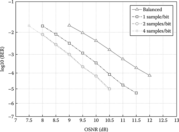
FIGURE 14.50 Comparison of MLSE performance for configurations of one, two, and four samples per bit, with normalized <Δτ> value of 0.38.
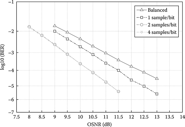
FIGURE 14.51 Performance of Viterbi-MLSE equalizer for configurations of one, two, and four samples per bit, with a normalized <Δτ> value of 0.56.
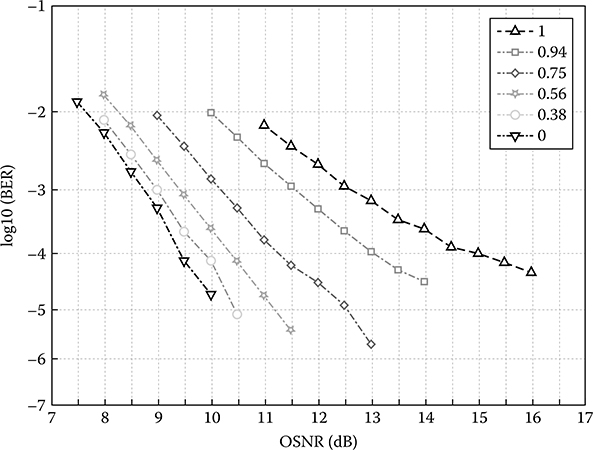
FIGURE 14.52 Performance of Viterbi-MLSE equalizer for different normalized <Δt> values with two and four samples per bit.
A balanced receiver, with no MLSE equalizer incorporated, requires an OSNR = 5 dB to obtain a BER = 10−4 when there are no effects of the PMD compared to the required OSNR of 3 and 1 dB in cases of one sample per bit and two samples per bit, respectively. The OSNR penalties for various normalized <Δt> values of the preceding three transmission system configurations are shown in Figure 14.54.
It can be observed that the OSNR penalties (BTB) of approximately 3 and 1 dB apply to the cases of balanced receiver and one sample per bit, respectively, with reference to the two samples per bit configuration. Another important remark is that the 16-state Viterbi-MLSE equalizer that implements two samples per bit enables the optical MSK transmission systems achieving a PMD tolerance of up to one-bit period at a BER of 10−4 with a power penalty of about 6 dB. Moreover, the best 2 dB penalty occurs at 0.75 for the value of normalized <Δt>. This result shows that the combination of OFDR-based MSK optical systems and Viterbi-MLSE equalizers, particularly with the use of multisample sampling schemes, was found to be highly effective in combating the fiber PMD dynamic impairment and better than the recently reported PMD performance for OOK and DPSK modulation formats [43].
14.5.2.5 Uncertainty and Transmission Limitation of the Equalization Process
The fundamental limitations of a quadratic phase media on the transmission speed are formulated in signal space for significant applications in signal equalization. These limitations are quantitatively derived for both coherent and incoherent optical systems. This section investigates the dispersive effect of optical fiber on the transmission speed of the media. The main effect of dispersion is pulse broadening (and frequency chirping) as the signal pulses propagate through the quadratic phase media. This causes ISI, thereby limiting the speed of transmission. There are various ways of mitigating the harmful effects of ISI. One way is to use optical fiber with antidispersive property to equalize the dispersion. In practice, this optical scheme reduces signal level and thus requires amplification. The amplifier introduces noise, which in turn limits the channel speed (Shannon’s information capacity theorem). Another way of combating ISI is by digital electronic equalization means, such as MLSE, which is applicable for both coherent and incoherent detection schemes [44, 45, 46, 47 and 48]. These reported results show clearly that there is a fundamental limit on the achievable transmission speed for a given fiber length.

FIGURE 14.53 Required OSNR for MLSE performance at 10−4 versus normalized <Δt> values in configurations of balanced receiver and one and two samples per bit.
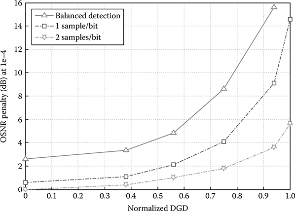
FIGURE 14.54 OSNR penalties of MLSE performance at 10−4 for various normalized <Δt> values in configurations of balanced receiver, single sample, and two samples per bit sampling schemes.
This section studies the limitation of quadratic phase channel, the single-mode optical fiber, in terms of signal space. The signal space is chosen so that it consists of binary signals in eight-bit block code. As the eight-bit symbols propagate down the quadratic phase channel, naturally the waveform patterns of the symbols would become less and less distinctive, and hence more and more difficult to discriminate between symbols. How do we quantify the detrimental effect of the quadratic phase channel? This system performance is approached entirely from a digital communications perspective, and the results so derived are the fundamental limit imposed by the quadratic phase channel (pure phase distortion but quadratic or square dependence of frequency by the linear dispersion). It is virtually independent of the detection scheme used. Two mechanisms that limit the transmission speed are explained. One is brought about by the finite time window available for detection. In all practical schemes, the decoder must decode each symbol within a finite time period. This requires the algorithm to be the least complex as possible. The other is brought about by not using the phase information for detection. Depending on the complexity of the detection scheme chosen, it is quite often that the phase information may be lost inadvertently when the optical signal is converted into the electrical signal. Another issue is the power consumption of the ASICs for implementation of digital algorithms for real-time applications. The more complex the algorithms are, the higher the number of digital circuits, and hence the more the power consumption. It is expected that all ASIC must consume less than 70 W in real-time processing.
14.6 Adaptive Joint CR and Turbo Decoding for Nyquist Terabit Optical Transmission in The Presence of Phase Noise
This section describes an adaptive joint CR and soft low-density parity check (LDPC) code turbo decoding (TD) scheme in the presence of nonlinear phase noise, proposed and experimentally verified with 1.9 dB coding gain in Nyquist Terabit PDM-DQPSK systems [49].
14.6.1 Motivation
Using Nyquist pulse shaping in Tbps transmission systems [50, 51 and 52] has recently attracted significant research interest, focusing on spectrally efficient ultra-high-capacity optical communications. This is especially important for systems employing fixed or flexible grid wavelength division multiplexing (WDM) grid. The performance of Nyquist coherent systems strongly depends on the capability of DSP algorithms. In combination with DSP, the advanced FEC codes such as LDPCs allow significant increasing transmission distance [53, 54 and 55].
The success of soft FEC decoding is often related to the quality of log-likelihood ratio (LLR) information, which is mainly related to additive white Gaussian noise (AWGN) channels. However, the noise statistics can be significantly influenced by the imperfect compensation of linear and nonlinear fiber channel impairments, the CR capability, the differential decoding (if employed), and efficiency of DSP algorithms [56,57]. The residual nonlinear phase noise induces substantial performance degradation.
In a previous work, soft differential decoding (SDD) and BCJR decoder performance have been investigated under AWGN channels, including analysis of the performance of quasi-cyclic LDPC (QC-LDPC) codes in differentially encoded 100 G optical transmission systems [44]. This section presents the optimization of CR and soft LDPC TD in practical Nyquist Terabit PDM-DQPSK systems in which the turbo decoder experiences severe performance degradation due to the residual nonlinear phase noise. To overcome this problem, adaptive joint CR and soft LDPC TD algorithm can be proposed. Utilizing probability density function (PDF) of CR output signal derived from a training sequence and post-FEC hard decision bits, the CR module adaptively mitigates more nonlinear phase noise. Furthermore, an associate LLR estimator provides more reliable LLR to turbo decoders. The adaptive scheme is proven to offer a significant system decoding gain in Tbps experimental platform.
14.6.2 Terabit Experiment Setup and Algorithm Principle
In our experiment, we have used 1T Nyquist transmitter (see Figure 14.55), consisting of four high-speed DAC with eight bit resolution (effective number of bits—ENOB equals 5.2—see ADC and DAC described in Chapter 3), a comb generator for subcarrier generation (10 channels; 10 × 128 G; channel spacing 33.3 GHz), ECL lasers of 100 KHz linewidth, two LiNbO3-based PDM I–Q modulators (MZMs), and optical filters/multiplexers. FEC-encoded Nyquist shaped data are loaded to four DACs. RRC pulses generated at the Tx output closely approached the rectangular spectral shape with an ROF α of 0.01. One of 10 subcarriers from the comb generator is filtered out by a wavelength selective switch (WSS). The other nine are modulated by MZM2 and further combined with the probed channel modulated by MZM1. The optical superchannel is then launched into the transmission system build of several spans. Each span consists of 75 km SSMF, a variable optical attenuator (VOA), and an EDFA. A preamplified Tektronix DP073304D coherent receiver records one of the channels with a sampling frequency of 50 GSa/s. The received signals are then processed off-line. In addition to the BTB case, two transmission scenarios are investigated: 1T superchannel transmission (1200 km link; no DCF; LP 1~4 dBm; the middle subcarrier was chosen as probe channel) and 1T/10 G-OOK hybrid transmission (800 km link with DCF; 50 GHz channel spacing between 10 G and 1T channel; subcarrier channel adjacent to the 10 G channel selected as probe). The DSP module compensates for skew, quadrature error, residual CD, PMD, and frequency and phase offset. The feed-forward carrier recovery (FF-CR) based on the Viterbi-Viterbi algorithm presented in Section 14.5 and also in Chapter 13, is used.
Figure 14.56 illustrates the adaptive joint CR and FEC principle, where PDF and LLR estimators are placed between the CR and FEC decoder. Pre-FEC BER and PDF are interactively estimated by two negative feedback paths, one between the training sequence bits and the post-DSP soft information, and the second between post-FEC hard decision bits and the soft information. Two types of 1T/10 G hybrid transmission PDF estimation results at the output of PDF and pre-FEC BER estimator are also inserted, as shown in Figure 14.56. In the first accumulate distribution approaches a Gaussian profile with the PDF side lobes indicating the cycle slip frequency. The two-dimensional “egg-shaped” PDF contour indicates the CR averaging effects. The estimated PDF profile and the CR soft outputs are then employed in the LLR estimator so as to generate LLR for the proposed FEC decoder. Simultaneously, the PDF estimator analyzes the distortion caused by the phase noise and the probability of cycle slips. Thence, feedback control signals are applied to the CR block that adaptively adjusts the CR averaging window length (dithering mode), so as to decrease the nonlinear phase noise negative effects. The PDF estimator can be realized in a microcontroller without difficulty due to the slow temporal variation of the phase noises.

FIGURE 14.55 Experimental setup platform for adaptive joint carrier recovery. Insert is the superchannel spectrum of 1 Tbps with probe channel filtered out.
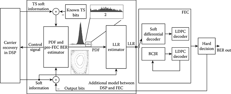
FIGURE 14.56 Adaptive joint carrier recovery and soft FEC decoding, two decoding schemes are applied in FEC block. TS = training sequence; pdf = probability density function.
Two decoding architectures are applied in the FEC block (see Figure 14.56)—SDD plus LDPC (SF) with ten iterations in LDPC decoder, and iterative TD investigated in Ref. [43] (BCJR plus SD-FEC) with ten iterations between LDPC and BJCR decoders. The BER was derived after the CR (pre-FEC BER) and after the FEC block (post-FEC BER).
The experimental data are first processed in the traditional way without the proposed technique. The BER of 1T BTB post-FEC under TD and SF are presented, respectively, as dotted and solid lines connecting, in Figure 14.57. The TD method outperforms the SF one by 2.2 dB at a BER of 1e−5. These improved performances are in much agreement with the simulation presented in Ref. [43]. These results are expected since the EDFA superimposed noise is the principal impairment in the BTB case without the influences of nonlinearity. The CR generates high-quality soft information to the turbo decoder, which reduces to a post-FEC BER of 1.12e−6 from a pre-FEC BER of 0.0161 with an OSNR of 11.5 dB and no cycle slips. However, the BCJR differential decoder almost doubles BER after the first run (BER = 0.0382). The corresponding BER after the SDD is 0.059, as it is based on the symbol multiplication that significantly increases the noise variance. The 1T 1200 km transmission results at 1 dBm LP show similar BER trends as in the BTB case (Figure 14.57, circles). Thanks to the optimization of DSP modules, the transmission penalties are now reduced to only about 1 dB. The pre-FEC BER is no more relevant because of cycle slips. The TD compensation gain is 2.1 dB, almost the same as in the BTB case. This indicates that the noise distribution in the quasi-linear regime at 1 dBm LP is very similar to the BTB one. In these two cases, the joint scheme does not bring any gain as the nonlinear noise was not the dominant negative factor.
As we increased the LP to 4 dBm in the 1200 km 1T experiment, the turbo decoder clearly shows different performances, as depicted in Figure 14.58 (circle lines). The BER curves show large performance degradations resulting from significant nonlinear effects. The TD outperforms the SF by only 1.6 dB, which is 0.5 dB less compared to the moderate LP case. Figure 14.58 also depicts the system performances indicated by triangles for 2 dBm LP under 1T/10 G hybrid transmission. Turbo decoding performs even 0.2 dB worse at post-FEC BER of 1e−5 compared to the much simpler SF method. The experimental data are further processed by the adaptive joint DSP and FEC scheme. The turbo decoder achieves 1.6~1.9 dB OSNR gain (continuous lines connecting in Figure 14.58). The TD outperforms the SF by about 3.2 and 1.7 dB in 1T at high LP and 1T/10 G hybrid transmission, respectively. In order to highlight the effect of adaptive joint CR and TD scheme, a comprehensive analysis of the SD-FEC input data in terms of the power spectral density (PSD) has been performed. Four normalized PSDs without the joint scheme are shown in Figure 14.59a. In the 1T at 4 dBm LP and 1T/10 G hybrid transmission scenarios (strong nonlinear effects), one can observe significant symbol correlation indicating colored phase noise (lower frequencies in Figure 14.59) that influences the decoder performance. In the BTB case and 1T transmission at low LP, the DSP outputs soft values similar to the pure AWGN case with almost uniform PSD. For the 1T transmission at high LP or 1T/10 G hybrid transmission, the colored nonlinear phase noise bandwidth exceeds the CR bandwidth, resulting in BER performance degradation. Utilizing the joint scheme improving significantly the soft information, the residual nonlinear phase noise is effectively mitigated, as shown in Figure 14.59b.

FIGURE 14.57 1T BTB and 1T transmission performances at 1 dBm launch power with measured and processed BER versus OSNR.

FIGURE 14.58 1T transmission at 4 dBm launch power and 1T/10 G hybrid transmission at 2 dBm launch power. Measured and processed BER versus OSNR.
FIGURE 14.59 PSD of signal for four transmission scenarios: (a) without and (b) with joint scheme.
Thus, in this subsection, the performances of soft LDPC TD in terabit Nyquist off-line experiment prove that the colored nonlinear phase noise severely harms TD. The presented adaptive joint CR and soft LDPC TD scheme effectively mitigates the nonlinear colored noise by improving the quality of FEC soft input information.
References
1. N. Benuveto and G. Cheubini, Algorithms for Communications Systems and Their Applications, Chichester, England: John Wiley & Sons, 2004.
2. S. Savoy, Digital coherent optical receivers, IEEE J. Sel. Areas Quant. Electron., Vol. 16, No. 5, pp. 1164–1178, 2010.
3. A. P. Clark, Equalizers for High Speed Modem, London: Pentech Press, 1985.
4. L. Hanzo, S. X. Ng, T. Keller, and W. Webb, Quadrature Amplitude Modulation: From Basics to Adaptive Trellis Coded, Turbo-Equalized and Space-Time Coded OFDM CDMA and MC-CDMA Systems, 2nd ed., Chichester, England: John Wiley & Sons, 2004.
5. J. Qi, B. Mao, N. Gonzalez, L. N. Binh, and N. Stojanovic, Generation of 28 GBaud and 32 GBaud PDM-Nyquist-QPSK by a DAC with 11.3 GHz analog bandwidth, in Proceedings of OFC 2013, San Francisco, CA, USA, March 2013.
6. P. J. Winzer, A. H. Gnauck, C. R. Doerr, M. Magarini, and L. L. Buhl, Spectrally efficient long-haul optical networking using 112-Gbps polarization-multiplexed 16-QAM, J. Lightwave Technol., Vol. 28, pp. 547–556, 2010.
7. M. Camera, B. Olsson, and G. Bruno, Beyond 100 Gbit/s: System implications towards 400 G and 1T, in ECOC’10, Th10G1, 2010.
8. G. Bosco, V. Curri, A. Carena, and P. Poggiolini, On the performance of Nyquist-WDM terabit superchannels based on PM-BPSK, PM-QPSK, PM-QPSK, PM-8QAM or PM-16QAM subcarriers, J. Lightwave Technol., Vol. 29, pp. 53–61, 2011.
9. X. Zhou, L. E. Nelson, P. Magill, R. Isaac, B. Y. Zhu, D. W. Peckham, P. I. Borel, and K. Carlson, PDM-Nyquist-32QAM for 450 Gbps per-channel WDM transmission on the 50 GHz ITU-T grid, J. Lightwave Technol., Vol. 30, pp. 553–559, 2012.
10. R. Schmogrow, M. Meyer, S. Wolf, B. Nebendahl, D. Hillerkuss, B. Baeuerle, and M. Dreschmann, 150 Gbit/s real-time Nyquist pulse transmission over 150 km SSMF enhanced by DSP with dynamic precision, in OFC’12, OM2A.6, 2012.
11. J. Winters, Equalization in coherent lightwave systems using a fractionally spaced equalizer, IEEE J. Lightwave Technol., Vol. 8, No. 10, pp. 1487–1491, 1990.
12. R. W. Lucky, J. Salz, and E. J. Weldon, Principles of Data Communications, New York: McGraw-Hill, 1968, pp. 93–165.
13. A. Papoulis, Prophability, Random Variables and Stochastic Processes, New York: McGraw-Hill, 1965.
14. S. Bennetto and E. Biglieri, Principles of Digital Transmission with Wireless Applications, New York: Kluwer Academic, 1999.
15. R. Noe, T. Pfau, M. El-Darawy, and S. Hoffmann, Electronic polarization control algorithms for coherent optical transmission, IEEE J. Sel. Quant. Electron., Vol. 16, No. 5 pp. 1193–1199, 2010.
16. S. Zhang, P. Y. Kam, J. Chen, and C. Yu, A comparison of phase estimation in coherent optical PSK system, in Photonics Global’08, paper C3-4A-03, Singapore, December 2008.
17. A. P. Clark, Equalizers for Digital Modem, London: Pentec Press, 1985.
18. G. Nicholson, Probability of error for optical heterodyne DPSK system with quantum phase noise, Electron. Lett., Vol. 20, No. 24, pp. 1005–1007, 1984.
19. J. P. Gordon and L. F. Mollenauer, Phase noise in photonic communications systems using linear amplifiers, Opt. Lett., Vol. 15, pp. 1351–1353, 1990.
20. D. S. Ly-Gagnon, S. Tsukamoto, K. Katoh, and K. Kikuchi, Coherent detection of optical quadrature phase-shift keying signals with carrier phase estimation, J. Lightwave Technol., Vol. 24, pp. 12–21, 2006.
21. X. Liu, X. Wei, R. E. Slusher, and C. J. McKinstrie, Improving transmission performance in differential phase-shift-keyed systems by use of lumped nonlinear phase-shift compensation, Opt. Lett., Vol. 27, No. 18, pp. 1351–1353, 2002.
22. X. Wei, X. Liu, and C. Xu, Numerical simulation of the SPM penalty in a 10-Gbps RZ-DPSK system, IEEE Photon. Technol. Lett., Vol. 15, No. 11, pp. 1636–1638, 2003.
23. E. Ip and J. M. Kahn, Digital equalization of chromatic dispersion and polarization mode dispersion, IEEE J. Lightwave Technol., Vol. 25, pp. 2033–2043, 2007.
24. R. Noe, PLL-free synchronous QPSK polarization multiplex/diversity receiver concept with digital I&Q baseband processing, IEEE Photon. Technol. Lett., Vol. 17, pp. 887–889, 2005.
25. L. N. Binh, Digital Optical Communications, Boca Raton, FL: CRC Press, 2009.
26. J. G. Proakis, Digital Communications, 4th ed., New York: McGraw-Hill, 2001.
27. Y. Han and G. Li, Coherent optical communication using polarization multiple-input-multiple output, Opt. Express, Vol. 13, pp. 7527–7534, 2005.
28. N. Stojanovic, Y. Zhao, B. Mao, C. Xie, F. N. Hauske, and M. Chen, Robust carrier recovery in polarization division multiplexed receivers, in OFC 2013, Annaheim, CA, USA, March 2013.
29. H. Meyr et al., Digital Communication Receivers, New York: John Wiley & Sons, 1998.
30. A. Leven et al., Frequency estimation in intradyne reception, IEEE Photon. Technol. Lett., Vol. 19, pp. 366–368, 2007.
31. Z. Tao et al., Simple, robust, and wide-range frequency offset monitor for automatic frequency control in digital coherent receivers, in ECOC 2007, paper Tu3.5.4, Berlin, Germany, 2007.
32. A. J. Viterbi and A. M. Viterbi, Nonlinear estimation of PSK-modulated carrier phase with application to burst digital transmission, IEEE Trans. Inf. Theory, Vol. 29, pp. 543–551, 1983.
33. M. Kuschnerov et al., DSP for coherent single-carrier receivers, J. Lightwave Technol., Vol. 27, pp. 3614–3622, 2009.
34. N. Stojanović, C. Xie, Y. Zhao, B. Mao, N. Guerrero Gonzalez, J. Qi, and L. N. Binh, Modified gardner phase detector for Nyquist coherent optical transmission systems, in Proceedings of OFC 2013, paper JTh2A.50.pdf, San Francisco, CA, USA, March 2013.
35. N. Stojanovic, C. Xie, F. N. Hauske, and M. Chen, Clock recovery in coherent optical receivers, in Proceedings of Photonische Netze, paper P9, Leipzig, Germany, May 2011.
36. N. Godard, Passband timing recovery in an all-digital modem receiver, IEEE Trans. Commun., Vol. 26, pp. 517–523, 1978.
37. F. M. Gardner, A BPSK/QPSK timing error detector for sampled receivers, IEEE Trans. Commun., Vol. 34, pp. 423–429, 1986.
38. T. T. Fang and C. F. Liu, Fourth-power law clock recovery with prefiltering, in Proceedings of ICC, Geneva, Switzerland, vol. 2, pp. 811–815, May 1993.
39. H. Meyr, M. Moeneclaey, and S. A. Fechtel, Digital Communication Receivers, New York: John Wiley & Sons, 1998, chap. 2.
40. D. H. Sun and K. T. Wu, A novel dispersion and PMD tolerant clock phase detector for coherent transmission systems, in Proceedings of OFC, paper OMJ.4, Los Angeles, CA, USA, March 2011.
41. N. Stojanović, C. Xie, Y. Zhao, B. Mao, and N. G. Gonzalez, A circuit enabling clock extraction in coherent receivers, in Proceedings of ECOC, paper P3.08, Amsterdam, Holland, September 2012.
42. L. N. Binh, T. L. Huynh, K. K. Pang, and T. Sivahumaran, MLSE Equalizers for Frequency Discrimination Receiver of MSK Optical Transmission System, IEEE J. Lightwave Technol., Vol. 26, No. 12, pp. 1586–1595, 2008.
43. T. Sivahumaran, T. L. Huynh, K. K. Pang, and L. N. Binh, Non-linear equalizers in narrowband filter receiver achieving 950 ps/nm residual dispersion tolerance for 40 Gbps optical MSK transmission systems, in Proceedings of OFC’07, paper OThK3, 2007.
44. P. Poggiolini, G. Bosco, M. Visintin, S. J. Savory, Y. Benlachtar, P. Bayvel, and R. I. Killey, MLSE-EDC versus optical dispersion compensation in a single-channel SPM-limited 800 km link at 10 Gbit/s, in ECOC’07, paper 1.3, Berlin, 2007.
45. N. Alic, G. C. Papen, and Y. Fainman, Performance of maximum likelihood sequence estimation with different modulation formats, in Proceedings of LEOS’04, pp. 49–50, 2004.
46. T. Sivahumaran, T. L. Huynh, K. K. Pang, and L. N. Binh, Non-linear equalizers in narrowband filter receiver achieving 950 ps/nm residual dispersion tolerance for 40 Gbps optical MSK transmission systems, in Proceedings of OFC’07, paper OThK3, CA, 2007.
47. V. Curri, R. Gaudino, A. Napoli, and P. Poggiolini, Electronic equalization for advanced modulation formats in dispersion-limited systems, Photon. Technol. Lett., Vol. 16, No. 11, pp. 2556–2558, 2004.
48. G. Katz, D. Sadot, and J. Tabrikian, Electrical dispersion compensation equalizers in optical long-haul coherent-detection system, in Proceedings of ICTON’05, paper We.C1.5, 2005.
49. Y. Zhao, N. Stojanovic, D. Chang, C. Xie, B. Mao, L. N. Binh, Z. Xiao, and F. Yu, Adaptive joint carrier recovery and turbo decoding for Nyquist Terabit optical transmission in the presence of phase noise, in Proceedings of OFC 2014, San Francisco, CA, USA, March 2014.
50. X. Liu et al., 406.6-Gbps PMD-BPSK superchannel transmission over 12,800-km TWRS fiber via nonlinear noise squeezing, in OFC 2013, PDP5B.10, 2013.
51. J. Fickers et al., Design rules for pulse shaping in PDM-QPSK and PDM-16QAM Nyquist systems, in ECOC 2012, We.1.C.2, 2012.
52. G. Bosco et al., Performance limits of Nyquist-WDM and CO-OFDM in high-speed PM-QPSK systems, IEEE Photon. Technol. Lett., Vol. 22, No. 15, p. 1129–1131, 2010.
53. F. Yu et al., Soft-decision LDPC turbo decoding for DQPSK modulation in coherent optical receivers, in ECOC 2011, We.10.P1.70, 2011.
54. Y. Zhao et al., Beyond 100 G optical channel noise modeling for optimized soft-decision FEC performance, in OFC 2012, OW1H.3, 2012.
55. I. Djordjevic et al., On the LDPC-coded modulation for ultra-high-speed optical transport in the presence of phase noise, in OFC 2013, OM2B.1, 2013.
56. T. Tanimura et al., Co-operation of digital nonlinear equalizers and soft-decision LDPC FEC in nonlinear transmission, in ECOC 2012, Mo.3.D.3, 2012.
57. C. Xie et al., Adaptive carrier phase estimation in coherent systems, in OFC 2012, OTu2G.5, 2012.