
4
Spin Transfer Torque Random Access Memory
Jian-Ping Wang1, Mahdi Jamali1, Angeline Klemm1, and Hao Meng2
1University of Minnesota, USA
2Data Storage Institute, Singapore
4.1 Chapter Overview
Over the past years, there has been a significant effort in developing the next generation of nonvolatile memory (NVM) which would be used to replace or be integrated with current technologies. Semiconductor-based memory technologies such as SRAM and Flash are predicted to soon reach their fundamental limits in term of scaling [1]; therefore, an alternative technology capable of high areal density and low-power operation which can be embedded for memory applications is highly desirable. One potential NVM, Spin Transfer Torque Magnetic Random Access Memory (STT-RAM), emerged more than one decade ago and demonstrates the potential to replace most of today's semiconductor memory technologies [2]. It provides faster and more cost-effective solutions for future applications. In this chapter, STT-RAM technology development is reviewed.
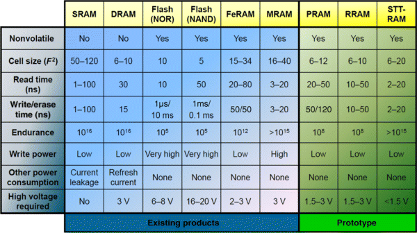
Table 4.1 summarizes characteristics of different memory technologies [1]. It compares current state of the art technologies including DRAM, SRAM, and Flash memories, as well as other prototype technologies including STT-RAM, FeRAM, and PCM. STT-RAM utilizes magnetic materials for data storage, is a nonvolatile memory, and unlike DRAM, does not require periodic refreshing of stored information. This also enables instant-on capabilities. The endurance of Flash memory is about 105 cycles and the writing time ranges from micro- to milli-seconds. STT-RAM is predicted to perform over 1015 write cycles and have writing times of less than 1 ns. Since transistors are not the main storage element of STT-RAM, its power dissipation during the “off state” of the device is much less than corresponding transistor-based memories. The fast writing speed combined with the extremely high endurance of STT-RAM meets the technical demands of CMOS-based memories. This makes STT-RAM a potential candidate for “universal memory” in future information technology.
Table 4.1 Characteristics of emerging memory technologies [3]
 |
4.2 Spin Transfer Torque
4.2.1 Background of Spin Transfer Torque
STT-RAM utilizes the magnetization direction of a ferromagnetic layer for data storage similar to magnetic media in Hard Disc Drives. As shown in Figure 4.1a, an STT-RAM cell stack consists of a ferromagnetic free layer (FL) and a reference layer (RL) separated by a nonmagnetic space layer (SL). The self-sustained ferromagnetic free layer (FL) can maintain the data in the event of power loss and results in data nonvolatility. The changes in the magnetization configuration of the FL and RL result in a difference in the resistance of the STT-RAM cell such that it is low (high) when the two layers are parallel (antiparallel).
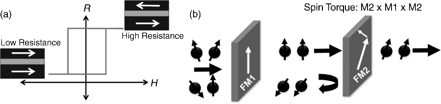
Figure 4.1 (a) Basic MRAM structure and magnetoresistive (MR) loop. (b) Spin torque transfer effect in a tri-layer magnetic structure (spacer layer is not shown)
In 1996, Slonczewski and Berger independently predicted that a nanomagnet could be directly switched by a current flowing through a tri-layer structure [4,5]. This switching behavior is known as the spin transfer torque effect. When electrons pass through a ferromagnetic (FM) layer, FM1, as shown in Figure 4.1b, the current becomes spin polarized due to the s-d interactions inside FM1. With the correct choice of the spacer layer material and thickness, the spin polarization is preserved during the traveling of the electrons from FM1 to FM2. At FM2, the polarized electrons exert a torque on the local magnetic moment due to a transfer of angular momentum. Given a sufficiently large injected spin polarized current, the spin torques can be large enough to change the magnetization of FM2.
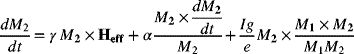
Slonczewski derived an expression to represent this torque and put it into the Landau–Lifshits–Gilbert equation [4,6]:
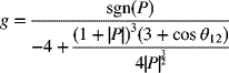
where g factor is defined as:
Mi is magnetic moment of the spin in the ith layer (i = 1,2), γ is gyromagnetic ratio (![]() ), Heff is the effective field that M2 feels, α is the Gilbert damping constant, I is the electrical current, e is the electron charge, P is the spin polarization ratio, and θ12 is the angle between M1 and M2. The first term of Equation 4.1 represents the precession of spin about the effective field direction. The last two terms represent the damping and the current induced spin torque terms, respectively.
), Heff is the effective field that M2 feels, α is the Gilbert damping constant, I is the electrical current, e is the electron charge, P is the spin polarization ratio, and θ12 is the angle between M1 and M2. The first term of Equation 4.1 represents the precession of spin about the effective field direction. The last two terms represent the damping and the current induced spin torque terms, respectively.
In 2000, Sun reported more details about the spin transfer torque mechanism [7]. He showed that there are three steps involved in the spin current induced magnetization switching: spin precession excitation, spin precession, and spin rotation. Figure 4.2a shows the model geometry for the calculation. The magnetic element has a geometric size of a × a × lm. M represents the magnetic moment and the current flow, I, with polarized spin S is along the –ex direction. With an effective field Heff, the M motion under applied spin current follows a spiral shape as shown in Figure 4.2b.
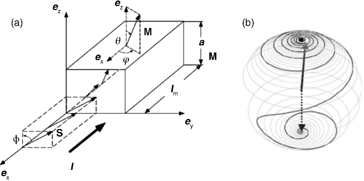
Figure 4.2 (a) Schematic showing various parameters used in the spin transfer torque critical switching current calculation. (b) Trajectory of the M under applied spin current. Switching of M is not instant, but rather it follows a spiral motion [7]
The spin torque from the spin current shifts the moment from its initial direction. Then, the moment starts to precess due to the precession torque of M × Heff as shown in Figure 4.2a. The angle between M and its initial magnetization direction becomes larger by increasing the input current density. With sufficient spin current, the precession angle of M becomes large enough to switch to the opposite direction. Sun also provided the critical switching current to induce the switching [7], given by:
Where η is the spin polarization ratio, α is the damping constant, Hk is the anisotropy field, and H is the applied field. Equation 4.3 provides guidance to reduce the critical switching current. For example, the switching current reduces upon increasing the magnetic spin polarization ratios or by having a magnetic layer with a smaller damping constant.
4.2.2 Experimental Observation of Spin Transfer Torque
Spin transfer torque provides an alternative way to drive a spintronic device. Magnetization can be switched directly by spin current instead of a magnetic field. There are extensive research studies on the current induced spin transfer torque for the switching of the magnetization. Spin transfer torque effect was first observed in magnetic nanowires [8,9]. When a current is injected along a magnetic nanowire, it is polarized within a nanometer range [10]. Spin current flows along the nanowire until it reaches a domain wall where the spin current exerts torques on the magnetic moments in the domain wall and forces the local magnetic moments to follow the direction of the spin current through exchange coupling. Therefore, for a constant input current, the domain wall is pushed along the current flow direction. It was demonstrated that the domain structure remains unaltered for the current density less than 107 A/cm2 where there is no breakdown in the domain wall structure [11]. Spin transfer torque effect was also observed in the point contact structure with Co/Cu multilayers and Co/Cu/Co sandwich structures [12,13] in which a sharp tip (D ∼ 100 nm) was used to contact a magnetic multilayer surface. The magnetic state of the multilayer is monitored by measuring the magnetoresistance of the contact. The point contact structure provides a relatively simple method to detect spin transfer torque effect. Since spin transfer occurs within, at most, a few magnetic domains beneath the tip and the domains are coupled to the continuous magnetic film, the dynamics of the spin transfer effects are affected. As a result, the current density required to observe spin transfer is an order of magnitude larger than in isolated magnetic structures, that is, nanopillar structures. There are other limitations with the structure: the point contact tip can damage the layers; the sample fabrication (i.e., contact formation) is not fully reproducible; the sample size can only be deduced from the resistance of the device.
Due to difficulties in the fabrication process, the first successful spin transfer torque switching was observed in 2000 by Katine et al. [14], four years after the theoretical prediction. A giant magnetoresistive (GMR) stack was prepared by sputtering the structure Cu(120 nm)/Co(10 nm)/Cu(6 nm)/Co(2.5 nm)/Cu(15 nm)/Pt(3 nm)/Au(60 nm) onto an oxidized Si substrate. A current perpendicular to plane (CPP) nanopillar structure with 100 nm diameter was fabricated and a schematic drawing of the device is shown in Figure 4.3a. The difference in thickness for the Co layers allows the magnetization direction of the thicker layer to be held fixed so that the polarity of the current bias associated with the spin transfer excitations in the thinner layer can be determined. Figure 4.3b shows the resistivity curve of the nanopillar with the applied current swept from negative to positive values. The high (low) resistance corresponds to the antiparallel (parallel) configuration between the thin and thick Co layers.
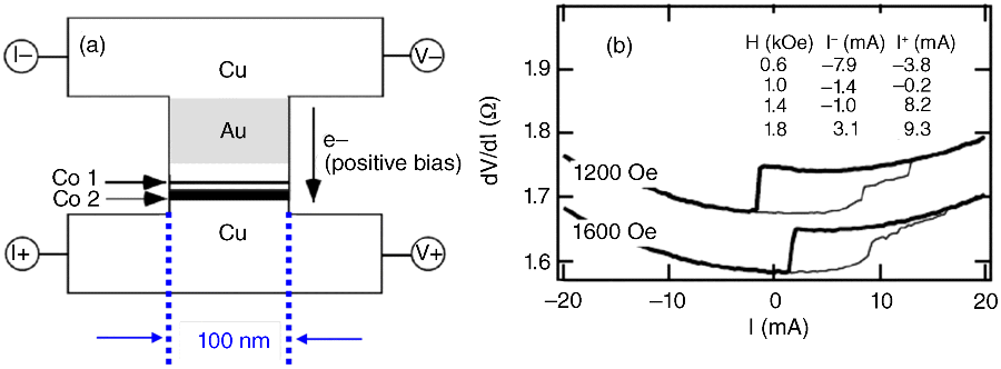
Figure 4.3 (a) Schematic drawing of a CPP GMR structure for spin transfer torque demonstration. (b) Current induced magnetization switching in CPP GMR devices [14]
4.3 STT-RAM Operation
4.3.1 Design of STT-RAM Cells
Magnetic RAM, or MRAM, is operated by magnetic fields which are generated from write line 1 which lies along the easy axis and a bit line (write line 2) which lies along the hard axis of the magnetic elements (Figure 4.4a and b). The MRAM element selected to be written lies at the intersection of a word line and bit line. The total magnetic field generated from the two lines is strong enough to switch the magnetization of the MRAM element, while the field produced from a single line seen by other elements is not large enough to induce switching. A single word or bit line cannot produce a field sufficient to induce switching, while their sum at their intersection is larger than the switching threshold required for writing.
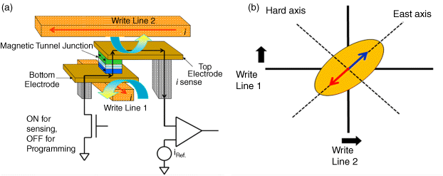
Figure 4.4 (a) Schematic drawing of MRAM. (b) Field generated by write lines 1 and 2 along the easy and hard axis
However, this writing process makes it difficult to efficiently scale MRAM. The magnetic orientation for MRAM elements relies on the shape anisotropy, which is sensitive to geometrical parameters of the cell. Small geometry variation or defects, which are unavoidable in fabrication, could induce large switching field distributions. Other memory cells along the bit line or word line may be switched when writing a specific cell. As a result, the operation window for such MRAM designs is narrow and is known as the half-field selection problem. The switching field distribution worsens with MRAM cell size shrinking. Therefore, it is difficult to achieve high density MRAM in this writing scheme.
Spin transfer torque provides a promising scheme to solve the half-field selection problem in field driven MRAM. Figure 4.5 shows a STT-RAM design operated by spin transfer torque where no magnetic field is required. The writing current directly goes through the memory element under the word line (transistor) control. Such design reduces the unintended writing errors. In addition, the writing current has better scalability since it is proportional to the device area according to Equation 4.3. STT-RAM has attracted attention due to its advantages, including scalability, speed, and power consumption [15,16].
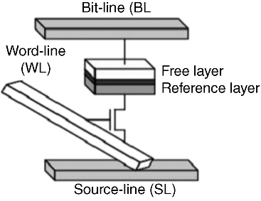
Figure 4.5 Spin transfer torque MRAM design [17]
A typical STT-RAM cell consists of one transistor to supply the current for writing and reading and one MTJ element for the actual storage of data (Figure 4.5). The generated voltage, which is proportional to Isense × Rlow × TMR, where Isense, Rlow, and TMR are the sense currents, low (parallel) resistance states, and TMR value, is then compared to a reference MTJ element to determine the state of the memory bit. In STT-RAM design, to achieve high memory density, the memory cell size can be as small as 4F2 based on the one MTJ and one transistor design scheme [17], where the width of transistor and MTJ is 1F.
It imposes great challenges in STT-RAM design as the lowest Jc (![]() ) required for writing STT-RAM (above 106 A/cm2) exceeds what a transistor can supply at 1F width. Although drive current of a transistor is proportional to its channel width, a larger transistor is not an option due to its negative impact to the STT-RAM capacity. Thus the current density required to switch the magnetization of the FL has to be reduced. With a low Jc, the voltage across the tunneling barrier is also low, thus improving the endurance and stability of STT-RAM.
) required for writing STT-RAM (above 106 A/cm2) exceeds what a transistor can supply at 1F width. Although drive current of a transistor is proportional to its channel width, a larger transistor is not an option due to its negative impact to the STT-RAM capacity. Thus the current density required to switch the magnetization of the FL has to be reduced. With a low Jc, the voltage across the tunneling barrier is also low, thus improving the endurance and stability of STT-RAM.
4.3.2 Key Parameters for Operation
STT-RAM utilizes MTJ structures instead of metallic giant magnetoresistive (GMR) structures. Metallic GMR devices have resistances of several ohms and small GMR ratios (<20%) [18–21]. As such, it is not a suitable structure to integrate with CMOS transistors and provide a sufficient signal to noise ratio. The MTJ structure is optimized to gain a high TMR signal as well as low product of resistance and area (RA). This is important for the MTJ to sustain a large switching current threshold and gain high data transfer rates. In 2004, the spin transfer torque effect was successfully demonstrated in a low RA MTJ structure based on an Al2O3 tunnel barrier [22–24]. Due to the electron incoherent tunneling mechanism in Al2O3, the maximum TMR value is only 70% in Al2O3 MTJ structures. In late 2004, a breakthrough of TMR around 200% was made by adopting a crystallized (001) MgO barrier layer with single crystal Fe (001) electrodes [25] or polycrystalline CoFe (001) electrodes [26]. Theoretical calculations show that the crystallized MgO barrier functions as a spin filter in a MTJ system. Only Δ1 states can coherently tunnel through the barrier, resulting in high spin polarization and high MR ratios. More recently, TMR values of around 600% and above have been achieved in CoFeB/MgO/CoFeB pseudo spin valve MTJs at room temperature [27–29]. Since then, MgO-based low RA MTJs with TMR above 150% and RA below 50 Ωμm2 [30,31] have become the most suitable structure to be used in STT-RAM.
Another consideration for STT-RAM is the size and scalability of the devices required for achieving high density STT-RAM. While sub-20 nm MTJ structures have been demonstrated [16,32], other factors such as transistor size, sense current, and thermal stability can still have an impact on the scalability of STT-RAM.
It was mentioned that STT-RAM has better scalability compared to field driven MRAM. Given a fixed Jc value, writing current amplitude keeps reducing with memory cell shrinking until it reaches the superparamagnetic limit [33,34] where the thermal energy, kBT, is equal to the energy barrier and the magnetization state is no longer stable. As the memory cell size is reduced to the nanometer scale, the amplitude of the energy barrier, ΔE, between the two stable states is reduced since ΔE is defined by [34,35]
where V is the volume and the anisotropy energy is defined as
The magnetization status change corresponds to forcing the memory elements to overcome the energy barrier E. Additionally, when T ≠ 0, thermal fluctuation can unintentionally increase the probability of the FL switching and result in data loss. Data storage typically demands the thermally activated hopping from one state to the other to be improbable over a period of 10 years or longer. Such hopping is known as thermally activated magnetic relaxation [36–38]. The data retention period is defined by
where τ0 is the attempt frequency (typically one nanosecond). ΔE, given by Equation 4.4, has to be large enough to overcome the magnetization degradation caused by thermal fluctuation to achieve the desired data retention period. With thermal fluctuations, the magnetization of the FL is gradually changed with time as
where t is the time and M0 is the initial magnetization when t = 0. Equation 4.7 indicates that M decays with time and the rate of decay depends on τ and therefore ΔE. However, if the memory cell size is so small that the thermal energy, kBT, is comparable to ΔE, τ is small and M decays very fast. To overcome this and achieve ultrahigh areal density, STT-RAM with very small volume requires a large Ku to maintain thermal stability.
As shown in Figure 4.6a, for a cell size of 30 nm, the minimum required Ku is about 7 × 10⁵ erg/cm3 to maintain a thermal stability factor above 60. The required Ku has to be further increased as the memory elements are scaled down. This imposes tremendous writing difficulty for STT-RAM. According to Equation 4.3, the critical switching current density depends on the demagnetization field (![]() ) and anisotropy field. For a large memory cell size, Jc is dominated by Hd since Hk (Ku) is negligible compared to Hd. However, for high areal density STT-RAM, Hk (Ku) has to be greatly increased for thermal stability and results in a large Jc as shown in Figure 4.6b.
) and anisotropy field. For a large memory cell size, Jc is dominated by Hd since Hk (Ku) is negligible compared to Hd. However, for high areal density STT-RAM, Hk (Ku) has to be greatly increased for thermal stability and results in a large Jc as shown in Figure 4.6b.
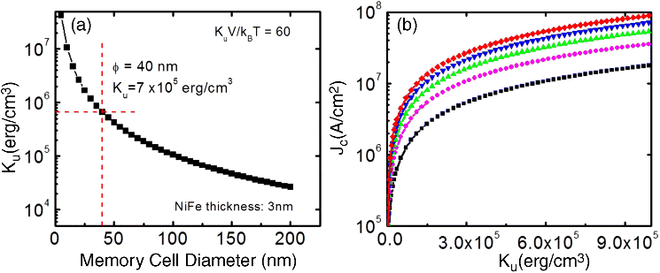
Figure 4.6 (a) Required Ku value to maintain thermal stability for high density STT-RAM. (b) Relationship between critical switching current density (Jc) and anisotropy energy (Ku). Different colors represent different values of damping constants
Another aspect affecting the scalability of STT-RAM is the sensing capabilities. As Jc decreases, the read current also needs to decrease in order to prevent accidental switching of the element since the switching probability depends on Jc as [39]
where τp, τ0, E, Ic and Ic0 are the current pulse width, attempt frequency, energy barrier, applied current, and critical switching current, respectively. In order to reduce the probability of switching, the read current needs to be reduced as the critical current for switching is reduced. Furthermore, as the MTJ devices are scaled down, variations in the device due to the fabrication process can result in reduction of the sensing current margin and affect the reliability of the device. As Isense decreases, the sense margin also decreases together with device variations at small scales, and it can lead to a large bit error rate in sensing and determination of the state of the memory cell [40,41].
4.4 STT-RAM with Perpendicular Anisotropy
In the previous sections, we have discussed STT-RAM with in-plane anisotropy where magnetizations of both FL and RL are in the film plane. However, there are major drawbacks when applying in-plane anisotropy for STT-RAM. In high density STT-RAM, large shape anisotropy (high aspect ratio) is required to maintain thermal stability and eventually limits the density. In addition, high aspect ratios are not preferred for fabrication processes, since geometry variations can change magnetic characteristics and result in nonuniformity of Jc. Furthermore, the existence of the demagnetization field (Hd = 4πMs), which does not contribute to the thermal stability, imposes difficulty on reduction of Jc for STT-RAM with in-plane anisotropy.
In 2006, Wang's group proposed and demonstrated spin transfer torque in a CPP GMR device with perpendicular anisotropy [42]. Jc in a perpendicular anisotropic system is given by
where Ku is perpendicular anisotropy, which could be interface anisotropy or crystalline anisotropy, and other parameters are similar to equation Equation 4.3. Equation 4.9 suggests that Jc depends on the effective perpendicular anisotropy ![]() , which can be adjusted by tuning layer structure and materials. As a consequence, Jc can be further reduced. Since perpendicular anisotropy is not a function of the shape anisotropy, memory cells can be circular in shape, which is favorable in reducing Jc distribution. Thus, STT-RAM with perpendicular anisotropy has better scalability and is acknowledged as the major direction in STT-RAM development [16,43,44].
, which can be adjusted by tuning layer structure and materials. As a consequence, Jc can be further reduced. Since perpendicular anisotropy is not a function of the shape anisotropy, memory cells can be circular in shape, which is favorable in reducing Jc distribution. Thus, STT-RAM with perpendicular anisotropy has better scalability and is acknowledged as the major direction in STT-RAM development [16,43,44].
In order to generate perpendicular magnetic anisotropy, a multilayer superlattice structure of [magnetic layer/nonmagnetic layer]n is very common where the nonmagnetic layer is usually a heavy metal such as Pt or Pd [45,46]. The total magnetic anisotropy energy (keff) of the multilayer system is defined [47]
where tm is the magnetic layer thickness, kcry is the crystalline anisotropy energy of the magnetic layer, ![]() is from the demagnetization field (Hd), and ks is the perpendicular anisotropy induced by interface effects. Positive keff value corresponds to a perpendicular magnetic anisotropy. Figure 4.7 shows an example of the magnetic layer thickness dependence of Keff × tm, in which the magnetic layer is Co and the nonmagnetic layer is Pd [47]. The product of Keff and tm linearly depends on tm, with a slope of (
is from the demagnetization field (Hd), and ks is the perpendicular anisotropy induced by interface effects. Positive keff value corresponds to a perpendicular magnetic anisotropy. Figure 4.7 shows an example of the magnetic layer thickness dependence of Keff × tm, in which the magnetic layer is Co and the nonmagnetic layer is Pd [47]. The product of Keff and tm linearly depends on tm, with a slope of (![]() ) and an intercept of 2ks. Magnetic anisotropy of the multilayer system is changed from perpendicular to in-plane with increasing magnetic layer thickness. Therefore, the anisotropy field (Hk) direction and amplitude of the multilayer system could be controlled by tuning the individual layer thicknesses [48,49].
) and an intercept of 2ks. Magnetic anisotropy of the multilayer system is changed from perpendicular to in-plane with increasing magnetic layer thickness. Therefore, the anisotropy field (Hk) direction and amplitude of the multilayer system could be controlled by tuning the individual layer thicknesses [48,49].
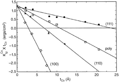
Figure 4.7 Magnetic layer thickness dependence of Keff × tm [47]
Figure 4.8a shows a M-H loop of a sheet film with perpendicular anisotropy. The square loop shape indicates that the easy axis of the FL and RL are out of plane. The two-step switching indicates that the magnetizations of the FL and RL are well separated. Spin transfer torque induced magnetization switching in the nanopillar measured at room temperature is shown in Figure 4.8b. The positive current is defined along the direction from the bottom to top electrode. Two sharp resistance changes indicate current induced magnetization switching of the FL where the two different resistance states represent when the FL and RL are aligned parallel or antiparallel. Since magnetization of the FL is parallel with the direction of current flow, Figure 4.8b provides strong experimental proof that spin transfer torque is the main switching mechanism instead of the Oersted field.
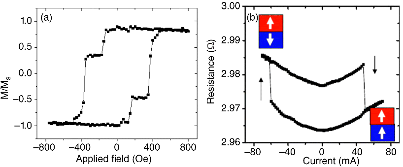
Figure 4.8 (a) M-H loop of a sheet film of GMR having perpendicular anisotropy. (b) Spin transfer torque in a spin valve with perpendicular anisotropy at room temperature [42]
Due to large Jc values (up to 108 A/cm2) and low GMR ratios, spin transfer torque on all metallic CPP GMR devices with perpendicular anisotropy is still not practical for STT-RAM. In 2007, Toshiba demonstrated spin transfer switching in a MTJ device with perpendicular anisotropy. Using MgO as the barrier and TbCoFe/CoFeB as the RL and FL, Jc was reduced to 3.6 × 10⁶ A/cm2 with TMR around 12% [50]. In 2008, Jc was further reduced to 2.7 × 10⁶ A/cm2 and TMR was increased to 60% in a MTJ with MgO as the barrier. The structure used [Co/Pd]/CoFeB and FePt/CoFeB as the FL and RL, respectively [51]. However, such Pd- or Pt-based multilayer structures or alloys have a large damping constant and leads to large Jc, as shown in Equation 4.9, and low TMR due to strong spin–orbit interactions. Most recently, Ikeda et al. demonstrated perpendicular anisotropy in a CoFeB/MgO system, which has been widely used to generate high TMR in MTJs with in-plane anisotropy [28]. A thin but continuous CoFeB film is adopted as the FL and RL to generate perpendicular anisotropy at the interfaces with the MgO barrier layer. The anisotropy with respect to CoFeB thickness is shown in Figure 4.9 [52]. Ikeda et al. showed with a proper annealing process, TMR of the system is more than 120% with RA around 18 Ω/μm2. The average intrinsic critical current density is 3.9 × 10⁶ A/cm2, which is close to the value for in-plane configuration. Successfully building perpendicular anisotropy on CoFeB/MgO systems provides a solid base for high areal density STT-RAM with high thermal stability, low critical switching current and high TMR values. However, material and structure engineering [53] is still necessary to further reduce Jc to less than 106 A/cm2, the requirement to be integrated with transistors for high density STT-RAM.
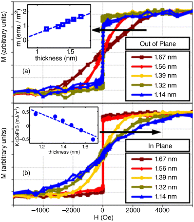
Figure 4.9 Dependence of the magnetic anisotropy on the thickness of CoFeB free layer [95]
4.5 Stack and Material Engineering for Jc Reduction
4.5.1 Dual Pinned Structure
Low critical switching current density and high thermal stability are two main foci in STT-RAM research and development. Theoretically, Jc can be further reduced by increasing the spin polarization ratio, reducing the damping constant, and reducing the saturation magnetization of the FL. However, these attempts offer little room for improvement due to material limitations and high TMR requirement. The research on stack layer engineering, such as dual pinned RL structures [54], provides another approach for Jc reduction. Figure 4.10 illustrates a stack structure with dual pinned reference layers. Two antiferromagnetic (AFM) pinning layers are adopted to bias the two RLs along opposite directions. The commonly used AFM materials are IrMn and PtMn in MTJ structures. The biasing direction can be set during the thermal annealing with application of a magnetic field. The FL is separated from the two RLs by two SLs which can be a metal or a tunneling barrier layer. Since the MR signal from the bottom and top parts are opposite to each other, the two SLs cannot be identical in order to gain an output signal.

Figure 4.10 Schematics of MTJ with dual pinned reference layers [57]
With the dual pinned RL structure, the efficiency of the spin scattering is greatly enhanced and the switching current density threshold is reduced as a result. With a high resistance value at the initial state, the magnetizations of the FL and bottom (top) RL are anti-parallel (parallel). As shown in the left diagram in Figure 4.10, polarized spin current will interact with the FL magnetization and align it with the magnetization of the bottom RL. The majority spins from the bottom RL will be reflected back by the top RL due to its opposite magnetization. Thus spin dynamic accumulation occurs between the two RLs [55,56]. When such spin accumulation exceeds a critical value, FL switching occurs. To switch the FL back, current polarity should be changed. Due to the symmetrical stack structure, spin can also be accumulated between the two FLs for both current polarities. With the spin accumulation, FL switching deviates from Equation 4.9 and a lower Jc is expected. Wang's group has successfully demonstrated that Jc amplitude can be reduced by factor of four with a dual pinned RL structure (in DC condition) [57]. Diao et al. further confirmed that such structure significantly reduces intrinsic Jc when excluding temperature effects [54].
Besides reduction of Jc amplitude, the dual pinned RL structure also improves the symmetry of Jc. For a MTJ with a single RL, switching of the FL is induced by either the majority spin (from high resistance to low resistance) or minority spin (from low resistance to high resistance). High spin polarization of the RL and FL is essential to ensure high TMR and reduce Jc. The two switching processes require different Jc amplitudes, resulting in asymmetrical writing current. In the dual pinned RL structure, it is the majority spins that induces switching regardless of the current polarity. Therefore, symmetry of Jc is improved with the two identical RLs.
One disadvantage of the dual pinned RL structure is the high stack resistance due to more layers introduced in the design. High voltage has to be applied to supply a large enough switching current density. Another drawback is relatively low TMR values. The total TMR signal is the sum of the TMR/GMR effects from the bottom and top parts. As magnetizations of the two RLs are opposite, magnetization of the FL is always parallel to one RL and antiparallel to the other RL so the measured resistance difference (ΔR) shrinks and results in a lower TMR signal.
4.5.2 Nanocurrent Channel Structure Design
Since a large transistor is required to supply enough current to write STT-RAM cells, the footprint of the memory cell can be quite big and can limit the density of a STT-RAM chip. For a given current amplitude, however, local current density can be increased if the current crossing area is reduced. A nanocurrent channel (NCC) integrated with a MTJ has been proposed by Wang et al. with Jc reduced by factor of three [58].
Figure 4.11a shows the MTJ stack with two FLs and one FL integrated with a NCC structure. A NCC can be built by lithographic patterning which is quite complicated and costly. One alternative approach is to build a NCC using direct co-sputtering. It is a feasible and cost-effective mechanism to build small NCC for STT-RAM of an effective size of 20 nm or less. Wang et al. has reported co-sputtering Fe and Si with oxygen doping to form granular FeSiO NCC with a diameter of about 5 nm [46,59,60] (Figure 4.11b). One highlight of co-sputtering is to form NCC or columnar (island) growth of Fe or FeSi, surrounded by SiO2 insulating boundaries. Since Si-O has relatively higher bonding energy, Fe atoms will survive from the oxygen atmosphere and form a column structure surrounded by SiO2 boundaries.
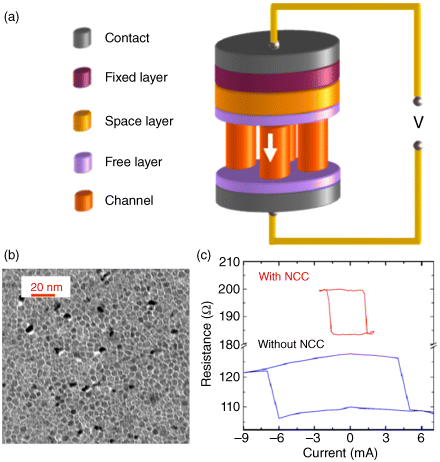
Figure 4.11 (a) MTJ stack integrated with nanocurrent channel structure. (b) Tunneling electron microscopy image of granular FeSiO nano current channel with diameter of about 5 nm [60]. (c) Switching characteristic of NCC device together with the device without NCC [58]
The FeSiO layer consists of magnetic conductive nanovolumes (Fe, Fe-Si) and insulating boundaries (SiO2). It can function as a current filter. If a current flows through the layer, it will be confined inside the conductive columns. Due to the reduced current cross-area (total area minus boundary area), the current density inside the nanocolumns will be increased. By adjusting the area ratio between the conductive areas and the boundary areas, the current density inside the conductive nanovolumes can be greatly increased. It provides a new approach to adjust the current distribution inside nanodevices that are sensitive to the current density.
Assuming the magnetizations of the FLs and RL are antiparallel at the beginning, electrons are polarized by the RL layer when they travel from the top layer to the bottom layer. Due to the current confining effect, the local current density in the current channels is increased. The magnetic moments (inside the magnetic NCC and FL 2) are reversed first and then spread the switching all over the free layer together with the help of the Fe or FeSi in FeSiO layer. After FL 2 switches, FL 1 is much easier to be switched because of the exchange coupling with FL 2 through the magnetic NCC. The reversed moments in the NCC, together with the polarized current, will switch the moment and results in switching of FL 1. In the switching process, the NCC layer is: (1) increasing the current density locally inside the nanochannels and the FL and (2) coupling with the two sub-free layers. Furthermore, since the FeSiO is “soft” due to its nanometer scale volume, its magnetic moment is much easier to be reversed (even under small polarized current). The reversed moment will help to switch FL 2. Under DC conditions, the spin transfer torque behavior of a MTJ with NCC is similar to that of a normal MTJ as shown in Figure 4.11c. As designed, the Jc of the former is significantly reduced from 1.4 × 10⁷ to 4.2 × 10⁶ A/cm2 and the symmetry of Jc for the two current polarities is also improved.
The switching process discussed above was induced under scanning of quasi-static DC current, in which thermally activated spin transfer occurred. Thermal fluctuation from the outside environment helps the spin current to switch the free layer. In reality, STT-RAM is driven by nanosecond current pulses; thermal assistant energy is excluded in such short time frame. Therefore, the critical switching current density is higher. The relationship between critical switching current density, Jc, and pulse width, τp, is [61]
where Jc0 is the intrinsic critical switching current density without thermal activated assistance. Equation 4.11 indicates that Jc is always smaller than Jc0 and equals Jc0 only at T = 0 K. Experimental results show that Jc0 is normally two or three times higher than the thermally assisted critical switching current, Jc, at room temperature. Equation 4.11 also can be used to evaluate the intrinsic switching current density and the thermal stability factor [39,62–64]. Wang's group reported that Jc0 is reduced from 2.4 × 10⁷ A/cm2 to 8.5 × 10⁶ A/cm2 with a NCC structure in MTJ.
4.5.3 Electric Field Assisted Switching
The previously mentioned methods for reducing Jc for MTJs involve changing the materials and stack structure or device design, but the magnetic properties of the material stay the same. Although there are studies that have been done using multiferroic materials [65,66], they are not commonly used in spintronic devices. It has recently been shown that the magnetic properties of ferromagnetic materials, particularly the perpendicular anisotropy, can be modified by the application of an electric field [67–69]. By tuning the magnetic properties, the energy barrier for magnetization switching can be reduced, resulting in a lower Jc for STT switching.
An electric field, which is generated by applying a voltage across a dielectric (in this case, MgO), can modify the electric properties of certain magnetic thin films by changing the electron density at the Fermi energy level. However, this effect is seen only near the interfaces between the FM and MgO and changes the interfacial anisotropy. As the ferromagnetic films become thicker, the demagnetization field and bulk crystalline anisotropy dominates over the interfacial anisotropy changes and diminishes the electric field modified anisotropy. Therefore, very thin films are required for electric field modification of the magnetic anisotropy. The perpendicular anisotropy energy density is given by [70,71]
where μ0, Ms, Ku, d, Ks1, Ks2, and ΔKs(V) are the permeability of free space, saturation magnetization, crystalline anisotropy, thickness of the ferromagnetic film, surface anisotropy from the first interface, surface anisotropy from the second interface, and induced surface anisotropy due to an applied voltage, respectively.
The first experimental evidence showing that electric fields could be used to modify magnetic anisotropy was show in 2007 [72]. FePt and FePd thin films were epitaxially grown on MgO(001) and by the application of −0.6 V, a 4.5% and 1% change in the coercivity were observed for the FePt and FePd films, respectively.
In 2009, electric field induced magnetic anisotropy changes were demonstrated for BCC Fe(001)/MgO(001) junctions where the Fe thin film was a few monolayers thick [73] as well as for several monolayers of FeCo/MgO [74]. Using optical Kerr measurements, it was demonstrated that the anisotropy could be modified by about 40%, changing from −31.3 to −13.7 kJ/m3 with the application of 200 and −200 V [73]. By changing the applied voltage, and therefore strength of electric field at the interface between the ferromagnetic material and MgO, the magnetization of the FeCo films can be changed from in-plane to perpendicular, as shown in Figure 4.12 [74].

Figure 4.12 (a, b) Change in the magnetic anisotropy from in-plane to perpendicular due to the applied electric field in FeCo films [73]
The application of an electric field for magnetic anisotropy modification has not only been shown in thin films, but also in MTJs. In 2011, electric field assisted switching in a CoFeB/MgO/CoFeB MTJ was demonstrated [70]. An appropriate bias field is applied for operation of the device and then through application of an electric field, the coercivity change results in changing the FL and RL magnetization between parallel and antiparallel. The coercivity of the FL (RL) changes from 72 Oe (115 Oe) to 20 Oe (137 Oe) with the application of a bias voltage of Vbias = −870 mV (+890 mV). Additionally, by applying bias voltages of −0.9 V and −1.5 V, the critical switching current density required for STT switching of the devices was reduced to −1.2 × 10⁴ and −2.4 × 10⁴ A/cm2. If this electric field control of the magnetic anisotropy is integrated with STT-RAM devices, it will significantly reduce the writing current and improve the energy efficiency of the devices.
4.6 Ultra-Fast Switching of MTJs
An important issue to consider with STT-RAM is the write speed. Spin torque switching on the picosecond scale has been demonstrated for MTJs [75,76]. In order to achieve this ultra-fast switching, an orthogonal MTJ structure has been adopted, which consists of an in-plane FL and two polarizing layers, one in-plane and one orthogonal to the plane. The structure used in [77] has the following structure: bottom lead/in-plane polarizer/barrier layer/free layer/barrier/perpendicular polarizer/capping layer. The magnetoresistance value is due to the orientation of the free layer relative to the in-plane polarizing layer. In a traditional in-plane MTJ, the initial torque exerted on the free layer is small since it depends on the angle between the different magnetic layers as seen by Equation 4.1. However, the addition of an orthogonal polarizing layer results in a large initial spin torque. The magnetization trajectories for the case of a traditional in-plane MTJ and orthogonal MTJ are shown in Figure 4.13a and b. The trajectories were calculated using a macro spin approximation of the Landau–Lifshitz–Gilbert equation with the STT term. From the magnetization trajectories, we can see that the free layer magnetization of the orthogonal MTJ is quickly switched to out-of-plane and results in a faster switching speed. “To demonstrate the switching of the orthogonal MTJ, voltage pulses of varying widths and magnitudes were used and the requirements for 50% switching probability was determined. At an excitation voltage of 1.58 V, the switching time could be reduced to 120 ps without the aid of an external bias field.
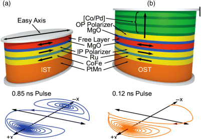
Figure 4.13 (a) Magnetization trajectories for an in-plane MTJ (b) for orthogonal MTJ [77]
In 2012, Zhao et al. [78] utilized a CoFeB/MgO/CoFeB MTJ structure with Fe rich CoFeB. The Fe rich CoFeB results in a strong perpendicular interface anisotropy, but the magnetization of the magnetic layers remains in-plane. They demonstrated that for a 50% switching probability, a 165 ps pulse width was required, and for a switching probability of 98%, the required pulse width was 190 ps where the excitation pulse amplitude was 1.89 V. This corresponds to switching energies of 0.16 and 0.21 pJ for 50 and 98% switching probabilities, respectively. The fast switching of the devices is attributed to a reduction in the out-of-plane demagnetization field due to the perpendicular interface anisotropy.
4.7 Spin–Orbit Torques for Memory Application
Recently, the study of current induced spin–orbit torques in ultrathin magnetic structures in the absence of a spin polarizer has attracted a strong interest among researchers due to its potential for low power magnetization switching [79–83]. Different phenomena, such as the Rashba effect [79,80] and the spin Hall effect [14,84], have been proposed to explain the current induced torques with an in-plane current. In this section, we briefly discuss the Rashba and spin Hall effects and present some of the recent progress in this area.
Although the Rashba effect was known in semiconductor materials for a long time [85], it recently has been found that the current induced Rashba field could be comparable to current induced spin transfer torque in metallic systems [79,86]. An ultra-thin film of magnetic layer (∼1 nm) is sandwiched between a nonmagnetic metal and insulating layer. The nonmagnetic metal layer must have strong spin–orbit coupling such as Ta, Pt, and Pd. Due to the inversion asymmetry of multilayer thin films, the conduction electrons feel a net electric field caused by an asymmetric Coulomb potential profile. Furthermore, presence of strong spin–orbit coupling in the transition ferromagnetic metallic system interprets this electric field to an equivalent magnetic field. The magnitude of the Rashba field, Hra, is given by [87,88]:
where μB is the Bohr magneton, Ms is the saturation magnetization, P is a parameter that represents the s-d electron coupling strength, αR is the Rashba coefficient (proportional to the spin–orbit strength of the material) and Je is the input current density. Although the Rashba field is concentrated only at the interface of the magnetic and nonmagnetic layers, its intensity could be quite large (the order of 1 Tesla for a current density of about 108 A/cm2) [79,80,87].
In 2012, another proposal came out that suggested spin–orbit torque originated from the spin Hall effect [14]. In a material with a strong spin–orbit coupling, electrons with opposite spins deflect in different directions according to ![]() where E is the applied electric field, σ is the electron spin direction, and Js is the generated spin current. The direction of the accumulated spin at the boundary of the nonmagnetic layer is shown in Figure 4.14a. Since spin accumulates at each boundary of the material, the presence of a magnetic material at the interface with the nonmagnetic channel results in the absorption of the spin current and application of spin torque on the magnetic moments.
where E is the applied electric field, σ is the electron spin direction, and Js is the generated spin current. The direction of the accumulated spin at the boundary of the nonmagnetic layer is shown in Figure 4.14a. Since spin accumulates at each boundary of the material, the presence of a magnetic material at the interface with the nonmagnetic channel results in the absorption of the spin current and application of spin torque on the magnetic moments.
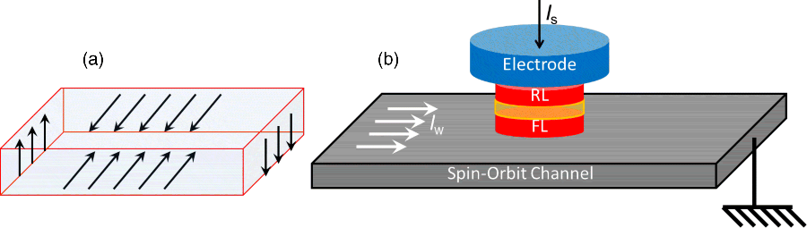
Figure 4.14 (a) Splitting of the electron spins due to the spin orbit effect. (b) Schematic of a three terminal device that operates based on the spin orbit torque
Recently, there have been some reports on the characterization of both torques in the magnetic multilayer structures [89,90]. In spite of fact that which effect is the dominant mechanism of the magnetization switching, spin orbit torque is a promising candidate for the magnetization switching. There has been a proposal of a three terminal device shown in Figure 4.14b that utilizes the spin orbit torques for the magnetization writing [14]. In this device, the writing and reading have different paths. For writing of the data on the magnetic layer, a current is passed through the spin orbit channel; for the reading, a small current is passed through the MTJ stack.
The three-terminal device has several advantages over the conventional STT-RAM memory cell. Since the read and write current paths are separated, each path can be optimized for its specific purpose. By preventing the passage of large current through the tunnel barrier, there is no breakdown issue. It has been shown that the efficiency of the spin Hall induced spin torque is higher than the conventional spin transfer torque effect [81]. Furthermore, the Joule heating can be significantly reduced since the write path can have much lower resistance. In addition, the MTJ can be optimized for a large TMR. Finally, other switching mechanism such as electric field assisted switching can be easily integrated with the three-terminal device.
4.8 Current Demonstrations for STT-RAM
The first demonstration of STT-RAM was in 2005 by Sony where they demonstrated the first 4 kbit STT-RAM [91]. Hitachi and Tohuku University announced their 2 Mbit STT-RAM in 2008 [92] and later demonstrated in 2009 a 32 Mbit STT-RAM. Grandis has announced their low power STT-RAM where the writing energy is 0.16 pJ with a write current of 80 μA, write voltage of 0.4 V and write speed of 5 ns [93]. Everspin announced in November 2012 the release of their 64 Mbit STT-RAM [94].
4.9 Summary and Perspectives
STT-RAM is a competitive memory technology which is nonvolatile, fast and endurable. It offers a simpler cell structure compared to MRAM and allows for better scalability. It can be a universal memory for personal electronic devices, automobile, and space technology. After years of development, STT-RAM chips have been commercialized for embedded memory applications. The crucial issue of STT-RAM is the high critical switching current density for writing process, which requires even higher current to achieve faster write speeds.
Various cell structures and material engineering methods have been proposed and shown to successfully reduce critical switching current density without degrading the thermal stability of the STT-RAM cell. Utilization of MgO as the tunnel barrier for MTJs has brought many advantages for STT-RAM. Successful integration of MgO MTJs with spin transfer torque brings critical switching current density down to 1 × 10⁶ A/cm2 and TMR values of more than 150%. However, utilizing shape anisotropy will eventually limit chip capacity for in plane STT-RAM. MTJs with perpendicular anisotropy, both due to interfacial anisotropy or crystalline anisotropy, have better scalability and higher spin transfer efficiency in terms of thermal stability over critical switching current density. Spin transfer torque together with perpendicular anisotropic MTJs is a promising candidate for high areal density STT-RAM. It has also been shown that electric field assisted switching can be used to reduce the writing energy. Furthermore, recent progresses on the spin-orbit torques demonstrate an exciting approach to solve most of the STT-RAM issues and introduce a new device structure for the STT-RAM memory cell.
References
- 1. The International Technology Roadmap for Semiconductors (ITRS) Emerging Research Devices (2011) ITRS Online. http://www.itrs.net/Links/2011ITRS/2011Chapters/2011ERD.pdf (accessed 16 January 2014).
- 2. Daughton, J.M. (1997) Magnetic tunneling applied to memory (invited). Journal of Applied Physiology, 81(8), 3758.
- 3. Future Fab (2014) www.future-fab.com/documents.asp?d_ID=4400 (accessed 16 January 2014).
- 4. Slonczewski, J. (1996) Current-driven excitation of magnetic multilayers. Journal of Magnetism and Magnetic Materials, 8853(96), 53–58.
- 5. Berger, L. (1996) Emission of spin waves by a magnetic multilayer traversed by a current. Physical Review B-Condensed Matter, 54 (13), 9353–9358.
- 6. Slonczewski, J.C. (1996) Current-driven excitation of magnetic multilayers. Journal of Magnetism and Magnetic Materials, 8853(96), 93–98.
- 7. Sun, J. (2000) Spin-current interaction with a monodomain magnetic body: A model study. Physical Review B-Condensed Matter, 62(1), 570–578.
- 8. Partin, D.L., Karnezos, M., deMenezes, L.C., and Berger, L. (1974) Nonuniform current distribution in the neighborhood of a ferromagnetic domain wall in cobalt at 4.2K. Journal of Applied Physiology, 45(4), 1852.
- 9. DeLuca, J.C. and Gambino, R.J. (1979) Abstract: Bias field dependence of domain drag propagated bubble domains. Journal of Applied Physiology, 50(B3), 2212.
- 10. Togawa, Y., Kimura, T., Harada, K. et al. (2006) Current-excited magnetization dynamics in narrow ferromagnetic wires. Japanese Journal of Applied Physics, 45(27), L683–L685.
- 11. Mougin, A., Cormier, M., Adam, J.P. et al. (2007) Domain wall mobility, stability and Walker breakdown in magnetic nanowires. Europhysics Letters, 78(5), 57007.
- 12. Tsoi, M., Jansen, A., Bass, J. et al. (1998) Excitation of a magnetic multilayer by an electric current. Physical Review Letters, 80(19), 4281–4284.
- 13. Ralls, K.S., Buhrman, R.a., and Tiberio, R.C. (1989) Fabrication of thin-film metal nanobridges. Applied Physics Letters, 55(23), 2459.
- 14. Katine, J., Albert, F., Buhrman, R. et al. (2000) Current-driven magnetization reversal and spin-wave excitations in Co/Cu/Co pillars. Physical Review Letters, 84(14), 3149–3152.
- 15. Hu, J.-M., Li, Z., Chen, L.-Q., and Nan, C.-W. (2011) High-density magnetoresistive random access memory operating at ultralow voltage at room temperature. Nature Communications, 2, 553.
- 16. Klostermann, U.K., Angerbauerl, M., Grtining, U. et al. (2007) A perpendicular spin torque switching based MRAM for the 28nm technology node. IEEE International Electron Devices Meeting, Technical Digest, 2007, 187–190.
- 17. Wang, X., Chen, Y., Li, H. et al. (2008) Spin torque random access memory down to 22nm technology. IEEE Transactions on Magnetics, 44(11), 2479–2482.
- 18. Chappert, C., Fert, A. and VanDau, F F.N. (2007) The emergence of spin electronics in data storage. Nature Materials, 6(11), 813–823.
- 19. Fert, A. and Piraux, L. (1999) Magnetic nanowires. Journal of Magnetism and Magnetic Materials, 200(1), 338–358.
- 20. Binasch, G., Grünberg, P., Saurenbach, F., and Zinn, W. (1989) Enhanced magnetoresistance in layered magnetic structures with antiferromagnetic interlayer exchange. Physical Review B-Condensed Matter, 39(7), 4828–4830.
- 21. Dieny, B., Humbert, P., Speriosu, V. et al. (1992) Giant magnetoresistance of magnetically soft sandwiches: Dependence on temperature and on layer thicknesses. Physical Review B-Condensed Matter, 45(2), 806–813.
- 22. Huai, Y., Albert, F., Nguyen, P. et al. (2004) Observation of spin-transfer switching in deep submicron-sized and low-resistance magnetic tunnel junctions. Applied Physics Letters, 84(16), 3118.
- 23. Fuchs, G.D., Emley, N.C., Krivorotov, I.N. et al. (2004) Spin-transfer effects in nanoscale magnetic tunnel junctions. Applied Physics Letters, 85(7), 1205.
- 24. Meng, H., Wang, J., Diao, Z., and Wang, J.-P. (2005) Low resistance spin-dependent magnetic tunnel junction with high breakdown voltage for current-induced-magnetization-switching devices. Journal of Applied Physiology, 97(10), 10C926.
- 25. Yuasa, S., Nagahama, T., Fukushima, A. et al. (2004) Giant room-temperature magnetoresistance in single-crystal Fe/MgO/Fe magnetic tunnel junctions. Nature Materials, 3(12), 868–871.
- 26. Parkin, S.S.P., Kaiser, C., Panchula, A. et al. (2004) Giant tunnelling magnetoresistance at room temperature with MgO (100) tunnel barriers. Nature Materials, 3(12), 862–867.
- 27. Ikeda, S., Hayakawa, J., Ashizawa, Y. et al. (2008) Tunnel magnetoresistance of 604% at 300K by suppression of Ta diffusion in CoFeB/MgO/CoFeB pseudo-spin-valves annealed at high temperature. Applied Physics Letters, 93(8), 82508.
- 28. Ikeda, S., Miura, K., Yamamoto, H. et al. (2010) A perpendicular-anisotropy CoFeB-MgO magnetic tunnel junction. Nature Materials, 9(9), 721–724.
- 29. Bai, Z., Shen, L., Wu, Q. et al. (2013) Boron diffusion induced symmetry reduction and scattering in CoFeB/MgO/CoFeB magnetic tunnel junctions. Physical Review B-Condensed Matter, 87(1), 014114.
- 30. Diao, Z., Pakala, M., Panchula, A. et al. (2006) Spin-transfer switching in MgO-based magnetic tunnel junctions (invited). Journal of Applied Physiology, 99(8), 08G510.
- 31. Han, X., Ali, S.S., and Liang, S. (2012) MgO(001) barrier based magnetic tunnel junctions and their device applications. Science China Physics, Mechanics & Astronomy, 56(1), 29–60.
- 32. Jeong, J.H., Kim, Y., Lim, W.C. et al. (2011) Extended scalability of perpendicular STT-MRAM towards sub-20nm MTJ node, in 2011 International Electron Devices Meeting, pp. 24.1.1–24.1.4.
- 33. Speliotis, D.E. (1999) Magnetic recording beyond the first 100 Years. Journal of Magnetism and Magnetic Materials, 193(1–3), 29–35.
- 34. White, R.M. (2001) Magnetic recording — Pushing back the superparamagnetic barrier. Journal of Magnetism and Magnetic Materials, 226–230, 2042–2045.
- 35. Chappert, C., Fert, A., and F. N., VanDau. (2007) The emergence of spin electronics in data storage. Nature Materials, 6(11), 813–823.
- 36. Neel, L. (1949) Théorie du traînage magnétique des ferromagnétiques en grains fins avec application aux terres cuites. Annales De Geophysique, 5, 99–136.
- 37. Brown, W.J. (1963) Thermal fluctuations of a single-domain particle. Physical Review, 34(1951), 1677–1686.
- 38. Cowburn, R.P. (2003) Superparamagnetism and the future of magnetic random access memory. Journal of Applied Physiology, 93(11), 9310.
- 39. Yagami, K., Tulapurkar, a.a., Fukushima, A., and Suzuki, Y. (2004) Low-current spin-transfer switching and its thermal durability in a low-saturation-magnetization nanomagnet. Applied Physics Letters, 85(23), 5634.
- 40. Chen, E., Apalkov, D., Driskill-Smith, A. et al. (2012) Progress and Prospects of Spin Transfer Torque Random Access Memory. IEEE Transactions on Magnetics, 48(11), 3025–3030.
- 41. Article, R. Challenges for semiconductor spintronics, vol. i, pp. 40–44.
- 42. Meng, H. and Wang, J.-P. (2006) Spin transfer in nanomagnetic devices with perpendicular anisotropy. Applied Physics Letters, 88(17), 172506.
- 43. Mangin, S., Ravelosona, D., Katine, J.a. et al. (2006) Current-induced magnetization reversal in nanopillars with perpendicular anisotropy. Nature Materials, 5(3), 210–215.
- 44. Zhu, X. and Zhu, J.-G. (2006) Spin Torque and field-driven perpendicular MRAM designs scalable to multi-gb/chip capacity. IEEE Transactions on Magnetics, 42(10), 2739–2741.
- 45. Iwasaki, S. (2012) Perpendicular magnetic recording—Its development and realization. Journal of Magnetism and Magnetic Materials, 324(3), 244–247.
- 46. Wang, J., Shen, W., and Bai, J. (2005) Perpendicular magnetic recording, vol. 41, no.10, 3181–3186.
- 47. Engel, B., England, C., Van Leewen, R.A. et al. (1991) Interface magnetic anisotropy in epitaxial superlattices. Physical Review Letters, 67(14), 1910–1913.
- 48. Ding, Y., Judy, J.H., and Wang, J.-P. (2005) Magneto-resistive read sensor with perpendicular magnetic anisotropy. IEEE Transactions on Magnetics, 41(2), 707–712.
- 49. Shi, J., Tehrani, S., and Scheinfein, M.R. (2000) Geometry dependence of magnetization vortices in patterned submicron NiFe elements. Applied Physics Letters, 76(18), 2588.
- 50. Nakayama, M., Kai, T., Shimomura, N. et al. (2008) Spin transfer switching in TbCoFe/CoFeB/MgO/CoFeB/TbCoFe magnetic tunnel junctions with perpendicular magnetic anisotropy. Journal of Applied Physiology, 103(7), 07A710.
- 51. Nagase, T., Nakayama, M., Shimomura, N. et al. (2008) Spin transfer torque switching in perpendicular magnetic tunnel junctions with Co based multilayer. 2008 APS March Meeting, 53(2), C1.00331.
- 52. Amiri, P. Khalili., Zeng, Z.M., Langer, J. et al. (2011) Switching current reduction using perpendicular anisotropy in CoFeB–MgO magnetic tunnel junctions. Applied Physics Letters, 98(11), 112507.
- 53. Zhu, X. and Zhu, J.-G. (2007) Effect of damping constant on magnetic switching in spin torque driven perpendicular MRAM. IEEE Transactions on Magnetics, 43(6), 2349–2351.
- 54. Diao, Z., Panchula, A., Ding, Y. et al. (2007) Spin transfer switching in dual MgO magnetic tunnel junctions. Applied Physics Letters, 90(13), 132508.
- 55. Jiang, Y., Abe, S., Ochiai, T. et al. (2004) Effective reduction of critical current for current-induced magnetization switching by a Ru layer insertion in an exchange-biased spin valve. Physical Review Letters, 92(16), 167204.
- 56. Parkin, S.S.P., Roche, K.P., Samant, M.G. et al. (1999) Exchange-biased magnetic tunnel junctions and application to nonvolatile magnetic random access memory (invited). Journal of Applied Physiology, 85(8), 5828.
- 57. Meng, H., Wang, J., and Wang, J.-P. (2006) Low critical current for spin transfer in magnetic tunnel junctions. Applied Physics Letters, 88(8), 82504.
- 58. Meng, H. and Wang, J.-P. (2006) Composite free layer for high density magnetic random access memory with lower spin transfer current. Applied Physics Letters, 89(15), 152509.
- 59. Wang, J.-P., Shen, W.K., Bai, J.M. et al. (2005) Composite media (dynamic tilted media) for magnetic recording. Applied Physics Letters, 86(14), 142504.
- 60. Shen, W.K., Bai, J.M., Victora, R.H. et al. (2005) Composite perpendicular magnetic recording media using [Co/PdSi][sub n] as a hard layer and FeSiO as a soft layer. Journal of Applied Physiology, 97(10), 10N513.
- 61. Koch, R., Katine, J., and Sun, J. (2004) Time-resolved reversal of spin-transfer switching in a nanomagnet. Physical Review Letters, 92(8), 88302.
- 62. Braganca, P.M., Krivorotov, I.N., Ozatay, O. et al. (2005) Reducing the critical current for short-pulse spin-transfer switching of nanomagnets. Applied Physics Letters, 87(11), 112507.
- 63. Huai, Y., Pakala, M., Diao, Z., and Ding, Y. (2005) Spin-transfer switching current distribution and reduction in magnetic tunneling junction-based structures. IEEE Transactions on Magnetics, 41(10), 2621–2626.
- 64. Yagami, K., Tulapurkar, a.a., Fukushima, A., and Suzuki, Y. (2005) Inspection of intrinsic critical currents for spin-transfer magnetization switching. IEEE Transactions on Magnetics, 41(10), 2615–2617.
- 65. Eerenstein, W., Wiora, M., Prieto, J.L. et al. (2007) Giant sharp and persistent converse magnetoelectric effects in multiferroic epitaxial heterostructures. Nature Materials, 6(5), 348–351.
- 66. Hur, N., Park, S., Sharma, P.A. et al. (2004) Electric polarization reversal and memory in a multiferroic material induced by magnetic fields. Nature, 429(6990), 392–395.
- 67. Lottermoser, T., Lonkai, T., Amann, U., and Fiebig, M. (2004) Magnetic phase control by an electric field, vol. 193, no. May, pp. 541–544.
- 68. Ohno, H., Chiba, D., Matsukura, F. et al. (2000) Electric-field control of ferromagnetism. Nature, 408(6815), 944–946.
- 69. Chu, Y.-H., Martin, L.W., Holcomb, M.B. et al. (2008) Electric-field control of local ferromagnetism using a magnetoelectric multiferroic. Nature Materials, 7(6), 478–482.
- 70. Wang, W.-G., Li, M., Hageman, S., and Chien, C.L. (2012) Electric-field-assisted switching in magnetic tunnel junctions. Nature Materials, 11(1), 64–68.
- 71. Kanai, S., Yamanouchi, M., Ikeda, S. et al. (2012) Electric field-induced magnetization reversal in a perpendicular-anisotropy CoFeB-MgO magnetic tunnel junction. Applied Physics Letters, 101(12), 122403.
- 72. Weisheit, M., Fähler, S., Marty, A. et al. (2007) Electric field-induced modification of magnetism in thin-film ferromagnets. Science, 315(5810), 349–351.
- 73. Maruyama, T., Shiota, Y., Nozaki, T. et al. (2009) Large voltage-induced magnetic anisotropy change in a few atomic layers of iron. Nature Nanotechnology, 4, 158–161.
- 74. Shiota, Y., Maruyama, T., Nozaki, T. et al. (2009) Voltage-assisted magnetization switching in ultrathin Fe 80 Co 20 alloy layers. Applied Physics Express, 2, 63001.
- 75. Sun, Z., Wu, W., Incorporated, Q., and Diego, S. (2012) A Dual-mode Architecture for Fast-Switching STT-RAM.
- 76. Kitagawa, E., Fujita, S., Nomura, K. et al. (2012) Impact of ultra low power and fast write operation of advanced perpendicular MTJ on power reduction for high-performance mobile CPU, 2012 Int. Electron Devices Meet., pp. 29.4.1–129.4.4.
- 77. Rowlands, G.E., Rahman, T., Katine, J.a. et al. (2011) Deep subnanosecond spin torque switching in magnetic tunnel junctions with combined in-plane and perpendicular polarizers. Applied Physics Letters, 98(10), 102509.
- 78. Zhao, H., Glass, B., Amiri, P.K. et al. (2012) Sub-200ps spin transfer torque switching in in-plane magnetic tunnel junctions with interface perpendicular anisotropy. Journal of Physics D-Applied Physics, 45(2), 25001.
- 79. Gambardella, P. and Miron, I.M. (2011) Current-induced spin-orbit torques. Philosophical Transactions. Series A, Mathematical, Physical, and Engineering Sciences Royal Society (Great Britain), 369(1948), 3175–3197.
- 80. Avci, C. Onur., Garello, K., Miron, I. Mihai. et al. (2012) Magnetization switching of an MgO/Co/Pt layer by in-plane current injection. Applied Physics Letters, 100(21), 212404.
- 81. Liu, L., Pai, C.-F., Li, Y. et al. (2012) Spin-torque switching with the giant spin hall effect of tantalum. Science, 336 (6081), 555–558.
- 82. Ha, S.-S., Yoon, J., Lee, S. et al. (2009) Spin wave quantization in continuous film with stripe domains. Journal of Applied Physiology, 105(7), 07D544.
- 83. Suzuki, T., Fukami, S., Ishiwata, N. et al. (2011) Current-induced effective field in perpendicularly magnetized Ta/CoFeB/MgO wire. Applied Physics Letters, 98(14), 142505.
- 84. Liu, L., Moriyama, T., Ralph, D.C., and Buhrman, R.A. (2011) Spin-torque ferromagnetic resonance induced by the spin hall effect. Physical Review Letters, 106(3), 36601.
- 85. Chernyshov, A., Overby, M., Liu, X. et al. (2009) Evidence for reversible control of magnetization in a ferromagnetic material by means of spin–orbit magnetic field. Nature Physics, 5(9), 656–659.
- 86. Miron, I.M., Gaudin, G., Auffret, S. et al. (2010) Current-driven spin torque induced by the Rashba effect in a ferromagnetic metal layer. Nature Materials, 9(3), 230–234.
- 87. Suzuki, T., Fukami, S., Ishiwata, N. et al. (2011) Current-induced effective field in perpendicularly magnetized Ta/CoFeB/MgO wire. Applied Physics Letters, 98(14), 142505.
- 88. Pi, U.H., Kim, K.Won., Bae, J.Y. et al. (2010) Tilting of the spin orientation induced by Rashba effect in ferromagnetic metal layer. Applied Physics Letters, 97(16), 162507.
- 89. Jamali, M., Narayanapillai, K., Qiu, X. et al. (2013) Spin-orbit torques in Co/Pd multilayer nanowires. Physical Review Letters, 111(24), 246602.
- 90. Kim, J., Sinha, J., Hayashi, M. et al. (2013) Layer thickness dependence of the current-induced effective field vector in Ta|CoFeB|MgO. Nature Materials, 12(3), 240–245.
- 91. Hosomi, M., Yamagishi, H., Yamamoto, T. et al. (2005.) Technical report. IEEE International Electron Devices Meeting, Technical Digest, 459, 19–20.
- 92. Kawahara, T., Takemura, R., Miura, K. et al. (2008) 2 Mb SPRAM (SPin-Transfer Torque RAM) with Bit-by-Bit Bi-directional current write and parallelizing-direction current read. IEEE Journal of Solid-State Circuits, 43(1), 109–120.
- 93. Grandis (2010) “Grandis Newsletter,” Gd. Newsl., vol. 3, no. Q2.
- 94. Everspin (2012) ST-MRAM Press Release.
- 95. Amiri, P. Khalili., Zeng, Z.M., Langer, J. et al. (2011) Switching current reduction using perpendicular anisotropy in CoFeB–MgO magnetic tunnel junctions. Applied Physics Letters, 98(11), 112507.