
26
Outlook for Nanoelectronic Devices
An Chen1, James Hutchby2, Victor V. Zhirnov2, and George Bourianoff3
1GLOBALFOUNDRIES Inc., USA
2Semiconductor Research Corporation, USA
3Components Research Group, Intel Corporation, USA
26.1 Introduction
The purpose of this chapter is to summarize the potential of emerging research devices to perform their intended memory or information processing function benchmarked against current memory or CMOS technologies. These targeted functions include: (1) to extend and/or eventually replace CMOS with a highly scalable, high performance, low power information processing device technology and (2) to provide a memory or storage technology capable of scaling either volatile or nonvolatile memory technology beyond the 15 nm generation.
Two independent methods have been used to assess emerging devices. In a so-called “quantitative logic benchmarking,” emerging logic devices are evaluated by their operations in conventional Boolean Logic circuits, for example, a unity gain inverter, a two-input NAND gate, and a 32-bit adder. Metrics evaluated include speed, areal footprint, power dissipation, and so on. Each parameter is compared with that of the projected high-performance and low-power 15 nm CMOS. In the second method, referred to as “survey-based benchmarking,” ITRS Emerging Research Device (ERD) group conducts a survey among international experts to evaluate each emerging device technology against eight criteria normalized to high-performance CMOS for logic or to the memory technology targeted for replacement. The rating for each criterion reflects consensus opinions on the potential and maturity of these technology entries.
An important issue regarding emerging charge-based nanoelectronic switch elements is related to the fundamental scaling limits of these devices, and how they compare with CMOS technology at its projected end of scaling. An analysis [1] concludes that the fundamental limit of scaling an electronic charge-based switch is only 3× smaller than the physical gate length of silicon MOSFETs in 2024. Furthermore, the density of these switches is limited by maximum practical allowable power dissipation of approximately 100 W/cm2, and not by their size. The conclusion of this work is that MOSFET technology scaled to its practical limit in terms of size and power density will asymptotically reach the theoretical limits of scaling for charge-based devices.
Most of the proposed beyond-CMOS replacement devices are very different from their CMOS counterparts, and often pass computational state variables (or tokens) other than charge. Alternative state variables include collective or single spins, excitons, plasmons, photons, magnetic domains, qubits, and various ordering parameters observed in solid state phase dynamics (e.g., ferromagnetic state). With the multiplicity of computational state variables and physical mechanisms employed in the new structures, it is necessary to find new ways to benchmark the technologies effectively. This requires a combination of existing benchmarks used for CMOS and new benchmarks which take into account the idiosyncrasies of the new device behavior. Even more challenging is to extend this process to consider new circuits and architectures beyond the Boolean architecture used by CMOS today.
26.2 Quantitative Logic Benchmarking for Beyond CMOS Technologies
The Nanoelectronics Research Initiative (NRI; nri.src.org) has been benchmarking several diverse beyond-CMOS technologies over the past six years, trying to balance the need for quantitative metrics to assess a new device concept's potential with the need to allow device research to progress in new directions which might not lend themselves to existing metrics. Several of the more promising NRI devices have been described in detail in this book. The intermediate results on the benchmarking efforts were outlined in a 2010 IEEE Proceedings article [2]. The benchmark results were updated again based on refined device data in 2011 [3]. Another independent benchmark effort reported in 2012 pursued uniform methodology for benchmark for an expanded set of devices using similar reference circuits and parameters [4].
While all these efforts are still very much a work in progress – and no concrete decisions have been made on which devices should be chosen or eliminated as candidates to significantly extend or augment CMOS – this chapter summarizes some of the data and insights gained from these studies. Further benchmarking may alter some of the conclusions here and the outlook on some of these devices, but the overall message on the challenge of finding a beyond-CMOS device which can compete well across the full spectrum of benchmarks of interest has not changed. Such a beyond-CMOS device has not yet been identified.
26.2.1 Architectural Requirements for a Competitive Logic Device
Circuit designers and architects depend on the logic switch to exhibit specific desired characteristics to realize a wide range of applications, including [5]:
- Inversion and flexibility (can form an infinite number of logic functions).
- Isolation (output does not affect input).
- Logic gain (output may drive more than one following gate with a high Ion/Ioff ratio).
- Logical completeness (the device can be used to realize any arbitrary logic function).
- Self-restoring/stable (signal quality restored in each gate).
- Low cost manufacturability (acceptable process tolerance).
- Reliability (aging, wear-out, radiation immunity).
- Performance (transaction throughput improvement).
- Span of control [6] (measures how other devices may be contacted within a characteristic delay of a switch, and is dependent on not only switch delay but also switch area, as well as communication speed).
Devices with intrinsic properties supporting the above features will be adopted more readily by the industry. Moreover, devices which enable architectures that address emerging concerns such as computational efficiency, complexity management, self-organized reliability and serviceability, and intrinsic cyber-security [7] are particularly valuable.
26.2.2 Quantitative Results
Preliminary analyses sponsored by NRI [2,3] and an independent study [4] surveyed the potential logic opportunities afforded by major emerging research switches using a variety of information tokens and communication transport mechanisms. Specifically, the projected effectiveness of these devices used in a number of logic gate configurations was evaluated and normalized to CMOS at the 15 nm generation, as captured by the ITRS. Many devices were assessed based on simulations only, since they had not yet been built or optimized. So the assessment should be considered only a “snapshot in time” of their potential, as the research on all of them is at a very early stage and hence the data is evolving.
At a high level, the data from these studies corroborates qualitative insights from earlier works, suggesting that many new logic switch structures are superior to CMOS in energy but inferior to CMOS in delay, as shown in the plot of median data for the device in Figure 26.1. This is not surprising, since the primary goal for NRI is to find a lower power device [8] to address the primary concern of increasing power density for future CMOS scaling. The power–speed tradeoffs commonly observed in CMOS is also extended into the emerging devices. In the area–energy–delay characteristics of a NAND2 gate in Figure 26.2, several devices have significantly lower power (even lower than that of low-voltage CMOS), while maintaining a reasonable delay.
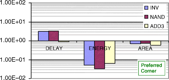
Figure 26.1 Median delay, energy, and area of proposed devices in NRI benchmark, normalized to ITRS 15 nm CMOS (courtesy of Kerry Bernstein) [3]
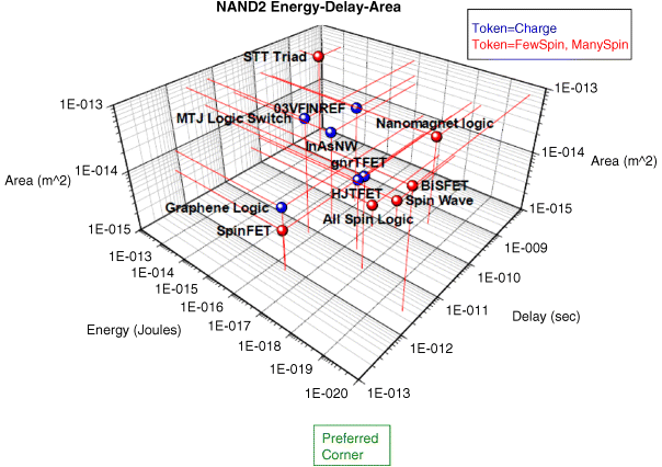
Figure 26.2 Area, energy, and delay of NAND2 gate of various postCMOS technologies from 2011 NRI benchmark (courtesy of Kerry Bernstein) [3]
Moving beyond the logic gate, it is important to understand the potential impact of the transport delay for the different information tokens these devices employ. As shown in Figure 26.3, communication with many of the noncharge tokens can be significantly slower than moving charge, although this may be balanced in some cases with significantly lower energy for transport. Moreover, the combination of the new balance between switch speed, switch area, and interconnect speed can lead to advantages in the span of control for a given technology. Finally, for some of the technologies, such as Nano-Magnetic Logic (NML), there is no strong distinction between the switch and the interconnect, indicating opportunities of novel architecture to exploit some of these attributes.
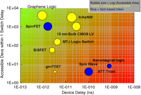
Figure 26.3 Transport impact on switch delay, size, and area of control. Circle size is logarithmically proportional to physically accessible area in one delay. Projections for 15 nm CMOS included as reference (courtesy of Kerry Bernstein) [3]
An independent study [4] showed disadvantages of spin-based devices in terms of speed without obvious energy advantage. However, it should be emphasized that the study is only based on active switching energy without considering other unique advantages of these devices for creative designs to reduce overall power consumption, for example, nonvolatility to eliminate standby power. This study also evaluated power-constrained throughput as an important parameter for low-power design.
At the architecture level, the ability to speculate how these devices will perform is still in its infancy. While the ultimate goal is to compare at a very high level – for example, how many MIPS can be produced for 100 mW in 1 mm2 – the current work must extrapolate from only very primitive gate structures. One initial attempt to start this process has been to look at the relative “logical effort” [9] for these technologies, a figure of merit which ties fundamental technology to a resulting logic transaction. Several of the devices appear to offer advantage over CMOS in logical effort, particularly for more complex functions, which increases the urgency of joint device–architecture co-design for emerging technologies.
26.2.3 Observations and Perspectives
A number of common themes have emerged from these benchmark studies [10,11].
- The energy–delay tradeoff conundrum will continue to be a challenge for all devices. Getting to low voltage remains a priority for achieving low power, but new approaches to improve throughput with “slow” devices need to be developed.
- Most of the architectures considered to date in the context of new devices utilize binary logic to implement von Neumann architecture. In this area, CMOS implementations are very competitive across the spectrum of energy, delay and area – not surprising since these architectures have evolved over several decades to exploit the properties and limitations of CMOS. Novel electron-based devices – which can include devices that take advantage of collective and nonequilibrium effects – appear to be the best candidates as a drop-in replacement for CMOS for binary logic applications.
- As the behavior of other emerging research devices becomes better understood, work on novel architectures that leverage these features will be increasingly important. A device that may not be competitive at doing a simple NAND function may have advantages in doing a complex adder or multiplier instead. Understanding the right building blocks for each device to maximize throughput of the system will be critical. This may be best accomplished by thinking about the high-level metric a system or core is designed to achieve (e.g., computation, pattern recognition, FFT, etc.) and finding the best match between the device and circuit for maximizing this metric.
- Increasing functional integration and on-chip switch count will continue to grow.
- Patterning, precise layer deposition, material purity, dopant placement, and alignment precision critical to CMOS will continue to be important in new device architectures.
- Assessment of novel switches must also include the transport mechanism for the information tokens. Fundamental relationships connecting information generation with information communication spatially and temporally will dictate CMOS' successor.
Based on the current data and observations, it is clear that CMOS will remain the primary basis for IC chips for the coming decade. While it is unlikely that any of the current emerging devices could entirely replace CMOS, several do seem to offer advantages, such as ultra-low power or nonvolatility, which could be utilized to augment CMOS or to enable better performance in specific application spaces. One potential area for entry is special-purpose cores or accelerators that could off-load specific computations from the primary general-purpose processor and provide overall improvement in system performance. This is particularly attractive given the move to multi-core chips. These would include specific, custom-designed cores dedicated to accelerate high-value functions, such as accelerators already widely used today in CMOS (e.g., encryption/decryption, compression/decompression, floating point units, digital signal processors, etc.), as well as potentially new, higher-level functions (e.g., voice recognition). While integrating dissimilar technologies and materials is a big challenge, advances in packaging and 3D integration may make this more feasible over time.
An accelerator using a non-CMOS technology would likely need to offer an order of magnitude performance improvement relative to its CMOS implementation to be considered worthwhile. That is a high bar, but there may be instances where the unique characteristics of emerging devices, combined with a complementary architecture, could be used in implementing a particular function. At the same time, the changing landscape of electronics (moving from uniform, general purpose computing devices to a spectrum of devices with varying purposes, power constraints, and environments spanning servers in data centers to smart phones to embedded sensors) and the changing landscape of workloads and processing needs (Big Data, unstructured information, real-time computing, 3D-rich graphics) are increasing the need for new computing solutions. One of the primary goals then for future beyond-CMOS work should be to focus on specific emerging functions and optimize between the device and architecture to achieve solutions that can break through the current power/performance limits.
26.3 Survey-based Critical Assessment of Emerging Devices
26.3.1 Overall Technology Requirements and Relevance Criteria
The second method for benchmarking emerging memory and information processing devices is based on a survey in the ERD group. Some emerging devices are charge-based structures proposed to extend CMOS to the end of the current roadmap, also known as “CMOS extension.” Other emerging devices use charge as the information token but in a non-MOSFET device structure or even use an information token other than charge, known as “beyond-CMOS.” A set of relevance or evaluation criteria are used to parameterize the extent to which proposed “CMOS extension” and “beyond-CMOS” technologies are applicable to memory or information processing applications. The criteria include: (1) scalability, (2) speed, (3) energy efficiency, (4) gain (logic) or ON/OFF ratio (memory), (5) operational reliability, (6) operational temperature, (7) CMOS technological compatibility, and (8) CMOS architectural compatibility.
26.3.2 Methodology
Each CMOS extension and beyond-CMOS device is evaluated against these criteria. Performance potential for each criterion is assigned a value from 1 to 3, with “3” substantially exceeding ultimately scaled CMOS, and “1” substantially inferior to CMOS or a comparable existing memory technology. These numbers are more precisely defined in Table 26.1.
Table 26.1 Individual potential for emerging logic and memory devices related to each technology relevance criterion
| 3 | Substantially exceeds ultimately scaled CMOS or baseline memory (relevance criteria 1–5). (6) or is compatible with CMOS or baseline memory operating temperature. (7) or is monolithically integrable with CMOS or baseline memory wafer technology. (8) or is compatible with CMOS or baseline memory wafer technology. |
| 2 | Comparable to ultimately scaled CMOS or baseline memory (relevance criteria 1–5). (6) or requires a very aggressive forced air cooling technology. (7) or is functionally integrable (easily) with CMOS or baseline memory wafer technology. (8) or can be integrated with CMOS or baseline memory architecture with some difficulty. |
| 1 | Substantially (2×) inferior to ultimately scaled CMOS or baseline memory (relevance criteria 1–5). (6) or requires very aggressive liquid cooling technology. (7) or is not integrable with CMOS or baseline memory wafer technology. (8) or cannot be integrated with CMOS or baseline memory architecture. |
26.3.3 Results of the Survey-based Critical Assessment
The critical review results for the memory and logic devices produced both numerical evaluations based on the criteria above and more qualitative evaluations of the current critical issues and ultimate potential. The review results are plotted in spider charts in Figures 26.4 to 26.7. Some of the qualitative factors are interpreted briefly below.
26.3.3.1 Emerging Research Memory Technologies
In Ferroelectric FET memory, a ferroelectric dielectric forms the gate insulator of a FET. The main concern for FeFET memory lies in operation reliability. Operational reliability of the FeFET memory is limited by the time dependent remnant polarization of the ferroelectric gate dielectric, reflected in retention loss. Control of the ferroelectric–semiconductor interface is critical for FeFET properties. The scalability of FeFET memory beyond the 22 nm generation is uncertain (please refer to Chapter 6 in this book for details).
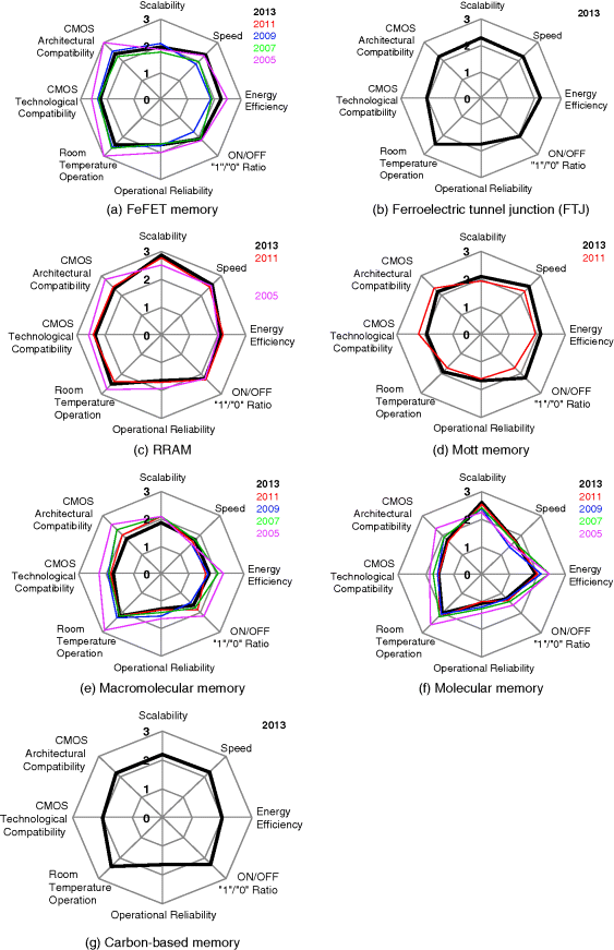
Figure 26.4 Technology performance evaluation for (a) FeFET memory, (b)ferroelectric tunnel junction (FTJ), (c) RRAM, (d) Mott memory, (e) macromolecular memory, (f) molecular memory, and (g) carbon-based memory
In ferroelectric tunnel junction (FTJ) memory, the device is controlled by the ferroelectric polarization of a tunnel barrier. With a simple two-terminal structure, FTJ is expected to have better scalability than FeFET. Ferroelectric thin film seems to maintain ferroelectric properties down to a couple of nm. Overall, FTJ has very similar performance rating as FeFET, because of the common underlying material property and device physics (please refer to Chapter 9 in this book for details).
RRAM includes multiple device types and mechanisms with varying level of maturity. The survey is based on rating of the general field rather than specific types. Some recent breakthroughs in RRAM significantly enhanced perceived potential of this technology, for example, 32 Gb array demonstration [12]. Overall RRAM assessment is similar or better than existing CMOS-based nonvolatile memories (Flash). An advantage of RRAM is scalability owing to the filamentary conduction and switching mechanisms. The simple device structure and fabrication-friendly materials also contribute to high rating in CMOS compatibility. One of the major concerns of RRAM is the operation reliability due to stochastic nature and defect-related mechanisms. Large variation of RRAM switching parameters has been commonly observed and is considered an intrinsic feature of RRAM mechanisms (please refer to Chapter 8 in this book for details).
Mott memory is one of the electronic-effect resistive switching memories, which is believed to have a fast switching speed. Important challenges include operation temperature and reliability. Depending on whether the conditions that triggers the transition are sustained after switching, the resistance change may or may not be nonvolatile (please refer to Chapter 9 in this book for details).
Carbon-based memory includes different types of carbon materials (carbon nanotube, graphene, amorphous carbon, etc.), which may also vary widely in maturity. Carbon-based memory is generally perceived to have similar or better performance than Flash memory except for reliability. Lack of clear understanding of the operation mechanisms in these devices makes it difficult to predict or improve their reliability.
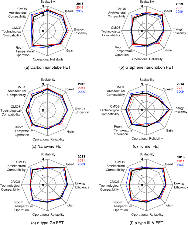
Figure 26.5 Technology performance evaluation for (a) carbon nanotube FET, (b) graphene nanoribbon FET, (c) nanowire FET, (d) tunnel FET, (e) n-type Ge FET, and (f) p-type III-V FET
Neither of the last two memory technologies evaluated, Macromolecular Memory and Molecular Memory, is considered to have long range potential for high-performance computing due to low expectations for speed, operational reliability, and Ion/Ioff ratio (please refer to Chapters 10 and 11 in this book for details).
26.3.3.2 Emerging Research Logic Technologies
Nanowire FETs offer an appealing approach to scale CMOS with attributes similar to Carbon nanotube (CNT) FETs, including excellent gate control of the channel and reduced short channel effects. Nanowire FETs also have challenges similar to those for CNTs related to well controlled growth, placement and fabrication as well as parasitic resistances and capacitances.
CNT FETs offer high carrier mobility, high quasi-ballistic charge carrier velocity, and a tubular structure ideally suited for minimized short channel effects (i.e., abrupt turnoff of channel current), if a gate all around process is developed. Other challenges include the ability to obtain single wall semiconducting nanotubes, control the bandgap energy, control growth of nanotube position/direction, and control the carrier type and density (please refer to Chapter 16 in this book for details).
The tunnel FET offers an appealing concept for substantially lowering the energy dissipated in a switching device by substituting a tunneling process for a thermionic process for injecting charge carriers into the channel of a MOSFET. The major challenge is to simultaneously obtain a sharp subthreshold slope (much less than 60 mV/decade) with a high on-current, Ion. Furthermore the tunnel FET may have a problem with operational reliability due to high sensitivity to slight variations of the tunnel structure and the resulting tunnel barrier (please refer to Chapter 14 in this book for details).
While graphene nanoribbon (GNR) as a channel replacement material offers an attractive alternative, it faces several important challenges. Even assuming a solution to these materials and process challenges (including development of a viable epitaxial growth technology), GNR may not offer sufficient device gain to be competitive (please refer to Chapter 15 in this book for details).
The negative Cg MOSFET offers another approach to lower the energy dissipated in switching a MOSFET by utilizing negative capacitance in a MOSFET gate stack. The major challenge concerns identification of appropriate materials (ferroelectrics and/or oxides) that can provide the best voltage swing with minimal hysteresis. Another challenge comes from the integration of high-quality single-crystalline ferroelectric oxides on Si. Operational reliability may also be a concern for this device concept (please refer to Chapter 14 in this book for details).
The spin transistor category represents two different device structures. One is the spinFET and the other is the spin MOSFET. In both instances the device complements the usual field effect behavior of a MOSFET with additional functionality of magnetoresistive devices. Consequently, the spin transistors may enable more complex transfer functions with fewer devices than CMOS implementation. However, in spite of considerable focused research on these devices, none have been realized experimentally. In addition, there are concerns with the scalability, gain, operational reliability, and CMOS technological compatibility of these devices (please refer to Chapter 17 in this book for details).
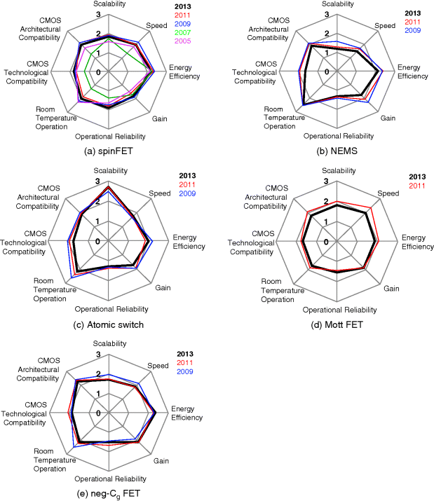
Figure 26.6 Technology performance evaluation for (a) spinFET, (b) NEMS, (c) atomic switch, (d) Mott FET, and (e) neg-Cg FET
The atomic switch is classified as an electrochemical switch using the diffusion of metal cations and their reduction/oxidation processes to form/dissolve a metallic conductive path. Both two-terminal and three-terminal devices have been developed. Switching speed, cyclic endurance, and uniformity need to be improved for general usage as a logic device. Establishment of clear device physics is one of the most important issues. In addition, development of the architecture to utilize the nonvolatility of these devices is desired.
The bilayer pseudo-spin field effect transistor (BiSFET) is a recently proposed concept for an ultra-low-power and fast transistor based on the possibility of a room temperature exciton (paired electron and hole) superfluid condensate in two oppositely charged (n-type and p-type) layers of graphene separated by a thin dielectric. So far, the device has remained at conceptual stage. Fabrication of BiSFETs with the necessary degree of control of graphene, dielectric and surface quality, and alignment imposes great challenges.
All spin logic (ASL) utilizes magnets to encode binary information and operates via spin current. Spin injected by a magnetic contact drives the switching of another magnet in the next stage. The concept has attracted attention due to progress in spin-based materials and devices (please refer to Chapter 17 in this book for details).
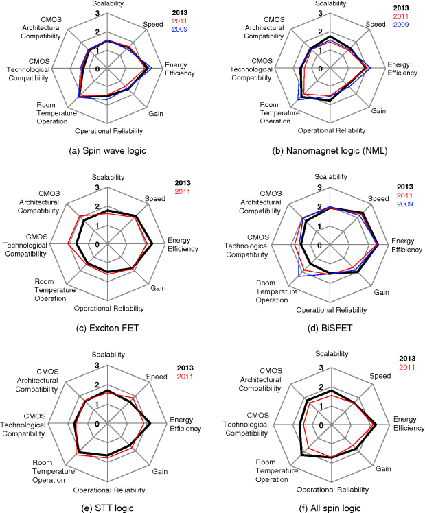
Figure 26.7 Technology performance evaluation for (a) spin wave logic, (b) nanomagnet logic (NML), (c) exciton FET, (d) BiSFET, (e) STT logic, and (f) all spin logic
The Mott field effect transistor (Mott FET) utilizes a phase change in a correlated electron system induced by a gate voltage as the fundamental switching paradigm. It could have a similar structure as conventional semiconductor FETs, with the semiconductor channel replaced by correlated electron materials. Besides electric field excitation, the Mott phase transition can also be triggered by photo- and thermal excitations for potential optical and thermal switches. Challenges with Mott FETs include fundamental understanding of gate oxide-functional oxide interfaces and local energy bandstructure changes in the presence of electric fields (please refer to Chapter 14 in this book for details).
Micro/Nano-Electro-Mechanical (M/NEM) switches (or relays) are based on the displacement of a solid beam under the influence of electrostatic force in order to create a conducting path between two electrodes. Ideally, M/NEM relays feature two key properties for logic computation which are unavailable in MOSFETs: zero leakage and zero subthreshold swing. The most important issue with M/NEM relays is nanoscale contact reliability. High impact velocity at the end of pull-in and the resultant “tip bouncing” (which also increases the effective switching delay) can aggravate the problem. The presence of surface forces (van der Waals or Casimir) can cause sticking and switching failure. Scaling is another concern for M/NEM relays. At gaps of a few nm, the subthreshold swing is expected to degrade due to the onset of tunneling current. With sufficiently small dimensions and gaps, the effect of Brownian beam motion may become significant (please refer to Chapter 18 in this book for details).
The other spintronics devices, spin wave devices and nanomagnetic logic, are viewed to be very early in their development or as being limited by important challenges related to their projected speed, gain, operational reliability, and CMOS technological compatibility.
26.3.3.3 Observations and Perspectives Based on the ERD Survey
Several new, nonvolatile memory technologies are emerging as attractive candidates to supplement or perhaps to eventually replace Flash memories. These memory device technologies are also stimulating research efforts to explore new applications.
- Charge-based FET and FET-like devices (e.g., nanowire FETs, III-V and/or Ge alternate channel material MOSFETs, carbon-based alternate channel MOSFETs, homojunction and heterojunction tunneling FETs) may enable extension of CMOS scaling in standard binary digital von Neumann applications.
- Spin-based devices offer lower dynamic switching energy and smaller device area compared to silicon CMOS. However these advantages come at a cost of slower speed. An important advantage of some spin devices is their ability to perform complex circuit functions with fewer devices than CMOS implementations. Successful execution of this strategy could allow increased device densities on the die.
- Nonvolatility of some emerging logic devices may be utilized in low-power designs. This advantage is not yet quantified in the benchmark results. Innovative architecture designs are needed to fully utilize this unique property.
26.4 Retrospective Assessment of ERD Tracked Technologies
The value of ERD's technology evaluation activities is estimated by the extent to which ERD transfers new Potential Solutions to other ITRS topical areas [for example, PIDS (Process, Integration, Devices, and Structures) and FEP (Front End Processes)]. Impact is also judged by transfer of evaluated technologies entries to one or more semiconductor companies.
Contributions of value to the semiconductor industry can be both direct and indirect. Direct influence is achieved through the transfer of maturing technologies from ERD to PIDS and to FEP (Tables 26.2–26.5). The acceptance by PIDS and/or FEP of a technology entry recommended by ERD sends an important message to the tool supplier community that they may need to begin R&D activities in preparation to meet their customers' eventual needs.
Table 26.2 Emerging memory devices evaluated by ERD
| Memory device | Year accepted | Year transitioned/removed | Transitioned to PIDS? | Transitioned to Manufacture? | |
| Yes | No | ||||
| Phase change | 2001 | 2005 | X | Yes | |
| Magnetic RAM | 2001 | 2011 (STT-MRAM) | X | Yes | |
| Floating body DRAM | 2001 | 2005 | X | ||
| Floating nano-gate NVRAM | 2001 | 2007 | X | ||
| Engineered tunnel barrier NVRAM | 2005 | 2009 | X | ||
| Single/few electron transistor DRAM | 2001 | 2005 | X | ||
| Insulator resistance change | 2003 | 2007 | X | ||
| ReRAM | 2011 | ||||
| – Electrochemical (chemical bridge) | 2007 | 2011 | X | ||
| – Fuse/anti-fuse (nanothermal) | 2007 | 2011 | X | ||
| – Valence change (nanoionic) | 2007 | 2011 | X | ||
| Electronic effects RAM | 2007 | 2011 | X | ||
| Nanomechanical NVRAM | 2007 | ||||
| Molecular RAM | 2001 | ||||
| Polymer RAM | 2005 | ||||
| Ferroelectric FET RAM | 2005 | 2011 | X | ||
| Ferroelectric RAM | 2011 | ||||
| Mott memory | 2011 |
Table 26.3 Extending nonclassical CMOS to the end of the roadmap – technology entries evaluated by ERD
| Logic or information processing device | Year accepted | Year transitioned/removed | Transitioned to PIDS? | Transitioned to manufacture? | |
| Yes | No | ||||
| Ultrathin body SOI | 2001 | 2005 | X | Yes | |
| Strained silicon (band engineered CMOS) | 2001 | 2005 | X | Yes | |
| Vertical CMOS | 2001 | 2005 | X | ||
| Multiple gate CMOS | 2001 | 2005 | X | Yes | |
| Schottky source/drain | 2003 | 2005 | X | ||
| CNT FET | 2001 | ||||
| GNR FET | 2009 | ||||
| Nanowire FET | 2003 | ||||
| III-V channel MOSFET | 2007 | 2011–2013 | X | ||
| Ge channel MOSFET | 2007 | 2011–2013 | X | ||
| Tunnel MOSFET | 2009 |
Table 26.4 Charge-based nonconventional beyond CMOS – nonFET devices and other charge-based information carrier devices – technology entries evaluated by ERD
| Logic or information processing device | Year accepted | Year transitioned/removed | Transitioned to PIDS? | Transitioned to manufacture? | |
| Yes | No | ||||
| Spin FET/spin MOSFET | 2001 | ||||
| IMOS | 2009 | ||||
| NEMS | 2009 | 2013 | X | ||
| Mott FET | 2011 | ||||
| Atomic switch | 2009 | ||||
| Negative Cg FET | 2009 | ||||
| RTD FET | 2001 | 2009 | X | ||
| E:QCA | 2001 | 2009 | X | ||
| SET | 2001 | 2011 | X |
Table 26.5 Alternative information processing devices – technology entries evaluated by ERD
| Logic or information processing device | Year accepted | Year transitioned/removed | Transitioned to PIDS? | Transitioned to manufacture? | |
| Yes | No | ||||
| RSFQ | 2011 | 2007 | X | ||
| Nanomagnetic logic (coherent spin devices) | 2009 | ||||
| Pseudospintronic (BiSFET) | 2009 | ||||
| Spin wave (collective spin devices) | 2009 | ||||
| Excitonic FET | 2011 | ||||
| All spin logic | 2011 | ||||
| Spin torque majority gate | 2011 | ||||
| Moving domain wall | 2007 | 2011 | X |
Indirect impact is also achieved through other avenues. For example, the chapter is used by several universities in teaching courses in nanoelectronics. University researchers are also aware of the key scientific and technological issues identified by the industry and ERD as gating acceptance of their new technology for further exploration and potential commercialization. In addition some international government agencies use the findings and recommendations of ERD as input to their research planning, funding, and execution decisions.
Tables 26.2–26.5 list all technology entries evaluated by ERD from 2001 to 2013, and illustrate their outcomes as to whether or not they were recommended for transfer to PIDS and FEP. For example, of the 12 memory technologies, shown in Table 26.2 as having been transitioned, four were transferred to PIDS, three re-classified under ReRAM, one re-classified as Mott RAM, and four were dropped. Two of the four technologies transferred to PIDS and FEP are in manufacture. An additional five memory technologies, including ReRAM and its component technologies, remain under active evaluation.
Tables 26.3–26.5 represent technology entries for logic and information processing that fall into three different classifications: (1) extending nonclassical CMOS, (2) charge-based nonFET devices, and (3) noncharge-based alternative information processing devices. Of the 28 technology entries in these three tables, a total of 13 have been transitioned out. Five of them, including ultra-thin body SOI, strained Si, multiple-gate CMOS (trigate, MUGFET, FinFET), III-V n-channel MOSFET, and Ge p-channel MOSFET, were transferred to PIDS and FEP; three of these technologies are currently in manufacture.
References
- 1. Zhirnov, V.V., Cavin, R.K., Hutchby, J.A., and Bourianoff, G.I. (2003) Limits to binary logic scaling – a gedanken model. Proceedings of the IEEE, 91(11), 1934–1939.
- 2. Bernstein, K., Cavin, R.K., Porod, W. et al. (2010) Device and architecture outlook for beyond CMOS switches. Proceedings of the IEEE, 98(12), 2169–2184.
- 3. Bernstein, K. (2011) NRI architecture benchmarking study phase 1.5 metrics readout – overview. NRI Annual Review.
- 4. Nikonov, D.E. and Young, I.A. (2013) Overview of beyond-CMOS devices and a uniform methodology for their Benchmarking. Proceedings of the IEEE, 101(12), 2498.
- 5. Keyes, R.W. (1979) The evolution of digital electronics towards VLSI. IEEE Transactions on Electron Devices, 26 (4), 271–279.
- 6. Matzke, Doug. (1997) Will physical scalability sabotage performance gains? IEEE Computer, 30(9), 37–39.
- 7. Welser, J. and Bernstein, K. (Jun 2011) Challenges for post-CMOS devices & architectures, IEEE Device Research Conference Technical Digest (Santa Barbara, CA), pp. 183–186.
- 8. Theis, T.N. and Solomon, P.M. (2010) Quest of the ‘Next switch’: prospects for greatly reduced power dissipation in a successor to the silicon field-effect transistor. Proceedings of the IEEE, 98(12), 2005–2014.
- 9. Sutherland, I. et al. (Feb. 1999) Logical effort: design fast CMOS circuits, 1st edn, Morgan Kaufmann, San Mateo, CA, ISBN: 10:1558605576.
- 10. Bourianoff, G. et al. (May 2008) “Boolean logic and alternative information-processing devices,” Computer, pp. 38–46.
- 11. Bourianoff, G., Brillouët, M., Cavin, R.K., Jr III et al. (2010) An extremely valuable collection of different approaches to post-CMOS technology. Proceedings of the IEEE, 98(12), 441–448.
- 12. Liu, T.Y. et al. (2013) “A 130.7 mm2 2-layer 32 Gb ReRAM memory device in 24nm technology,” ISSCC, pp. 210–212.