
19
Atomic Switch
Tsuyoshi Hasegawa and Masakazu Aono
WPI Center for Materials Nanoarchitectonics, National Institute for Materials Science, Japan
19.1 Chapter Overview
An atomic switch is a nanoionic device that controls the diffusion of metal ions and their reduction/oxidation processes in a switching operation to form/annihilate a metal atomic bridge, which in an ON state is a conductive path between two electrodes. An atomic switch works as a nonvolatile device due to an operating mechanism that requires the reduction/oxidation reaction that each occur at opposite polarities of applied bias. Since metal atoms provide a highly conductive path even if their path size is on the nanometer scale, atomic switches may enable downscaling to smaller dimensions than the 11 nm technology node.
The operation of an atomic switch was first demonstrated using a two-terminal structure, which is now widely used in applications for memories and programmable switches. Three-terminal operation was also demonstrated recently, in which the formation and annihilation of a conductive path between two electrodes is controlled by the third electrode. Three-terminal operation shows the potential for the use of atomic switches as logic devices.
The novel characteristics of atomic switches, such as their small size, low power consumption, low ON resistance and nonvolatility, will be useful in the development of future computing systems, such as nonvolatile logic systems and normally OFF computers. Novel functions have also been developed in atomic switches, including learning abilities, photo-sensing abilities, memristive operations, and synaptic functions. These novel functions are expected to contribute in the development of new types of neural computing systems.
In this chapter, the historical background, fundamentals such as operating mechanisms and characteristics, the various types and functions of atomic switches, the current state of the art, and future research directions are introduced.
19.2 Historical Background of the Atomic Switch
Precipitation of metal atoms from solid electrolytes, which was first reported more than 400 years ago [1], is a well-known phenomenon that has been studied extensively since the Faraday era [2]. Electronic devices that use electrochemical phenomena in their operation have been developed since the 1970s. For instance, Ag filament formation/dissolution was controlled on a surface of Ag-doped As2Se3 to make/annihilate a conductive path between the Ag electrode and the Au electrode formed on the surface [3]. During the same period, some devices were commercialized under the product names “memoriode” and “couliode” [4]. However, the supra-performance of semiconductor transistors in the last half-century overshadowed the atomic switches that were developed earlier. The situation is now changing as the ultimate downscaling of semiconductor transistors approaches its limits, providing various opportunities for the development of emerging nanoelectronic devices, including atomic switches. In particular, the various functions and unique characteristics of the emerging devices have attracted much attention because of their potential use in developing conceptually new computing systems.
19.3 Fundamentals of Atomic Switches
In this section we briefly introduce the operation mechanism of atomic switches. Although atomic switches have various device structures, their whole operation is based on a solid electrochemical reaction. The operating mechanisms and characteristics of two basic two-terminal atomic switches, that is, the gap-type atomic switch and the gapless-type atomic switch, are also introduced so as to understand the operation mechanism and characteristics in detail.
19.3.1 Operation Mechanism of Atomic Switches
There are several types of resistive switches, such as those based on a unipolar thermochemical mechanism, a bipolar valence change mechanism, and a bipolar electrochemical metallization mechanism. Atomic switches are operated by the third such mechanism, that is, bipolar electrochemical metallization. Although atomic switches have various device structures, they all have a reversible electrode, such as Ag or Cu, from which metal cations are ionized and brought to a channel region facing a counter electrode. The metal cations are reduced to neutral metal atoms at the channel region, resulting in the formation of a conductive channel. In the turning-on process, positive bias is applied to cause electrochemical reactions, that is, oxidation of metal atoms at the surface of the reversible electrode and reduction of metal cations at the channel region. When negative bias is applied to the reversible electrode, reduced metal atoms in the channel region are re-ionized and brought back to the reversible electrode, where they are reduced and subsequently introduced into the reversible electrode.
The operating bias of atomic switches, which is required for causing the electrochemical reactions, depends on the materials of both the reversible electrode and the counter electrode, as well as the material of the ionic transfer material that includes a channel region. Because the electrochemical reactions are an activation process, switching time is a function of the bias used, and becomes exponentially shorter with increasing bias. Typical operating biases are in the 1–2 V range when metal oxide is used as the ionic transfer material. Switching times in the few nano-second range have been demonstrated.
One of the characteristics that gives atomic switches an advantage over other devices is the potential for downscaling their device size to dimensions smaller than the 11 nm technology node. This is because metal atoms can make highly conductive channels, even though their size is on the nanometer scale.
In the following sections, the operation mechanism and characteristics of atomic switches are introduced in detail for each type of atomic switch.
19.3.2 Gap-type Atomic Switch
The gap-type atomic switch has a nanogap between a metal electrode facing an opposite ionic conductive material, formed on a reversible electrode. Operation of a gap-type atomic switch, that is, the controlled formation and annihilation of a metal atomic bridge in a nanogap, was demonstrated in 2001 using Ag2S as the ionic conductive material [5], as schematically shown in Figure 19.1. This gap-type atomic switch has two key points; the first is its use of an ionic and electronic mixed conductor as the ionic conductive material, which contains metal cations to be precipitated to form a metal atomic bridge in the nanogap. The electrical conductivity of the ionic conductive material is required to achieve low resistance in the ON state, which is measured electrically by flowing a current in a circuit. The second key point is its use of a tunneling current flowing in the nanogap, which can cause the chemical reaction necessary for precipitating metal atoms. The nanogap also ensures high resistance in the OFF state.
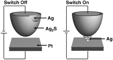
Figure 19.1 Schematic illustration of a gap-type atomic switch
The operating mechanism of this gap-type atomic switch is schematically shown in Figure 19.2. When a positive bias voltage is applied to the reversible electrode, metal atoms are oxidized and introduced from the electrode into the ionic conductive material as metal cations. The metal cations in the ionic conductive material migrate towards the surface, and are reduced by electrons tunneling from the counter metal electrode. The reduced metal atoms form a bridge between the ionic conductive material and the counter metal electrode, resulting in the turning on of the gap-type atomic switch.

Figure 19.2 Operating mechanism of a gap-type atomic switch
Application of a bias voltage with an opposite polarity causes the re-ionization of the precipitated metal atoms. The ionized metal atoms, that is, cations, are re-dissolved into the ionic conductive material, resulting in annihilation of the metal atomic bridge, as a result of which the gap-type atomic switch is turned off.
As shown in Figure 19.3, the electrochemical potential changes in the switching due to the diffusion of metal cations and the applied bias, resulting in the observed precipitation and re-ionization. This phenomenon can be caused by using various ionic conductive materials, with actual operations of gap-type atomic switches having been demonstrated using Ag2S [5,6], Cu2S [7], RbAg4I5 [8], and CuI.
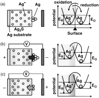
Figure 19.3 Reduction/oxidation processes induced by change in electrochemical potential due to the diffusion of metal cations in an ionic conductive material
The switching time of the gap-type atomic switch is a function of the applied bias voltage and temperature [6–8]. This becomes exponentially shorter with increases in the applied bias voltage, as shown in Figure 19.4. In most cases, two slopes are observed in the bias voltage versus the switching time, the cause of which has been explained in terms of the electrochemical nucleation of metal clusters at the surface of the ionic conductive material [8] and/or diffusion of metal cations in the ionic conductive material [7].
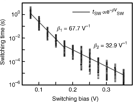
Figure 19.4 Switching time versus switching bias of a gap-type atomic switch
It would be an issue if gap-type atomic switches required an ionic conductive material, such as solid-electrolyte (Ag2S, etc.), since these materials are not compatible with the Complementary Metal Oxide Semiconductor (CMOS) process. One solution is to fabricate sulfide-based atomic switches on the top-most layer of CMOS devices [9]. Using this solution would be advantageous in such things as synaptic functions, memristive operations, and photo-sensing. Another unique characteristic of the gap-type atomic switch is conductance quantization, with a unit of 2e2/h, which occurs even at room temperature [6].
19.3.3 Gapless-type Atomic Switch
The gapless-type atomic switch operates by forming and dissolving a conductive path in an ionic conductive material, which is sandwiched by a reversible electrode and an inert electrode, as shown in Figure 19.5. The ionic conductive material of the gapless-type atomic switch should have less electrical conductivity because its OFF resistance is determined by the resistance of the ionic conductive material. In operation, the inert electrode works as a blocking electrode for diffusing metal cations, resulting in the precipitation of metal atoms at the interface between the ionic conductive material and the inert electrode. The precipitated metal atoms grow a filament towards the reversible electrode, and the gapless-type atomic switch is turned ON when the filament reaches the reversible electrode. The operating mechanism has been confirmed by observing the filaments using Transmission Electron Microscopy [10–12]. Conductance quantization at room temperature [13] has also evidenced that the conductive path consists of metal atoms. Reversing the polarity of the applied bias voltage causes dissolution of the metal filaments, resulting in the turning off of the gapless-type atomic switch.
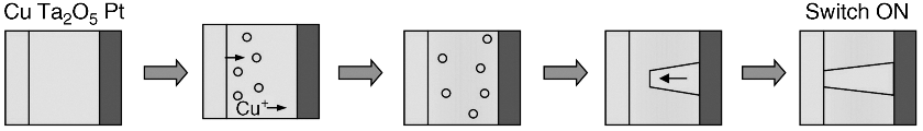
Figure 19.5 Operating mechanism of a gapless-type atomic switch
Gapless-type atomic switches using metal oxides as the ionic conductive material are believed to use a thermal effect in their turning-off process [14]. However, they only enable bipolar operation because the subsequent supply of metal cations thickens/rebuilds the metal filament, and thermal turning-off using the same polarity of the bias voltage is not possible in the operation of this type of atomic switch. This is in contrast to the fact that unipolar operation is enabled in devices such as phase change memories, as reviewed in Chapter 5, and fuse/antifuse memories [15], where a conductive path is ruptured by a thermal effect.
Operation of the gapless-type atomic switch has been demonstrated using many types of ionic conductive materials, including Ag2S [16], Cu2S [17] Ge0.3Se0.7 [18], Ta2O5 [19], HfO2 [20], SiO2 [21], TiO2 [22], CuOx [23], GeSbTe [24], ZrO2 [25], ZnO [26], WOx [27], and AgI [28].
In the case of the gapless-type atomic switch, switching time is determined by applied bias voltage, the diffusion constant of cations in the ionic conductive material, the activation energies for the reduction/oxidation processes, and temperature [29]. For instance, a conductive path should be formed between both ends of an ionic conductive material, the length of which is usually longer than a few nanometers, resulting in the switching time being dependent on the cation diffusion constant [30]. This is also the cause of the initial forming process usually required for gapless-type atomic switches. Here, “forming process” means that the application of a higher bias voltage, or the application of a bias voltage for a longer period of time, is required for the initial turning-on process than in the operation thereafter [31]. After the forming process, the performance of gapless-type atomic switches is good enough for them to be commercialized. For instance, switching times on the order of nanoseconds [32–34], cyclic endurance of over 1010 times [35,36], and retention times of over 10 years [37] have been achieved. Gapless-type atomic switches have been used as programmable switches in programmable logic devices [38] and as switches in crossbar-type logic circuits [39–41].
19.4 Various Atomic Switches
Various atomic switches and functions have been developed based on the operating mechanism of the basic atomic switches mentioned above. For instance, three-terminal atomic switches have been developed based on the gapless-type atomic switch, for use in nonvolatile logic systems. Unique functions, such as memristive operations and synaptic functions, have been developed based on both gap-type atomic switches and gapless-type atomic switches, which has enabled the development of new types of neuromorphic computers. In this section we introduce three-terminal atomic switches, memristive operations, synaptic functions, and the photo-sensing abilities of two-terminal atomic switches.
19.4.1 Three-terminal Atomic Switches
In the operation of three-terminal atomic switches, formation and annihilation of a conductive path between the source electrode and the drain electrode is controlled by the application of a gate bias to the gate electrode. Three-terminal atomic switches have an advantage in that the signal and control lines are separated, as in a semiconductor transistor, which drastically reduces their power consumption. The nonvolatility of atomic switches, along with the advantages offered by their low power consumption, offers a solution to issues inherent in conventional semiconductor transistors, by enabling the development of nonvolatile logic systems.
There are two types of three-terminal atomic switch: one based on filament growth and another based on the nucleation of metal clusters.
19.4.1.1 Three-terminal Atomic Switch Based on Filament Growth
The three-terminal atomic switch based on filament growth uses an electrochemical technique in which the reduction/oxidation of metal cations/atoms in an electrolyte (solution) is controlled by using a gate electrode. This technique is very common in electrochemistry; it was first used in the operation of a three-terminal atomic switch in 2004 [42] using AgNO3 + HNO3 as the electrolyte. In this example, Ag filament formation and dissolution were controlled between two Au electrodes dipped in the electrolyte. The technique has also enabled three-terminal atomic switch operation in a solid-electrolyte (Cu2S) [43], where Cu bridge formation and annihilation between the source electrode (Pt) and the drain electrode (Cu) was controlled by a gate electrode (Cu), as illustrated in Figure 19.6a. When a positive bias voltage was applied to the gate electrode, Cu+ cations were supplied into the Cu2S from the electrode by the oxidation of Cu atoms at the surface of the gate electrode, which is similar to the operation of a gapless-type atomic switch. Cu+ cations migrated towards the source and drain electrodes to be reduced at the two electrodes, resulting in formation of a bridge of Cu atoms between the source and the drain. When a negative bias voltage was applied to the gate electrode, Cu atoms were extracted from the atomic bridge as a result of their oxidation to Cu+ cations. The atomic bridge then became thinner and eventually disappeared. A typical operating result is shown in Figure 19.6b. In order to avoid the growth of a Cu bridge that reaches the gate electrode, the distance between the gate and the source/drain should be larger than that between the source and the drain. Although the three-terminal atomic switch uses Cu2S, which is not CMOS process compatible, the Cu2S-based three-terminal atomic switch can be used as a programmable switch in programmable logic devices by making them at the back end of the line of CMOS devices [44]. This circuit structure is similar to that in “CMOL” [45], which is a hybrid circuit combining CMOS stack and crossbar arrays with molecular-scale nanodevices at every crosspoint.
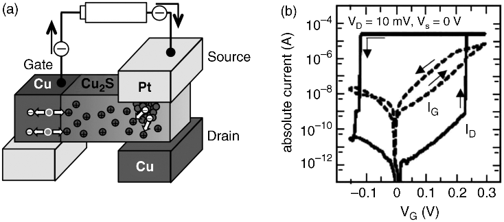
Figure 19.6 Three-terminal atomic switch controlling growth of a filament. (a) Schematic of the device. (b) Changes in drain current (ID) and gate current (IG) as a function of gate voltage (VG)
19.4.1.2 Three-terminal Atomic Switch Based on Nucleation Control
Another type of three-terminal atomic switch has been developed based on the nucleation control of metal clusters. Figure 19.7 shows the operating concept of this three-terminal atomic switch, in which metal cations brought from the gate electrode nucleate at the interface between the ionic conductive material and the source/drain electrodes, where the concentration of metal cations is at its highest. The key point of the development of this type of switch is the use of Ta2O5, which is an insulator in terms of electrical conductivity, as the ionic conductive material. Nucleation of metal clusters takes place when the concentration of metal cations, which is a function of the gate electrical field, reaches a certain threshold value, resulting in a drastic change in conductivity, that is, an insulator to conductive state transition. When the gate electrical field becomes smaller, the nuclei dissolve into metal cations moving towards the gate electrode to turn off the three-terminal atomic switch. The state variable of the three-terminal atomic switch based on nucleation control is a gate bias, which is the same as that of the conventional semiconductor transistor. Accordingly, this type of atomic switch is named the “atom transistor” [46]. This is in contrast to the three-terminal atomic switch based on filament growth, in which the state variable is a combination of a gate bias and a time.
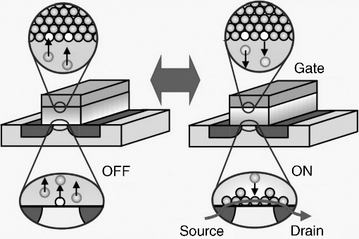
Figure 19.7 Three-terminal atomic switch controlling super-saturation induced nucleation
Another unique characteristic of the atom transistor is the dual functionality of selective volatile and nonvolatile operations, depending on the sweeping range of the gate bias.
Figure 19.8 shows such selective operations when Cu was used as the gate electrode material. When a gate bias (VG) was swept between 0 V and 1.5 V, the atom transistor showed volatile operation, where the drain current (ID) changed by six orders of magnitude in the VG range of 0.65–1.25 V, corresponding to a subthreshold slope of 100 mV/decade. On the other hand, two types of switching were observed when VG was swept to 3 V. First, switching occurred at VG = 1.4 V, where ID increased to the order of 10 μA, which is similar to the result shown in Figure 19.8a. Second, switching occurred at VG = 2.65 V, increasing the ID by another two orders of magnitude. Once the second switching occurred, the ON state was kept at VG = 0 V, requiring a negative VG application to turn off the atom transistor. The ON/OFF ratio in the nonvolatile operation is eight orders of magnitude larger. In both volatile and nonvolatile operations, the gate current (IG) remained small because Ta2O5 was used. The distribution of VG required for turning-on and turning-off, both for volatile and nonvolatile operation, is shown in Figure 19.9.
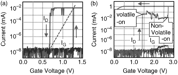
Figure 19.8 Operating results of an atom transistor: (a) volatile and (b) nonvolatile operations
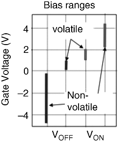
Figure 19.9 Ranges of bias voltage achieving volatile on/off and nonvolatile on/off oparations
Nonvolatile operation should be achieved by the nucleation of metal clusters, which accompanies the reduction/oxidation processes occurring with the application of a gate bias in the opposite polarity. One possible explanation for the volatile operation is that the metal cations themselves can make a conductive channel without nucleation when their concentration reaches a certain value. For instance, it has been reported that Ta2O5 lattices having a single Cuz+ cation in each unit cell is conductive [47]. In this case, decreasing VG causes redistribution of the metal cations, that is, moving of some cations toward the gate electrode, resulting in the disappearance of the conductive channel.
19.4.2 Novel Functions of Two-terminal Atomic Switches
In this section we introduce the novel functions of two-terminal atomic switches, that is, memristive operations, synaptic functions, and photo-sensing functions. These newly developed functions are expected to contribute in areas such as development of neuromorphic computers, rather than in improvements to present-day von Neumann computers.
19.4.2.1 Memristive Operations
The memristor, a two-terminal device, was predicted by L. Chua from the theoretical study of symmetries in electrical devices and circuits [48]. Although it was first introduced as an element that correlates magnetic flux ϕ and charge q, it is now understood to be a resistor having a memory effect [49], and is therefore referred to as a “Memristor.” In this generalized memristor, the resistance of the device changes depending on the history of input as well as the bias applied at the time. One of the operation modes of the memristor can be expressed as follows, that is, memresistance M(q) is a function of time-dependent charge q.
where ROFF/RON are resistance in the OFF/ON states respectively, μV is the average ion mobility, and D is the thickness of an ionic conductive material sandwiched between two electrodes.
Memristive operation has been achieved by various types of atomic switch. The first demonstration was achieved using an Ag/solid electrolyte/AgX (gapless-type atomic switch) system, in which resistance was controlled by increasing/decreasing the Ag cations in AgX [9]. Namely, the change in Ag to X ratio in AgX caused the change in the resistance of the system. Memristive operation has also been demonstrated in a gap-type atomic switch [50], in which the gap distance and/or thickness of an atomic bridge was controlled as the state variable.
The memristor can work as a synapse in neuromorphic systems as a single device, which has been achieved by using a complex circuit consisting of CMOS devices and analog devices. Synapses in neuromorphic systems are required to change their resistance, that is, synaptic weight, according to inputs from neurons in the system. This synaptic weight change has been shown using gapless-type atomic switches with the use of neurons made of CMOS-based circuits [51], where simple neuromorphic operations, such as the so-called “Pavlov's dog” operation [52], were demonstrated.
Because the number of synapses required in neuromorphic systems is much larger than that of neurons, the achievement of synaptic functions by a single device drastically reduces the size of neuromorphic systems and enables the development of highly integrated neuromorphic systems. Thus, in recent years, a variety of emerging devices, such as anion-based ReRAMs [53], ferroelectric devices [54], and phase change memories [55], have demonstrated memristive operations.
19.4.2.2 Self-controlled Synaptic Operation by Atomic Switches
Memory is believed to occur in the human brain as a result of two types of synaptic plasticity; short-term plasticity (STP) and long-term potentiation (LTP) [56]. Here, synaptic plasticity refers to changes that occur in the organization of the brain as a result of experience. STP is achieved through the temporal enhancement of a synaptic connection, which then quickly decays to its initial state. However, repeated stimulation causes a permanent change in the connection to achieve LTP; shorter repetition intervals enable efficient LTP formation from fewer stimuli, such as is schematically shown in Figure 19.10. This synaptic behavior is achieved in biological systems by the action potential from a neuron, which generates neuro-transmitters to change the strength of a synaptic connection.
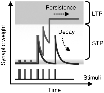
Figure 19.10 Memorization model based on the multi-store model
Conventional neuromorphic systems, such as those based on Spike Timing Dependent Plasticity (STDP), have been designed such that this synaptic weight change is fully controlled by signals from neurons. For instance, gradual change in short-term plasticity has been achieved by continuous or repeated application of an input bias, which is necessary because the synaptic devices developed so far require input whenever they change their resistance.
Recently, self-controlled synaptic operation was demonstrated using gap-type atomic switches, in which change in resistance occurred even after the end of signal input. Figure 19.11 shows synaptic behavior emulated by an Ag2S-based gap-type atomic switch [57], where STP was achieved with use of a lower pulse repetition input rate, and LTP was achieved with a higher pulse repletion input rate. The key point of this achievement is the use of small input pulses that do not singly turn on/off the Ag2S-based gap-type atomic switch. This synaptic operation was used to demonstrate concrete psychological behavior, in which new information from the external environment was stored as a sensory memory (SM) in the sensory register for a very short period of time, and then selected information was transferred from temporary short-term memory (STM) in the short-term store to permanent long-term memory (LTM) in the long-term store.
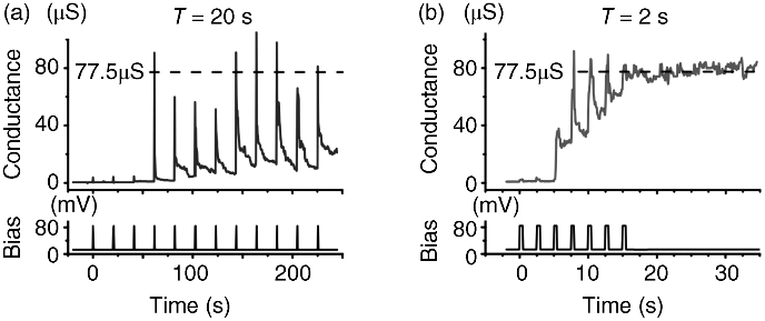
Figure 19.11 Changes in conductance of a gap-type atomic switch when input pulses were applied at intervals of 20 s (a) and 2 s (b)
This self-controlled synaptic operation has also been achieved using gapless-type atomic switches [13], showing a shorter time constant than that of gap-type atomic switches. These self-controlled synaptic operations do not require complex signals from neurons to control the synaptic weight, thus enabling the development of new types of neuromorphic systems with use of simple neurons.
19.4.2.3 Photo-sensing Ability of Atomic Switches
Gap-type atomic switches operate using tunneling current, which causes the precipitation of metal atoms in a nanogap. Using a wide gap (several tens of nm), in which tunneling current does not flow, and photo-conductive molecules within the wide gap, enables photo-sensing. As shown in Figure 19.12, light irradiation causes a photocurrent to flow between an ionic conductive electrode and a counter metal electrode applied with a certain bias voltage, resulting in the growth of a metal filament from the ionic conductive electrode. The photo-assisted atomic switch is turned on when the growing metal filament reaches the counter electrode. Since filament growth does not occur without the light irradiation, the photo-assisted atomic switch works as a photo-sensor with memory function and as well as a programmable switch, such as in an EPROM. The operation was first demonstrated using Ag2S as the ionic conductive material and N,N′-diheptylperylenetetracarboxylic diimide (PTCDI) as the photoconductive molecule [58]. The switching time of the photo-assisted atomic switch strongly depends on the gap size used, as shown in Figure 19.13. Other characteristics, such as the switching voltage, retention time, and ON/OFF ratio are similar to those of gap-type atomic switches. Cyclic endurance is an issue that needs to be investigated, because a metal filament can grow in and may subsequently cause damage to the photoconductive molecular layer.
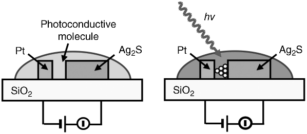
Figure 19.12 Photo-assisted atomic switch
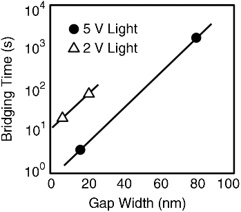
Figure 19.13 Switching time of the photo-assisted atomic switch
19.5 Perspectives
Atomic switches operate by controlling the formation and annihilation of a conductive path, made of metal atoms/cations, between two electrodes using a solid electrochemical reaction. There are several types of two-terminal atomic switch, that is, gap-type, gapless-type, and photo-assisted type. These have novel functions, such as memristive operations, synaptic functions, and photo-sensing with memory effect. Three-terminal atomic switches have also been developed. All such atomic switches have the potential to be downscaled beyond the 11 nm technology node. In addition to such novel functions and characteristics, development of fully CMOS compatible metal oxide-based atomic switches has attracted a great deal of attention as they gain importance as beyond-CMOS devices. For instance, because of their small size, nonvolatility and high ON/OFF ratio, two-terminal gapless-type atomic switches are expected to be the most promising candidates as programmable switches for next-generation Field Programmable Gate Arrays (FPGAs). The said characteristics are also suitable for their application to nonvolatile memory. Among the various atomic switches, the performance of two-terminal gapless-type atomic switches, shown in Table 19.1, have been much improved because of their potential for applications in the very near future. What will be more important for atomic switches is their application to beyond-von Neumann computers, such as nonvolatile logics and neural computers. Development of three-terminal atomic switches operated with a negative gate bias, corresponding to a p-type transistor, is needed to realize nonvolatile logics and to replace CMOS. The development of neuromorphic functions will also be more important in the research of atomic switches because the realization of neural computing systems is key to achieving both a drastic reduction in power consumption and the ability to perform highly complicated computations.
Table 19.1 Summary parameter table of the atomic switch (two-terminal gapless-type)
| Parameter | Status | Value for the device in this chapter |
| Cell size | Demonstrated | 10 nm |
| Projected | 5 nm | |
| Density | Demonstrated | 2.5E9/cm2 |
| Projected | 1E12/cm2 | |
| Device speed (reading/writing speed) | Demonstrated | <10 ns |
| Projected | <1 ns | |
| Operation voltages | Demonstrated | 0.6 V |
| Projected | <0.5 V | |
| Switching energy (set-current/reset-current) | Demonstrated | 1 μA/10 μA |
| Projected | Not known | |
| Endurance | Demonstrated | 1E6 |
| Projected | >1E11 | |
| Retention (for memory) | Demonstrated | 10 yr |
| Projected | >10 yr |
References
- 1. Ercker, L. (1951) Treaties on Ores and Assaying, 1574, (translated by Sisco A. G. and Smith C. S., Univ. Chicago, pp.) 177.
- 2. Faraday, M. (1833) On a new law of electric conduction. Philosophical Transactions of the Royal Society, 123, 507–515.
- 3. Hirose, Y. and Hirose, H. (1976) Polarity-dependent memory switching and behavior of Ag dendrite in Ag-photodoped amorphous As2S3 films. Journal of Applied Physics, 47, 2767–2772.
- 4. Ikeda, H. and Tada, K. (1980) Sanyo's Couliodes And Memoriodes, in Applications of Solid electrolytes (eds T. Takahashi and A. Kozaw), Academic Press, Cleveland, pp. 40–45.
- 5. Terabe, K., Hasegawa, T., Nakayama, T., and Aono, M. (2001) Quantum point contact switch realized by solid electrochemical reaction. Riken Review, 37, 7–8.
- 6. Terabe, K., Hasegawa, T., Nakayama, T., and Aono, M. (2005) Quantized conductance atomic switch. Nature, 433, 47–50.
- 7. Nayak, A., Tsuruoka, T., Terabe, K. et al. (2011) Switching kinetics of a Cu2S-based gap-type atomic switch. Nanotechnol, 22, 235201-1-7.
- 8. Valov, I., Sapezanskaia, I., Nayak, A. et al. (2012) Atomically controlled electrochemical nucleation at superionic solid electrolyte surfaces. Nature Materials, 11, 530–535.
- 9. Kaeriyama, S., Sakamoto, T., Sunamura, H. et al. (2005) A nonvolatile programmable solid-electrolyte nanometer switch. IEEE Journal of Solid-State Circuits, 40(1), 168–176.
- 10. Yang, Y., Gao, P., Gaba, S. et al. (2012) Observation of conducting filament growth in nanoscale resistive memories. Nature Communications, 3, 732.
- 11. Miao, F., Strachan, J.P., Yang, J.J. et al. (2011) Anatomy of a nanoscale conduction channel reveals the mechanism of a high-performance memristor. Advanced Materials, 23, 5633–5640.
- 12. Liu, Q., Sun, J., Lv, H. et al. (2012) Real-Time Observation on Dynamic Growth/Dissolution of Conductive Filaments in Oxide-Electrolyte-Based ReRAM. Advanced Materials, 24, 1844–1849.
- 13. Tsuruoka, T., Hasegawa, T., Terabe, K., and Aono, M. (2012) Conductance quantization and synaptic behavior in a Ta2O5-based atomic switch. Nanotechnol, 23, 435705-1-6.
- 14. Tsuruoka, T., Terabe, K., Hasegawa, T., and Aono, M. (2011) Temperature effects on the switching kinetics of a Cu-Ta2O5-based atomic switch. Nanotechnol, 22, 254013-1-1-9.
- 15. International Roadmap Committee (2009) International Technology Roadmap for Semiconductors, ITRS 2009 Edition, http://www.itrs.net/Links/2009ITRS/Home2009.htm (accessed 16 July 2013).
- 16. Kundu, M., Terabe, K., Hasegawa, T., and Aono, M. (2006) Effect of sulfurization conditions and post-deposition annealing treatment on structural and electrical properties of silver sulfide films. Journal of Applied Physics, 99, 103501-1-9.
- 17. Sakamoto, T., Sunamura, H., Kawaura, H. et al. (2003) Nanometer-scale switches using copper sulfide. Applied Physics Letters, 82, 3032–3034.
- 18. Soni, R., Meuffels, P., Petraru, A. et al. (2010) Probing Cu doped Ge0.3Se0.7 based resistance switching memory devices with random telegraph noise. Journal of Applied Physics, 107, 024517-1-10.
- 19. Sakamoto, T., Lister, K., Banno, N. et al. (2007) Electronic transport in Ta2O5 resistive switch. Applied Physics Letters, 91, 092110-1-3.
- 20. Haemori, M., Nagata, T., and Chikyow, T. (2009) Impact of Cu Electrode on Switching Behavior in a Cu/HfO2/Pt Structure and Resultant Cu Ion Diffusion. APEX, 2, 061401-1-3.
- 21. Schindler, C., Weides, M., Kozicki, M.N., and Waser, R. (2008) Low current resistive switching in Cu–SiO2 cells. Applied Physics Letters, 92, 122910-1-3.
- 22. Tsunoda, K., Fukuzumi, Y., Jameson, J.R. et al. (2007) Bipolar resistive switching in polycrystalline TiO2 films. Applied Physics Letters, 90, 113501-1-3.
- 23. Chen, A., haddad, S., Wu, Y. et al. (2005) “Non-Volatile Resistive Switching for Advanced Memory Applications,” in Tech. Dig., Int. Electron Devices Meet., pp. 765–768.
- 24. Aratani, K., Ohba, K., Mizuguchi, T. et al. (2007) “A Novel Resistance Memory with High Scalability and Nanosecond Switching,” in Tech. Dig. of the IEEE Int. Electron Devices Meet. pp. 783–786.
- 25. Li, Q., Dou, Ch., Wang, Y. et al. (2009) Formation of multiple conductive filaments in the Cu/ZrO2:Cu/Pt device. Applied Physics Letters, 95, 023501 1-3.
- 26. Yang, Y.C., Pan, F., Liu, Q., and Zeng, F. (2009) Fully Room-Temperature-Fabricated Nonvolatile Resistive Memory for Ultrafast and High-Density Memory Application. Nano Letters, 9, 1636–1643.
- 27. Kozicki, M.N., Gopalan, C., Balakrishnan, M., and Mitkova, M. (2006) A low-power nonvolatile switching element based on copper-tungsten oxide solid electrolyte. IEEE Transactions on Nanotechnology, 5, 535–544.
- 28. Guo, H.X., Yang, B., Chen, L. et al. (2007) Resistive switching devices based on nanocrystalline solid electrolyte (AgI)0.5(AgPO3)0.5. Applied Physics Letters, 91, 243513 1-3.
- 29. Valov, I., Waser, R., Jameson, J.R., and Kozicki, M.N. (2011) Electrochemical metallization memories—fundamentals, applications, prospects. Nanotechnol, 22, 254003 1-22.
- 30. Banno, N., Sakamoto, T., Iguchi, N. et al. (2008) Diffusivity of Cu ions in solid electrolyte and its effect on the performance of nanometer-scale switch. IEEE Transactions on Electron Devices, 55(11), 3283–3287.
- 31. Valov, I. and Kozicki, M.N. (2013) Cation-based resistance change memory. Journal of Physics D, 46, 074005-1-14.
- 32. Tsunoda, K., Kinoshita, K., Noshiro, H. et al. (2007) Diffusivity of Cu ions in solid electrolyte and its effect on the performance of nanometer-scale switch, Tech. Dig., IEEE Int. Electron Device Meet. pp. 767–770.
- 33. Schindler, C., Weides, M., Kozicki, M.N., and Waser, R. (2008) Low current resistive switching in Cu–SiO2 cells. Applied Physics Letters, 92, 122910 1-3.
- 34. M. N., Kozicki., Park, M., and Mitkova, M. (2005) Nanoscale memory elements based on solid-state electrolytes. IEEE Transactions on Nanotechnology, 4, 331–338.
- 35. Yang, J.J., Zhang, M.X., Strachan, J.P. et al. (2010) High switching endurance in TaOx memristive devices. Applied Physics Letters, 97, 232102-1-3.
- 36. Lee, M., Lee, C.B., Lee, D. et al. (2010) A fast, high-endurance and scalable non-volatile memory device made from asymmetric Ta2O5−x/TaO2−x bilayer structures. Nature Materials, 10, 625–630.
- 37. Banno, N., Sakamoto, T., Fujieda, S., and Aono, M. (2008) On-State Reliability Of Solid-Electrolyte Switch, Proc. of the Int. Reliabil. Phys. Symp., Phoenix, pp. 707–708.
- 38. Tada, M., Sakamoto, T., Tsuji, Y. et al. (2009) Highly Scalable Nonvolatile TiOx/TaSiOy Solid-electrolyte Crossbar Switch Integrated in Local Interconnect for Low Power Reconfigurable Logic, Tech. Dig. Int. Electron Devices Meet., pp. 943–946.
- 39. Heath, J.R., Kuekes, P.J., Snider, G.S., and Williams, R.S. (1998) A Defect-Tolerant Computer Architecture: Opportunities for Nanotechnology. Science, 280, 1716–1721.
- 40. Morales-Masis, M., van der Molen, S.J., Fu, W.T. et al. (2009) Conductance switching in Ag2S devices fabricated by in situ sulfurization. Nanotechnol, 20, 095710 1-6.
- 41. Borghetti, J., Snider, G.S., Kuekes, P.J. et al. (2010) ‘Memristive’ switches enable ‘stateful’ logic operations via material implication. Nature, 464, 873–876.
- 42. Xie, F.-Q., Nittler, L., Obermair, C., and Schimmel, T. (2004) Gate-Controlled Atomic Quantum Switch. Physical Review Letters, 93, 128303-1-4.
- 43. Banno, N., Sakamoto, T., Iguchi, N. et al. (2006) Solid-Electrolyte Nanometer Switch. IEICE Transactions on Electronics, E89-C(11), 1492–1498.
- 44. Sakamoto, T., Iguchi, N., and Aono, M. (2010) Nonvolatile triode switch using electrochemical reaction in copper sulfide. Applied Physics Letters, 96, 252104-1-3.
- 45. Strukov, D.B. and Likharev, K.K. (2005) CMOL FPGA: a reconfigurable architecture for hybrid digital circuits with two-terminal nanodevices. Nanotechnol, 16, 888–900.
- 46. Hasegawa, T., Itoh, Y., Tanaka, H. et al. (2011) Volatile/Nonvolatile Dual-Functional Atom Transistor. APEX, 4, 015204-1-3.
- 47. Gu, T., Tada, T., and Watanabe, S. (2010) Conductive Path Formation in the Ta2O5 Atomic Switch: First-Principles Analyses. ACS Nano, 4(11), 6477–6482.
- 48. Chua, L.O. (1971) Memristor - Missing Circuit Element. IEEE Transactions on Circuit Theory, CT-18, 507–519.
- 49. Strukov, D.B., Snider, G.S., Stewart, D.R., and Williams, R.S. (2008) The missing memristor found. Nature, 453, 80–83.
- 50. Hasegawa, T., Nayak, A., Ohno, T. et al. (2011) Memristive operations demonstrated by gap-type atomic switches. Applied Physics A, 102, 811–815.
- 51. Alibart, F., Gao, L., Hoskins, B.D., and Strukov, D.B. (2012) High precision tuning of state for memristive devices by adaptable variation-tolerant algorithm. Nanotechnol, 23, 075201-1-7, 075201.
- 52. Ziegler, M., Soni, R., Patelczyk, T. et al. (2012) An Electronic Version of Pavlov's Dog. Advanced Functional Materials, 22, 2744–2749.
- 53. Chang, T., Jo, S., and Lu, W. (2011) Short-Term Memory to Long-Term Memory Transition in a Nanoscale Memristor. ACS Nano, 5, 7669–7676.
- 54. Chanthbouala, A., Garcia, V., Cherifi, R.O. et al. (2012) A ferroelectric memristor. Nature Materials, 11, 860–864.
- 55. Wright, C.D., Hosseini, P., and Vazquez Diosdado, J.A. (2013) Beyond von-neumann computing with nanoscale phase-change memory devices. Advanced Functional Materials, 23, 2248–2254.
- 56. Bliss, T.V.P. and Collingridge, G.L. (1993) A synaptic model of memory: long-term potentiation in the hippocampus. Nature, 361, 31–39.
- 57. Ohno, T., Hasegawa, T., Tsuruoka, T. et al. (2011) Short-term plasticity and long-term potentiation mimicked in single inorganic synapses. Nature Materials, 10, 591–595.
- 58. Hino, T., Tanaka, H., Hasegawa, T. et al. (2010) Photo-assisted formation of an atomic switch. Small, 6, 1745–1748.