
13
Emerging Memory Devices: Assessment and Benchmarking
Matthew J. Marinella1 and Victor V. Zhirnov2
1Sandia National Laboratories, USA
2Semiconductor Research Corporation, USA
13.1 Introduction
We are at an interesting juncture in memory technology. As of the time of this writing, production NAND flash has been scaled to a critical dimension of 16 nm [1] and 3D Vertical NAND has entered commercial production [2]. However, endurance and retention have become strongly degraded as flash tunnel oxides become thinner, leading to requirements for extensive error correction code (ECC) schemes and substantial redundant storage requirements. Storage Class Memory (SCM) has identified the significant latency gap between NAND-based solid-state disks (SSDs) and DRAM [3,4] (SCM concepts are covered in detail in Chapter 25). Hence, an emerging or prototypical memory technology may supplement, or even supplant NAND flash in the coming decade. Furthermore, continued DRAM scaling faces numerous challenges, and does not yet have known manufacturable solutions past the 20 nm node [5]. Impending limitations of standard memory technologies combined with massive increases in data quantities have even led to proposals of a radical shift toward datacentric-based architectures such as nanostores [6].
Prototypical memory technologies, in particular spin transfer torque RAM (STT-RAM) and phase change RAM (PCRAM), have made improvements in recent years and are being commercially produced for niche markets. These technologies are discussed in detail in Chapter 4 (PCRAM) and Chapter 5 (STT-RAM) of this book. Emerging memory technologies, especially resistance switching memories (RRAM) have made rapid advancements in the past decade and offer the possibility of greater scaling and performance than prototypical or baseline technologies. Redox RAM (ReRAM) technologies have advanced at a particularly high rate in recent years, both in the scientific understanding and technological development of working prototype chips. ReRAM has been commercialized on a small scale [7,8], and multi-layered NAND-scale prototypes have been demonstrated [9,10]. In response to this increase in ReRAM research and development, the 2013 ITRS Emerging Research Devices (ERD) chapter added an expanded coverage of this technology, which is also reflected in this chapter. Other emerging memory technologies are further from commercialization but if certain challenges were overcome, these could offer additional benefits in energy, speed, and reliability.
Figure 13.1 provides a visual categorization of modern solid state memory technologies.1 A key distinguishing feature of these technologies is whether the technology requires an active power source to maintain data. If a technology loses data when the power source is removed, it is volatile, whereas if the information is retained without power it is nonvolatile. SRAM and DRAM are mature, volatile memory technologies whose key technological parameters, including critical dimensions, performance, and reliability have steadily advanced for several decades. NAND and NOR flash are mature nonvolatile memory (NVM) technologies that provide baseline performance, scaling, and reliability metrics against which prototypical and emerging memories are compared. Ferroelectric RAM (FeRAM or FRAM), PCM (or PCRAM), magnetic RAM (MRAM), and STT-RAM are prototypical technologies that have matured to the point that commercial products exist. When a technology reaches this stage, it is transferred from the ERD to the Process Integration, Devices, and Structures (PIDS) chapter of ITRS.
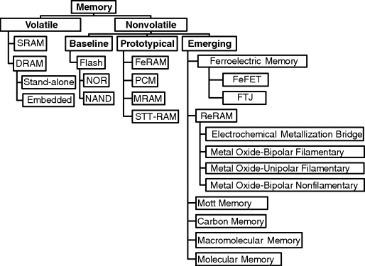
Figure 13.1 Taxonomy of memory technologies (adapted from the 2013 ITRS ERD chapter [5])
This chapter is written as a counterpart and expansion of the memory section of the ITRS Emerging Research Devices (ERD) chapter [5]. The intention is to provide a summary of the emerging memory technologies that fit the ITRS criteria,2 including an assessment of these technologies in the application space. Subsections 13.3 through 13.8 provides a brief overview of the physical principles governing the operation of each memory device, whereas more detailed information on physics can be found in the previous chapters of this book and external references. In addition, they summarize significant technological advancements of each technology in the past several years, as well as key research challenges. Finally, a comparative assessment of the collective group of emerging memory devices is made, with regards to the technological areas that emerging memories are most likely to compete in, namely NAND flash, SCM, and DRAM.
13.2 Common Emerging Memory Terminology and Metrics
All of the emerging memory technologies covered in this chapter are nonvolatile. Switching of a nonvolatile memory state is typically referred to as a either a SET or RESET operation. With the exception of the FeFET, all of the emerging memory technologies in Figure 13.1 are two terminal resistance switching devices (RRAM). For an RRAM cell, SET switching refers to the operation of changing from the high resistance state (HRS) to low resistance state (LRS). SET switching is also referred to as a “program” or “write” operation. The RESET operation (also referred to as “erase”) switches the device from the LRS to the HRS. The HRS and LRS can be considered “0” and “1” bit states, respectively. The LRS state also might be referred to as a SET state, and the HRS as the RESET state.
Nonvolatile memories typically are assessed by the following key metrics:
- Endurance: the number of SET/RESET cycles a memory can survive before the difference between the two states cannot be adequately determined by the read circuitry. Historically, flash has a maximum endurance of 105–106 cycles. Current ultra-scaled cells have an endurance of 103 or less [5].
- Retention: the amount of time a device will retain a state, as sensed by the array circuitry, after the programming bias is removed. This can be evaluated on a virgin device or one that has been fully cycled. As a baseline, flash historically is expected to have state retention of 10 years at 85 °C after cycling to maximum endurance (i.e., 105 cycles).
- Resistance ratio, ROFF/RON: The ratio of the HRS to LRS is an important metric, which needs to be large enough to avoid an overlap of the HRS and LRS distributions in an array. If these distributions overlap, it will lead to bit errors [11].
- Switching voltage, current, and power: SET and RESET switching voltages and currents are important metrics of a memory operation. Switching voltage and current are the primary factors determining the power, and hence heat generation in a densely packed memory array. Heating during switching can be the primary factor in determining how closely cells can be spaced. In addition, the switching current determines the size of drive transistor required. The maximum switching voltage determines the compatibility of BEOL technology with scaled CMOS. Most resistive memories switch with less than 3 V, whereas switching current ranges from nA to mA, and hence switching current is a common metric which is used to compare. In ReRAM, typically the RESET currents are highest, which is why this is a particular metric of importance.
- Switching time: The time which it takes to transition from SET to RESET or RESET to SET for a memory cell. This is an important metric for system speed. In fact the “memory bottleneck” due to limited speed of memory access is one of the difficult problems of modern and future information processing systems.
- Switching energy: Switching energy is the product of switching time and power. A memory's switching energy is a key performance metric for applications ranging from high performance to mobile computing.
With the exception of the FeFET, all of the emerging memory technologies in Figure 13.1 are two terminal resistance switching devices. This makes them amenable to an efficient crossbar configuration, where perpendicular top electrode and bottom electrode lines intersect at each device. This is the most dense possible arrangement, as each individual device only requires an area of 4F2, where F is the minimum areal feature size of the device. However, in order to avoid so-called sneak paths interfering with the read and write of the cell, it is necessary to have a select device isolating each device. Select device concepts and candidate structures are covered in detail in Chapter 12.
13.3 Redox RAM
The emerging memory technology category of Redox RAM (ReRAM) has seen the greatest increase in research activity over the past two years, with roughly 593 publications in the literature [5]. The terminology redox RAM was suggested in 2007 in Reference [12] to describe the category of resistance switching resulting from an electrochemical reaction involving oxidation and reduction processes in a thin insulating film sandwiched between two electrodes. Redox memory can be split into four major categories based on the physical mechanisms governing their behavior, as illustrated in Figure 13.2. It is quite useful to categorize ReRAM in terms of physical mechanisms, as done in Reference [12]. However, it is possible that there is some combination of these mechanisms in a structure, especially when fabricated with a metal oxide switching layer. Therefore in Figure 3.2 the three metal oxide categories have been named by the electrical behavior they exhibit – namely distinguished by bipolar versus unipolar operation, as well as whether or not the current through a device is strongly dependent on area. These four categories of ReRAM are described in the following sections.
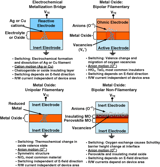
Figure 13.2 Description of the four categories of ReRAM
13.3.1 Electrochemical Metallization Bridge
Electrochemical metallization bridge (EMB) memory is also referred to as conducting bridge RAM (CBRAM) and programmable metallization cell (PMC) technology. A key attribute of EMB memory is that Switching is based on the motion of cations. An EMB type ReRAM consists of an asymmetric metal/insulator/metal structure with a reactive electrode composed of either Ag or Cu (see Figure 13.2). The inert electrode is chosen such that it will not strongly react with the insulator; typical choices are Pt, Ni, Au, and W. The insulator is often a solid electrolyte such as GeSe, GeS, a binary oxide, or a Cu-doped binary oxide (which are mixed conductors) [13]. A comprehensive table of EMB insulators is provided in Reference [14].
EMB switching is typically bipolar, and hence requires an electric field. Unipolar operation is also possible, but requires higher current and energy and is therefore uncommon [15,16]. Prior to the commencement of switching, an electroforming process is required to create an initial filament. Switching occurs based on the formation and dissolution of an Ag or Cu filament under an electric field. The filament oxides are formed based on the oxidation reaction (using Ag as an example) [13]:
The SET process occurs as the cations oxidize under the electric field and deposit on the inert electrode where they are reduced and form a filament. The RESET process involves dissolution of the filament initiated by high Joule heating at the thinnest portion of the filament, re-oxidizing the Ag. Then, electrochemical motion of the Ag+ cations causes the filament to disperse into the insulator, returning the structure to a high resistance state. The specific details of the process are still the subject of some debate, and are comprehensively reviewed in References [13,14,17].
EMB ReRAM technology has achieved significant performance metrics. Endurance as high as 1010 with little degradation was demonstrated in GeSe cells (projected to well beyond 1011 cycles) [18]. High temperature retention due to random diffusion of Ag or Cu atoms in the insulator has historically been considered a moderate weakness for EMB ReRAM. However, recent results show excellent retention, with states holding after 1000 h at 200 °C [19]. Scalability to dimensions of 20 nm has been demonstrated for a GeSe EMB cell [20]. A recent experiment demonstrating quantized conductance corresponding to the conductivity of a filament formed from a single chain of Ag atoms showed that scaling to atomic dimensions is possible [21].
Significant progress has been made in the development of EMB ReRAM macros and low density commercial products – which are important to foster advancement of an emerging technology [11]. In 2012, a 1 Mbit integrated EEPROM replacement chip with 0.18 μm technology was released [15]. Recently, a very low power prototype chip which switches at 600 mV and achieves a 1 pJ SET and 8 pJ RESET energy was demonstrated [22]. Also, a W/Al2O3/Ti/CuTe-based EMB cell realizing subnanosecond SET and RESET times was reported [16].
A fundamental research challenge of EMB is the understanding of subtle details of the switching process. Recent research in this area has elucidated many of the details of the switching physics, but the scientific community lacks complete agreement on the exact nature of the filament formation and dissolution process details. Another key research challenge for EMB ReRAM (and other filament-based ReRAM technologies) is random telegraph noise (RTN) [11]. This effect manifests itself as a variation in read current, especially in the high resistance state where the fluctuation of small numbers of atoms in the filament may vary to cause conductivity changes [23]. EMB ReRAM cells often employ a solid electrolyte switching layer (e.g., GeSe), which are not easy to integrate with a CMOS back end of line (BEOL) process and may be damaged by high temperatures. For this reason, commercial EMB products are generally integrated during later steps of the BOEL process, whereas it may be desirable for maximum performance to integrate the cell before the first metallization layer.
13.3.2 Metal Oxide: Bipolar Filamentary
The metal oxide bipolar filamentary (MO-BF) category of ReRAM is an asymmetric metal/insulator/metal structure, in which switching occurs due to the change of oxygen anion concentration in a filament (see Figure 13.2). This type of memory is often referred to as Valence Change Memory (VCM) in the literature due to the change of valence states of oxygen atoms during switching [12]. The switching material is typically a transition metal oxide; recently the most common materials are HfOx and TaOx due to CMOS compatibility, scalability, and performance. Other common switching oxides include TiO2, WOx, AlOx, as well as nitrides (AlN [24]), and oxynitrides (AlOxNy [25]). In addition, bilayer structures are often used with either two stoichiometries of the same oxide (e.g., Ta2O5−x/TaO2−x [26]), or with a second layer composed of a different oxide intended to enhance nonlinearity and act as a select device [27]. The ohmic electrode is typically fabricated from a material with high oxygen reactivity, such as Ta, Hf, or Ti. This electrode may serve as an oxygen reservoir. The inert electrode (which may also be referred to as the active electrode), is typically formed from a material that will not react significantly with the metal oxide, such as Pt, Ir, TiN, or TaN. Switching is thought to occur in the metal oxide region directly adjacent to the interface with this inert electrode.
As with other filamentary ReRAM, prior to the resistance switching process, an electroforming step is required. In the case of MO-BF ReRAM, the electroforming step does permanent damage [17], and has similarities to a “soft breakdown” of an oxide [11,28]. “Forming free” processes have been reported [29], although it is suggested that a filament forming process still occurs at a very low current [30]. Switching most likely occurs due to a change in concentration and configuration of charged oxygen anions (O2−) and oxygen vacancies (VO··) under an applied bias. The requirement of opposite polarities for SET and RESET switching are a clear indication that an electric field is involved. However, it is also probable that Joule heating plays a significant role in switching [31]. During SET switching, anions are removed from the switching filament near the inert electrode, creating a high concentration of VO·· and hence, the device enters a low resistance state. RESET switching involves the return of anions to this region, which lowers the VO·· concentration and raises the resistance. Details of the MO-BF switching process are not fully understood or agreed on in the scientific community. Chapter 8 and several recent reviews provide a thorough explanation of the most recent understanding [12,17,32,33].
MO-BF has achieved impressive performance at the single cell level. Endurances as high as 1012 have been reported by several groups using versions of a TaOx-based cell [26,29,34]. Sub-nanosecond switching speeds have been reported at the cell level [35], as well as a SET switching energy of 115 fJ and RESET energy of 13 pJ (for a ROFF/RON ratio of 2) [36]. At VLSI 2013, a Ta/TaOx/TiO2/Ti-based ReRAM array combining an endurance of 1012 cycles and 10 pJ write energy has been demonstrated [29]. A highly scaled HfOx cell with 100 fJ SET energy has been demonstrated (RESET currents were not given, although it was stated that the energy was comparable to the SET energy) [37]. High endurance, speed, and low energy are important factors for a M-type SCM candidate as well as a potential future DRAM replacement.
A number of recent reports indicate potential for MO-BF to 10 nm and below. In 2011, a 10 × 10 nm HfOx cell was demonstrated with an endurance of 5 × 10⁷ cycles, 10 year retention at 100 °C (extrapolated from a 30 h bake at 200 °C), while maintaining an ROFF/RON ratio >50 [37]. More recently, an ∼8 nm HfOx ReRAM structure was demonstrated with an endurance of 108 cycles, ROFF/RON of 100, and 10 year retention (extrapolated from a 30 h, 150 °C bake) [38]. Using carbon nanotubes as electrodes, a 5 × 5 nm proof of concept cell AlOx was operated, demonstrating the smallest operational ReRAM structure at the time of this writing [39].
Excellent retention has been demonstrated for MO-BF ReRAM. HfOx cells have been reported to have a 10 year retention at 105 °C (where the temperature depends on the compliance current used during RESET), extrapolated from Arrhenius behavior evaluated from 150 to 250 °C [40]. A detailed retention study on an Ir/TaOx/TaN cell extrapolated 10 year retention at 85 °C from 1000 h at 150 °C [41].
In the past two years, there has also been very rapid progress in prototype ReRAM products integrated with CMOS. In 2012, an 8 Mb TaOx-based ReRAM macro with a write throughput of 443 MB/s was reported [42]. In late 2013, the first commercial MO-BF ReRAM product was announced, which will be a TaOx-based device integrated into an eight-bit microcontroller [7]. In early 2013, a bi-layer 32 Gb prototype chip was announced, which is nearing the capacity of modern NAND flash [9]. Device structure and material details were not given in this report.
As noted above, a key scientific research challenge continues to be the development of a complete physical understanding of electroforming, switching, and degradation mechanisms in metal oxides. The most pertinent technological challenges are variability and random telegraph noise. For example, Reference [11] points out that with a 1 MB MO-BF ReRAM-based test chip, the ROFF varies over four orders of magnitude such that it overlaps with the RON spread, and hence causes bit errors in the range of 1000 ppm.
13.3.3 Metal Oxide: Unipolar Filamentary
The metal oxide unipolar filamentary (MO-UF) ReRAM consists of a metal/oxide/metal structure which typically employs a binary metal oxide switching layer. The electrodes are inert materials that are not highly reactive with the oxide, such as noble metals and TiN. MO-UF ReRAM was the first major transition metal oxide-based ReRAM to be demonstrated, and was originally named OxRRAM [43]. It is also often referred to as thermochemical memory, due to the thermal dominated switching mechanism [12]. Unlike other types of ReRAM, the MO-UF structure can be symmetric, although asymmetric structures may be used to tailor device properties. The earliest integrated MO-UF-based memory utilized a NiO cell [43]; subsequent cells have utilized HfOx, TiOx, and CuO.
As with other filamentary oxide ReRAM, MO-UF requires a soft breakdown of the oxide to form a switching filament [43]. This filament is thought to be formed of metal oxide of a reduced oxidation (i.e., more metallic) state than the surrounding oxide. SET switching uses a current compliance (cc), which causes a thermochemical reduction to occur. RESET switching results from the rupture of this filament from a higher current pulse (without cc). An in depth discussion of thermochemical switching mechanisms is provided in Reference [44].
Several demonstrations of SET/RESET endurance up to 106 cycles have been reported [43,45], as well as 1012 read cycles [43]. Notable results have been demonstrated starting in 2009 on a MO-BF variant known as “contact ReRAM” (CRRAM) [45]. CRRAM technology has been demonstrated scalable to 35 nm [46], 60 μA RESET current [46], and SET/RESET voltages of 2.0 and 1.5 V, respectively [47]. Endurance of 106 cycles and retention of 1000 h at 150 °C (400 h at 150 °C for a 35 nm cell) were demonstrated for CRRAM [45,46].
The most pertinent challenge for MO-UF ReRAM are high write currents and low relative endurances resulting from a thermochemical dominated switching process. Initial prototypes required RESET currents as high as 2 mA, although recent results are as low as 60 μA (for the unipolar W/TiOxNy CRRAM) [46]. This is a significant factor which limits the maximum integration density [11]. This has led research in recent years to trend toward a focus on bipolar technologies. MO-UF technology has the same variability and random telegraph noise problems associated with other filamentary ReRAMs.
13.3.4 Metal Oxide: Bipolar Nonfilamentary
Metal oxide–bipolar nonfilamentary (MO-BN) ReRAM is an asymmetric metal/oxide/metal structure, which generally utilizes a bilayer oxide switching film. The oxide layers are typically comprised of a thin insulating (often binary) metal oxide (IMO), and a conductive metal oxide (CMO), which are often perovskites [48]. A more recent MO-BN device variant using two binary oxide layers [49]. MO-BN ReRAM is unique in that conduction does not occur through a switching filament, but over the majority of the device area. This leads to a strong dependence of virgin, high, and low state resistances, and switching currents on device electrode area [48,49]. Due to the large area over which the current is spread out, thermal effects are not considered to play a major role in switching [48]. Unlike the more common filamentary ReRAM technologies, MO-BN typically does not require an electroforming step, which eliminates a source of device to device variation.
As with other types of ReRAM, the exact physics responsible for switching are not completely understood. However, as with oxide-based (anionic) ReRAM, the predominant theory of switching is based on modulation of O2− concentrations under an applied bias. In the case of MO-BN ReRAM, O2− concentrations are modulated through the majority of the TMO area, rather than in a localized switching filament. Modulation of the O2− most likely causes a raising and lower of the Schottky barrier height at the interface. The current through the device is exponentially sensitive on this barrier height.
Data on a MO-BN device technology was presented in 2009 demonstrating typical SET/RESET voltages of ±3 V with a 1–10 μs write time and ∼106 cycle endurance [48]. In 2010, a 0.13 μm, 64 Mb test chip was presented. This was the largest ReRAM prototype at that time [10].
At IEDM 2013, a new version of MO-BN technology known as vacancy modulated conductive oxide resistive RAM (VMCO-RRAM) was presented [49]. This structure consists of two binary transition metal oxides (Al2O3 and TiO2) and requires electroforming, unlike earlier MO-BN technology. The VMCO-RRAM has a predicted retention of 10 years extrapolated from measurements of 168 h at 125 °C. Switching as fast as 10 ns was demonstrated with SET/RESET voltages of ∼3.5 V. A minimum SET/RESET of ±2.0 V was possible using longer program times. Scaling down to 40 nm was demonstrated, and sub-nA switching current is predicted at sub-nm scales. Endurance has not yet been reported for VMCO-RRAM.
Between 2010 and late 2013, the significant progress was not reported for MO-BM technologies due to the single most important challenge for this ReRAM category: short retention. The VCMO-RRAM shows significant progress, with an estimated retention of greater than 10 years [49]. The other early research challenge for this technology is the need to improve CMOS processes compatibility, which has also been addressed by the VCMO-RRAM. Recent progress of MO-BN technology could make this a very attractive option.
13.4 Emerging Ferroelectric Memories
Ferroelectric RAM (FeRAM) was conceptually invented over half a century ago [50], and the first commercial prototype was demonstrated in 1988 [51]. FeRAM is now considered a prototypical memory technology, with several commercial parts available, and it is described in Chapter 3. There also two significant emerging memory technologies which rely on ferroelectric effects: the ferroelectric FET (FeFET) and the ferroelectric tunnel junction (FTJ). Both of these show great promise as a high endurance, scalable emerging memory due to recent advancements in ferroelectric materials [52].
Ferroelectric memories fundamentally rely on the same physical switching mechanism, although there are different methods of creating an electronic memory based on this effect. Switching is caused by a reversal of spontaneous electric polarization (Pr) of thin ferroelectric films under an electric field, as described in detail in Chapter 6.
Traditionally, the most common ferroelectric materials used in electronic memories are PbZrTi (PZT) and SrBi2Ta2O9 (SBT). However, the recent discover of ferroelectricity in the CMOS compatible material, (doped) HfO2 [52,53], has provided great enthusiasm for the future prospects of a CMOS integrated ferroelectric memory.
13.4.1 Ferroelectric FET
The FeFET structure integrates a ferroelectric capacitor, similar to that in a FeRAM cell, into the gate of a MOSFET. A typical FeFET structure is shown in Figure 13.3 [54]. There are several different variations of this structure; it is possible to remove one or both buffer layers, or deposit the structure on a nonsilicon substrate. It was originally demonstrated in 1974 [55], although significant research progress was not made until roughly two decades later. Switching in the FeFET occurs due to the change of Pr in the gate ferroelectric, as described above. The change in polarization state is achieved by applying a positive or negative voltage pulse on the gate. When a positive pulse is applied, the resulting remnant polarization in the ferroelectric holds an electric field in the direction of the channel to the gate electrode, which raises the threshold voltage (VT) of the MOSFET. This electric field can be thought of as subtracting a portion of the gate field, hence making it more difficult to turn the device on. Conversely, a negative gate pulse creates a remnant electric field which points from the gate to channel, and enhances the voltage applied by the gate. This field normally attracts electrons and creates an inversion layer in the n-FET, effectively creating a normally on device. For an in depth physical analysis and complete analytical model of the FeFET device physics, the reader is referred to Chapter 6 of this book and Reference [56].
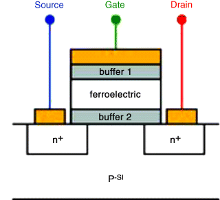
Figure 13.3 Typical ferroelectric FET structure. Reprinted with permission from Reference [54]
The FeFET is the only FET-based memory described in this chapter, and hence it has a slightly different performance and reliability characterization methodology than other (e.g., resistive switching) nonvolatile memories. The retention is typically based on either the time dependent difference in VT or difference in ID of the SET and RESET states of the after a given time period. The slope from these VT shifts following a few days to a few weeks are typically extrapolated to 10 years to provide a projected VT window after this time.
Prior to around 2004, progress on developing a scaled FeFET with reasonable retention was relatively slow [57]. In 2004, a 10 μm device was demonstrated with 1012 cycles of endurance which retained data for 12 days, maintaining an ION/IOFF ratio of 106 (although no long term endurance projection was made) [58]. In 2011, the first submicron FeFET with 10 year retention projected [59]. These devices utilized a Pt/SBT/Hf-Al-O/Si gate stack and had a minimum gate length 0.26 μm, and gave an endurance of 108 cycles. In this work, utilizing 20 μs writing pulses of −4 V and +6 V, an initial voltage window of 500 mV was obtained, and an estimated voltage window of ∼250 mV is extracted from a one week retention measurement [59]. In 2012, the same group demonstrated a 64 kbit FeFET array based on the Pt/SBT/Hf-Al-O/Si gate stack [60]. This array requires 10 μs ±7.5 V SET/RESET pulses, and achieves 108 cycle endurance. An initial window of 350 mV was demonstrated and a 10 year VT window of 200 mV was predicted (extrapolated from a 48 h measurement).
Recent demonstrations of ferroelectric silicon doped HfO2 (Si: HfO2) show some of best performance, reliability, and scaling data to date [53,61]. At IEDM 2011, HfSiO FeFETs were demonstrated which required 1 s programming with voltages of −3 V and +4 V and achieve an initial VT window of 1000 mV, which is predicted to be 650 mV after 10 years [53]. In 2012, a similar Si:HfO2 FeFET with a gate length of 28 nm was demonstrated, by integrating the ferroelectric HfO2 into the gate stack of a HKMG CMOS process [61]. This FeFET required 20 ns, ±5 V SET/RESET pulses and produced an initial VT window of 1000 mV. It was estimated that these devices would maintain a 600 mV window after 10 years (extrapolated from a 30 h measurement). Endurance on this highly scaled device was only 104 cycles due to significant charge injection.
Retention remains a key issue for the FeFET. All 10 year retention extrapolations are made from actual measurement lasting 12 days or less. Poor retention is due to two issues inherent in integrating a ferroelectric capacitor in a MOSFET gate stack: (a) the depolarization field and (b) charge trapping at the ferroelectric buffer- or ferroelectric-semiconductor interface [57]. The depolarization field occurs as a consequence of integrating a ferroelectric capacitor with a semiconductor. It is not possible for the ferroelectric to have the polarization charge compensated charge on the semiconductor side (even with a buffer layer) due to the capacitance of the semiconductor. The second issue, charge trapping at the interface of the ferroelectric and semiconductor, is caused by the remnant polarization field acting on this interface [53,57]. This charge eventually compensates the field created by the remnant polarization of the ferroelectric and effectively cancels the threshold voltage shift. Charge injection appears to be especially deleterious on highly scaled devices [61].
The FeFET is also difficult to integrate with CMOS, especially versions which rely on SBT or PZT. Doped HfO2 offers an improved method of CMOS integration, but additional research is still needed to understand the origins of ferroelectricity in this material. In addition, the FeFET always requires an FET structure, and hence is not easy to integrate as a back end of line (BEOL) memory, as with metal/insulator/metal structures like ReRAM and the ferroelectric tunnel junction. However, if the extremely high endurance of the FeFET could be combined with high speed, low energy switching, it could serve as a strong M-class SCM or DRAM replacement candidate.
13.4.2 Ferroelectric Tunnel Junction
The ferroelectric tunnel junction (FTJ), also referred to as ferroelectric polarization reversal memory, is an asymmetric, metal/insulator/metal or metal/insulator/semiconductor resistive switching memory device. The insulator is a thin ferroelectric film which causes the resistance measured through the electrodes vary significantly based on the polarization direction due to the giant tunnel electroresistance (TER) effect. The theoretical concept of giant TER was first proposed as a polar switch by Leo Esaki in 1971, although experimental demonstration was not achieved until the early twenty first century [62]. Typical ferroelectric insulators are perovskites, such as BaTiO3 (BTO) and Pb(Zr,Ti)O3 (PZT). One electrode is often a metal such as Pt or Au. The other (e.g., bottom) electrode is typically a conducting perovskite, such as LaxSryMnO [63] or SrRuO3 [64]. Recently, improved tunnel electroresistance was found by using a semiconducting bottom electrode, Nb:SrTiO3 [65].
The SET, RESET, and read procedures are similar to bipolar ReRAM, but the physical mechanism is markedly different. The resistance switching in an FTJ can be explained with the aid of Figure 13.4. The device is set to a low resistance state (LRS) by applying a positive voltage pulse to the top electrode (2–5 V, and 10 ns to 100 μs are typical experimental values) [63,65]. This voltage pulse causes the electric field in the ferroelectric layer to polarize in the direction of the bottom to top electrode, as illustrated in Figure 13.4a. In this state, the electron tunnel barrier, ϕ, is low compared to the opposite polarization (the average barrier for the LRS is denoted ϕ0 in Figure 13.4). A negative voltage pulse of roughly equal time and magnitude causes a reversal of the polarization, and the barrier rises to an average height of ϕL. The cell is read by measuring the current at a voltage low enough to avoid disturbing the polarization, typically on the order of 100 mV.
Figure 13.4 Physical depiction of a FTJ band diagram and device structure in: (a) low resistance (ON) state and (b) high resistance (OFF) state. The red arrows represent (a) high and (b) low current flow through the resistive element, based on the polarization direction, which influences the barrier height. Reprinted by permission from Macmillan Publishers Ltd: Nature, reference [66], copyright 2012
FTJ memory was realized for the first time in the past several years, and hence only a handful of proof of concept studies of memory cell characteristics have been performed. In 2012, a 50 nm FTJ memory was demonstrated [63], with an estimated potential to scale to 10 nm, based on the ferroelectric domain size [5]. This device had the very low write energy of 10 fJ/bit. The highest published endurance and retention values are given in Reference [67] for a Co/BiFeO3/Ca0.96Ce0.04MnO3 FTJ of 4 × 10⁶ cycles and 10 years, respectively. Reference [65] elucidates a common, but important tradeoff between retention, endurance, and write voltage can be found. If a write voltage of 3.5 V is used, ROFF/RON values of 104 are possible (which will increase retention), but endurance is limited to tens of cycles. In the opposite extreme, if a write voltage of 2.2 V is used the ROFF/RON drops to about 40, which increases the endurance but reduces the retention times and decreases read margins in an array.
FTJ memory shows promise as a scalable, ultra-low switching energy technology, but is relatively new and has many research challenges that must be overcome before being considered as a viable NAND flash, SCM, or DRAM replacement candidate. One of the key research areas is to prove that a single FTJ can have an endurance greater than 106, while maintaining reasonable retention. Scaling down to 10 nm or less must also be proven. Furthermore, it will be technologically important to develop an FTJ using CMOS compatible materials; one possibility is to take advantage of ferroelectricity discovered recently in doped HfO [52]. Another important step will be to develop FTJ memory arrays and explore the cell to cell variation and yields.
13.5 Mott Memory
Mott memory is a resistive switching memory cell with a similar structure to metal oxide ReRAM, sometimes referred to in the literature as a correlated electron RAM (CeRAM) [68]. Specifically, this is a metal/insulator/metal structure utilizing a Mott insulator. Common Mott insulators used in memories are VOx, Pr1−xCaxMnO3, and NbOx. In these materials, the standard quantum theory of solids, such as the tight-binding model, predict that these materials should act as electrical conductors [69]. The standard tight-binding model uses the independent electron approximation, which does not account for strong electron-electron interactions, where a short screening length exists. In a Mott insulator, the high electron density under certain conditions creates a short enough electron screening length that electrons interact with each other such to create an energy gap and impede conduction. One can consider the simple physical picture: these extremely high densities of electrons strongly repulse each other and resist conduction. A Mott insulator transitions to metallic behavior past a particular material dependent temperature, known as the metal insulator transition (MIT) transition temperature. For example, this has been shown to occur at ∼1070 K in NbO2 [70].
Switching in a Mott insulator typically occurs due to a metal insulator transition induced by current injection in the device, and can be unipolar [71] or bipolar [68,72]. In fact, the electrical switching of a Mott memory shares similarities with oxide-based ReRAM (hence in some cases the Mott transition is considered an alternate explanation to ionic motion for resistance switching in certain metal oxides [71,72]). In a Mott memory, a voltage pulse forces the Mott transition (which naturally occurs at the MIT temperature). A voltage pulse of either opposite polarity [72], or different waveform [72] causes the device to return to its conducting state. The ability to use a current to cause a Mott insulator to reach the insulating state is expected, and accounts for the behavior of Mott oscillators [73].
Mott switching has the advantages of high speed and low energy. For example, switching at speeds below 3 ns, and endurance of 109 cycles, with energies around 100 fJ in NbO crossbar devices have been demonstrated [72]. However, these devices were not nonvolatile (nor were they intended to be – these were being explored as a resistive memory select device), and lost their state as soon as they cooled, typically in a few ns. Carbonyl doped NiO Mott memories with an endurance of 100 cycles were reported to retain data for 1 h at 300 °C [68].
Theoretical understanding and experimental demonstration of retention in Mott memory is an important research challenge. In devices that exhibit retention of conduction below MIT temperature, it will be necessary to demonstrate high endurance, scaling, and eventually functional arrays. If long retention cannot be demonstrated, it is also possible that Mott insulators can be used as a select device for resistive memory arrays [73] (see Chapter 12).
13.6 Macromolecular Memory
The category of macromolecular memory, also referred to as polymer, or organic memory, encompasses a wide variety of memory devices [74,75] (also see Chapter 10). The defining feature of this category is the incorporation of polymers in the switching layer. For brevity the following treatment focuses on the category of devices which exhibit resistance change due to this polymer layer. This category of macromolecular memory has demonstrated the best performance metrics [5]. A very thorough description of other types of polymer memories, including capacitor and FET structures is given in reference [74].
The resistive macromolecular memory structure consists of a metal/insulator/metal structure, where the insulating/switching layer is a polymer – which is often organic. There are numerous resistance switching mechanisms reported in macromolecular memories, which are not yet fully understood. The read and write operations in a resistive macromolecular memory are similar to those in ReRAM and it is possible define a similar set of categorization to the ReRAM scheme presented above. Bipolar voltage induced electrochemical formation and dissolution of an Ag filament was directly observed in an Ag/WPF-BT-FEO3/Conducting-Si stack [76]. This is a strong indication that the mechanism is analogous to the electrochemical metallization bridge (EMB) ReRAM described in Section 13.3.1, except that the insulating layer has been replaced by an organic polymer. Anionic motion, similar to the unipolar and bipolar metal oxide ReRAM has been proposed as another switching mechanisms in several macromolecular memory devices [74]. A mechanism for bipolar switching reported by several groups is the creation and annihilation of a charge transfer (CT) complex due to an electric field [75,77,78]. This mechanism is unique to polymer memories. When formed, a charge transfer complex allows the flow of charge through the normally insulating polymer.
A number of promising macromolecular memory devices have been recently been reported. A 2 × 2 μm Al/parylene-C/parylene-C/W cell has been demonstrated to exhibit bilayer switching with a RESET current of 18 nA (a 150 nA SET current is required) at a power of 67 nW [79]. Assuming that the RESET switching is 15 ns, as reported for an earlier parylene-C memory [80], a switching energy of 1 fJ is possible. This device exhibited a retention of ∼104 s (∼3 h) at 200 °C and endurance of about 100 cycles [79]. The highest reported endurance in a macromolecular memory comes from an Al/polymide/ITO cell, using a polymide named “DAXIN-PI” [78]. This bipolar device exhibited 105 SET/RESET cycles (using 200 ns ±2 V pulses) and with retention of ∼3 h at 85 °C, following this endurance test. SET and RESET voltages were as low as 1.0 and −0.3 V, respectively, and a maximum ROFF/RON ratio of 105 was demonstrated. As with other types of ReRAM, tradeoffs between switching voltage, switching time, endurance, and retention exist. A relatively long retention time4 of over 106 (>32 days) was obtained by using a Al/PEDOT:PSS5/Cu bipolar electrochemical metallization type cell [81].
A highly scaled 8 × 8 crossbar array of 100 nm Al/PI:PCBM/Au with unipolar resistive switching cells has been demonstrated [82]. For macromolecular memories which rely on filamentary conduction, it is reasonable to assume that the ultimate scaling limits will follow that of EMB, or MO-BF type ReRAM due to small filament sizes. For example, in Reference [81], the size of the Cu filament is calculated to be about 4.1 nm (from resistivity calculations).
The 8 × 8 array work presented in reference [82] also provided baseline statistics for the 64 cells (statistical analysis was done for the array with 2 × 2 μm2 devices). The yield was 50 out of the 64 cell array (∼78%). Both the high resistance state had a spread of about two orders of magnitude, and the average ROFF/RON was about 105, so the distributions did not overlap. A stacked three layer set of 8 × 8 crossbars of unipolar 200 × 200 μm PI:PCBM-based cells, stacked between Al metal lines has been demonstrated [83]. In this case, the yield was 160/192 bits (83%). High resistance state values had a relatively large spread (about four orders of magnitude), but still did not overlap with the low resistance states. Large variation in the high resistance state of cells is a common attribute of metal oxide ReRAM [11]. Similar PI:PCBM 8 × 8 arrays have also been demonstrated on a flexible substrate with relatively similar performance [84], demonstrating the possibility of use as a NVM for flexible electronics.
Macromolecular memories are interesting from the fundamental material science perspective, and present interesting prospect as a future memory technology. However, several key challenges must be addressed to make macromolecular memory viable as a mainstream commercial product. An important, fundamental challenge of macromolecular memories is, as with ReRAM, to obtain an improved understanding and categorization of macromolecular resistive switching mechanisms [75]. At the cell level, endurance and retention in most reports are low (<200 cycles endurance and <3 h retention are typical [79,80,82]). Demonstration of proof of concept devices that combine low energy, high endurance, high retention, and excellent scalability in a single device is a key milestone. Furthermore, most polymers used in these memories are not considered CMOS compatible materials, and it is not clear that these memories will survive integration with a typical CMOS at typical BEOL temperatures.
13.7 Carbon-based Resistive Switching Memory
Restive switching in numerous forms of carbon has been reported in recent years. A straightforward method to categorize these emerging memory technologies is by the form of carbon that facilitates switching: carbon nanotubes, amorphous carbon (a-C), diamond-like carbon (DLC), graphene, and graphene oxide. The physical switching mechanisms reported vary widely, which include the change from the sp2 to sp3 state in carbon [85], redox mechanisms (as described above in Section 13.4 and in Chapter 8), charge trapping (described in Chapter 9), and nanoelectromechanical switching. In addition to reports of resistive switching in the carbon material, carbon nanotubes have been utilized as electrode materials for other types of memory including phase change [86] and metal oxide–bipolar filamentary ReRAM [39]. In the following, we briefly survey the state of the art of carbon-based resistive switching memories.
13.7.1 Amorphous Carbon and Diamond-like Carbon
An amorphous carbon (a-C) or diamond-like carbon (DLC)-based resistive switch consists of an electrode/x/electrode structure similar to other ReRAM cells, where x is an a-C or DLC layer. Resistive switching in amorphous carbon is reported to result from numerous different physical mechanisms. In several reports, unipolar switching in a-C [85,87] and DLC [88] is thought to occur due to the formation and rupture of a sp3 filament in the material. This case is analogous to metal oxide-unipolar filamentary ReRAM, as the SET and RESET mechanism are both thermochemical.
In another case, when the structure includes a Cu or Ag electrode, and bipolar switching occurs, it is reasonable to propose that the electrochemical formation and dissolution of a metal filament cause switching. This has been observed in both Cu/a-C/electrode and Ag/a-C/electrode structures [89]. In this case, the memory is an EMB ReRAM cell (as discussed above), where the insulating layer is composed of amorphous carbon rather than the more traditional EMB materials such as chalcogenides and metal oxides.
13.7.2 Graphene and Graphene Oxide
Graphene-based memories have been reported by multiple groups [90–93]. A resistive switching structure is typically comprised of a graphene strip contacted on both sides by electrodes (i.e., Pt [90] or Cr/Au [92]). One proposed mechanism of switching in graphene is the nanoelectromechanical breaking and reattaching of the strip [90]. Bipolar resistive switching in a graphene strip has also been explained by charging effects [90].
Bipolar switching has also been reported in metal/graphene oxide (GO)/metal structures. In the case where one of the electrodes is Cu, it is likely an electrochemical metallization bridging effect occurs, similar to the EMB ReRAM. A Cu/GO/Pt structure with bipolar switching at ∼1 V, with a ROFF/RON ratio of 20 and retention of 104 s has also been reported [90]. A flexible Al/GO/Al structure was demonstrated with bipolar switching at about 3.5 V, suggesting a valence change mechanism similar to that in MO-BF ReRAM.
13.7.3 Carbon Nanotubes
Carbon nanotube memory originally attracted significant attention in the year 2000, after the concept of a highly scaled memory array with each cell was defined by the cross-section of two carbon nanotubes was presented [94]. The proposed mechanism for switching in such an array was the electrostatic repulsion and attraction of the two crossing nanotubes. More recently, a full prototype memory chip IC was demonstrated based on lithographically defined carbon nanotube resistance switching layers [95]. The proposed switching mechanism is fundamentally the same electrostatic resistance switching mechanism reported in reference [94]. However, it was hypothesized in the lithographically defined nanotube layers that the connection and repulsion of many nanotubes in concert is responsible for the observed resistance change [95]. The 4 Mb test chip based on 22 nm carbon nanotube layer memory cells has a typical SET operation requiring a 5 V pulse for 500 ns, with a typical current of 1 μA. The RESET operation requires a 50 ns, 4.5 V pulse resulting in a typical current of 15 μA. Assuming both currents give are averages, the SET and RESET switching energies are 2.5 pJ and 3.4 pJ respectively. An endurance of 104 cycles and retention of 24 h at 125 °C are reported for this prototype. For this carbon nanotube layer-based NVM technology, few fundamental studies have been published, and hence it is difficult to verify the switching mechanism.
13.7.4 Research Challenges
Carbon memories present interesting features, such as high temperature operation, flexible arrays, and simple processes. However, carbon memory is a relatively young field with many research challenges. Foremost is the understanding of switching mechanisms in different materials. Resistive switching in amorphous carbon and graphene oxide appear to have similarities to redox memory; if this is verified it would be appropriate to consider them a member of the ReRAM family. More fundamental work is needed to understand and verify the proposed switching mechanisms in each category of emerging carbon memory.
13.8 Molecular Memory
Molecular memory is a resistive switching structure based on a single monolayer of molecules surrounded by electrode materials. The memory effect is related to the change in the charge state of a molecule such that conductivity is modulated. Molecular memory is intriguing from the scientific perspective, and offers the possibility of very high scalability and low energy.
One of the earliest demonstrations of molecular memory was made from self-assembled monolayers of four different benzene-based molecules between Au electrodes [96]. This memory was bipolar, requiring a +5 V SET and −5 V RESET process. The retention in this demonstration was only ∼15 min, which would categorize it as a volatile memory. Another significant effort focused on bipolar switching of a [2]rotaxane-based molecular switch tunnel junction (MSTJ) in crossbar configurations [97,98]. In 2007, a rotaxane-based 160 kb molecular memory array was demonstrated [99]. Switching was achieved with 200 ms pulses of +0.2 (SET) and −1.5 V (RESET). This array had a yield of about 25%, with an average retention of about 90 min and maximum retention of about 180 min.
Molecular memory has many challenges, and research activity has declined in recent years.6 A major research topic related to molecular memory continues to be separation of the effects of the contacts from the molecular switching. Other key research challenges include very short retention times, low endurance, high variation, and low yield.
Recently, novel work using DNA as a storage medium was presented which offers an alternative promising molecular method of extremely dense information storage [100,101]. Arguably, the DNA molecule demonstrates storage density several orders of magnitude higher than other known storage technologies. The storage density of molecular DNA memory is ∼1019 bit/cm3, and 1 kg of DNA could store a maximum theoretical capacity of ∼2 × 10¹⁸ Mbit, which exceeds the world's current total information storage capacity [102]. Recent progress in DNA synthesis and sequencing has made it possible to experimentally explore DNA storage beyond biological applications. A major breakthrough occurred in 2012–2013 when mainstream digital formats were demonstrated to be compatible with DNA storage, offering a 1000× improvement in density [100,101]. DNA volumetric memory density far exceeds (1000×) projected ultimate electronic memory densities [103]. Also, in the living cell, the memory read/write operations occur at high speed (<100 μs/bit) and require very low energy (∼10−11 W/GB) [103].
There are still many unknowns regarding both DNA operations in cells and with regard to the potential of DNA technology for massive storage applications. One of the research goals is to demonstrate miniaturized, on-chip integrated DNA storage. New technologies for DNA synthesis and sequencing described above are key components of this work. For example, there are recent promising demonstrations of micro-manufactured DNA devices, such as a “DNA transistor” for sequencing [104]. Based on the rapid and continuing progress in DNA technologies, it is reasonable to suggest that research toward the integration of DNA memory systems with semiconductor integrated circuits could provide an impetus for highly dense memory systems operating at very low power.
13.9 Assessment and Benchmarking
Key concepts, recent status, and challenges of 10 emerging memory device technologies have been presented. It is useful to compare and contrast the applicability of these technologies against the required benchmark of their prospective markets. Estimated quantitative and qualitative requirements for key markets are provided in Table 13.1. This table is populated from the 2013 ITRS ERD and PIDS chapters, as well as external sources where noted. The quantitative data provided are estimates, and can vary greatly depending on the specific implementation of the memory. For example, DRAM used in a supercomputer may have considerably higher performance requirements than that used in a mobile device, such as a tablet. The data presented is intended as a useful starting point against which emerging memory technologies can be benchmarked. It should also be noted that switching energy and read/write latency requirements are given at the system level. Numbers for emerging memories are typically given for the device or array level. Hence, system architecture and circuit-level considerations may determine switching energy and latency rather than performance of the memory itself. System versus device level energetics are discussed further for DRAM and flash memory in Chapter 3.
Table 13.1 Approximate requirements for emerging memories categorized by available markets
| Embedded EEPROM replacementa | NAND flash replacement (e.g., SSD)b | S-type storage class memoryc | M-type storage class memoryc | Stand-alone DRAM (DIMM) replacementd | CMOS integrated DRAM/storage/main memorye | |
| Time to implementation | Now | 2–5 yr | 2–5 yr | 5–10 yr | 5–10 yr | >10 yr |
| Quantitative requirements | ||||||
| Minimum bit level endurance | 106 | 103 | 106 | 109 | 1016 | 1016 |
| Minimum bit level retention | 10 yr | 1 yr | 10 yr | 5 d | 64 ms | 10 yr |
| Maximum system level read/write latency | 100 μs | 100 μs | 5 μs | 200 ns | 100 ns | 10 ns |
| Maximum system level write energy (pJ) | 104 | 100 | 25 | 100 | 100 | 1 |
| Maximum feature size (nm) | 180 | 12 | 20 | 20 | 20 | 10 |
| Minimum 2D layer density (bit/cm) | 109 | 1011 | 1010 | 1010 | 109 | 1011 |
| Maximum cost (US$/GB) | 30f | 2 | 4 | 10 | 10 | 10 |
| Qualitative requirements | ||||||
| Performance | Low | Low | Moderate | High | High | High |
| Reliability | High | Low/moderate | Moderate | Moderate | Moderate | High |
| CMOS compatibility | Required | Useful/not required | Useful/not required | Useful/not required | Useful/not required | Required |
| BEOL process | Required | Not required | Not required | Not required | Not required | Required |
| Layering capability | Not required | Required | Required | Useful/not required | Required | Required |
| aBased on common embedded microcontrollers with flash-based program/data memory. | ||||||
| bBased on modern NAND flash characteristics, considering a stand-alone module. | ||||||
| cBased on SCM info from 2013 ITRS ERD Tables. | ||||||
| dBased on modern DRAM characteristics. | ||||||
| eHigh performance logic CMOS integration based on estimated requirements for data-center level processor (e.g., a “nanostore” [6]). This could also be thought of as a “univeral memory” which does not require tradeoffs in performance or reliability. | ||||||
| fBased on the cost of a standalone external microcontroller memory; information on the cost per bit of flash integrated in a microcontroller is not available. | ||||||
Table 13.1 is arranged in order of the approximate time emerging memory technologies would likely enter the market. Embedded EEPROM replacement involves the replacement of an EEPROM cell in an embedded microcontroller or field programmable gate array (FPGA). An example of this is provided in Reference [7], which describes a microcontroller product with a monolithically integrated ReRAM memory. As indicated by the requirements, the EEPROM market has the lowest barrier to entry and is a good niche starting point for emerging memories. Flash memory is currently a ∼US$ 30 billion/year market, the majority of which is NAND. For this reason, displacing NAND flash will be an important near term goal of emerging memories. The most important attributes for this market are scaling to higher densities and at a lower cost than NAND flash. Storage Class Memory is a market opportunity for emerging and prototypical memories, based on the large latency gap between typical magnetic- or flash-based disk drives and the DRAM main memory. SCM would replace magnetic memory, solid state disks (SSDs), and possibly even DRAM with one or more emerging memory technologies (NAND flash is considered a low-end or early SCM technology). M-Class SCM has performance and endurance characteristics closer to those of DRAM, whereas S-Class is reminiscent of flash, with lower performance, but a high retention requirement. DRAM serves as the main working memory for a wide variety of systems, including PC and most mobile devices, such as tablets and smartphones. It has effectively unlimited endurance and a low read/write latency, but retention of less than 1 s. The final market in Table 13.1 does not currently exist, but is a straw man for a memory integrated with high performance logic; similar to that suggested by the “Nanostore” concept [6]. In the following, we assess quantitative characteristics of emerging technology, with regard to the requirements of these potential markets.
Tables 13.2 and 13.3 provide a compilation of quantitative performance parameters for emerging memory technologies, including best projected and demonstrated values of key metrics with references as given. The values are from the 2013 ITRS ERD tables and references therein [5].
Table 13.2 Parameters for emerging memory technologies (excluding ReRAM). Numbers are from the 2013 ITRS ERD Table 4a and references therein [5]. Research activity is given in number of peer reviewed publications indexed from July 2011 through July 2013
| Emerging ferroelectric memory | Carbon memory | Mott memory | Macromolecular memory | Molecular memory | |||
| Subclass | FeFET | FE tunnel junction | NA | NA | NA | NA | |
| Feature size F (nm) | Best projected | Same as CMOS transistor | <10 | <5 | 5–10 | 5 | 5 |
| Demonstrated | 28 | 50 | 22 | 110 | 100 | 30 | |
| Cell area | Best projected | 4F2 | 4F2 | 4F2 | 4F2 | 4F2 | 4F2 |
| Demonstrated | 4F2 | Not available | Not available | Not available | 4F2 | Not available | |
| Write/erase time | Best projected | <100 pS | <1 ns | Not available | <1 ns | <10 ns | <40 ns |
| Demonstrated | 20 ns, 10 ns | 10 ns | 10 ns | 2 ns | 15 ns | 10 s, 0.2 s | |
| Retention time | Best projected | 10 yr | >10 y | Not available | Not available | > 1 yr | Not available |
| Demonstrated | 2.5 × 10⁵ s (3 d) | 3 d | 168 h at 250 °C | Not available | 105 s | 2 mo | |
| Write cycles | Best projected | >1012 | 1014 | Not available | >1016 | Not available | >1016 |
| Demonstrated | 1012 | 4 × 10⁶ | 5 × 10⁷ | ∼100 | 105 | 2 × 10³ | |
| Write operating voltage (V) | Best projected | Not available | 1 | Not available | Not available | ∼1 | 80 mV |
| Demonstrated | ±5 | 2–3 | 5–6 | 1.25/0.75 | 1.4 | 4.0 ± ∼1.5 | |
| Read operating voltage (V) | Best projected | Not available | 0.1 V | Not available | Not available | <0.1 | 0.3 |
| Demonstrated | 0.5 | 0.1 | 1.5 | 0.2 | 0.2 | 0.5 | |
| Write energy per bit | Best projected | 0.1 fJ | 1 fJ | Not available | Not available | 0.1 fJ | 0.1 aJ |
| Demonstrated | 1 fJ | 10 fJ | Not available | ∼1 fJ | 10 fJ | Not available | |
| Research activity | 30 | 27 | 52 | 31 | 80 | 21 |
Table 13.3 Parameters for the four categories of ReRAM [5]. Numbers are from the 2013 ITRS ERD Table 4b and references therein. Research activity is given in number of peer reviewed publications indexed from July 2011 through July 2013
| Electrochemical metallization bridge | Metal oxide: bipolar filamentary | Metal oxide: unipolar filamentary | Metal oxide: bipolar nonfilamentary | ||
| Storage mechanism | Electrochemical filament formation | Valence change filament formation | Thermochemical effect filament formation | Change in tunneling characteristics near interface | |
| Feature size F (nm) | Best projected | <5 | <5 | Not available | <10 |
| Demonstrated | 20 (GeSe), 30 (CuS) | 5 (AlOx) | 35 | 40 | |
| Cell area (2D) | Best projected | 4F2 | 4F2 | 4F2 | 4F2 |
| Demonstrated | 4F2 | 4F2 | 4F2 | 4F2 | |
| Write/erase time (ns) | Best projected | <1 | <1 | not available | 10 |
| Demonstrated | <1 | <1 | 10 (W), 5 (E) | <100 | |
| Retention time | Best projected (yr) | >10 | >10 | >10 | >10 |
| Demonstrated | 1000 h at 200 °C | 3000 h at 150 °C | 1000 h at 150 °C | 4 h at 125 °C | |
| Write cycles | Best projected | >1011 | >1012 | Not available | >106 |
| Demonstrated | 1010 | 1012 | 106 | 106 | |
| Write operating voltage (V) | Best projected | <0.5 | <1 | Not available | Not available |
| Demonstrated | 0.6 | 1–3 | 1–3 | 2 | |
| Read operating voltage (V) | Best projected | <0.2 | 0.1 | Not available | 0.1 |
| Demonstrated | 0.2 | 0.1–0.2 | 0.4 | 0.5 | |
| Write/erase energy (J/bit) | Best projected | Not available | 0.1 fJ | Not available | Not available |
| Demonstrated | 1 pJ (W), 8 pJ (E) | 115 fJ (W), <1 pJ (E) | Not available | 1 pJ | |
| Research activity | 593 (includes all categories) |
13.9.1 Scaling
The scalability of an emerging memory technology is a key factor for it to be considered a strong candidate to replace traditional data storage technologies. Although NAND flash has been scaled to a 2D density of 16 nm, a density of roughly 9 × 1010 bits/cm2 (or ∼11 GB/cm2), these ultra-scaled devices have suffered severely degraded retention, endurance, and yield [5]. DRAM also has “no known solutions” for scaling challenges below the 20 nm half pitch, occurring in 2017 [5]. The maximum density a memory technology can reach is defined by the minimum feature size F and cell area, in terms of F. The maximum density of a layer is plotted in Figure 13.5 for a given feature size using a cell area of 4, 6, and 8 F2.
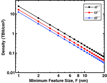
Figure 13.5 Density versus minimum feature size (F) for cell sizes of 4F2, 6F2, and 8F2
Scalability is one of the categories evaluated in both the qualitative and quantitative sections of the ERD chapter. Scalability below 10 nm is predicted for all emerging memories, although it has only been demonstrated for BF-MO ReRAM (see Table 13.3). This matches the qualitative opinion reflected in the expert survey that ReRAM has the highest potential scalability (Table 13.4). It is reasonable to conclude that other emerging memories that rely on filamentary switching, such as certain types of carbon and macromolecular memory, will scale to the same dimensions as standard filamentary ReRAM. The high scalability of ReRAM makes it especially attractive as a NAND flash replacement for S-type SCM technology.
Table 13.4 Qualitative assessment of emerging memory technologies sorted by overall score. Based on the expert survey presented in the 2013 ITRS ERD chapter [5]
| Overall | Scalability | Speed | Energy efficiency | ON/OFF “1”/“0” ratio | Operational reliability | Room temperature operation | CMOS technological compatibility | CMOS architectural compatibility | |
| ReRAM | 18.7 | 2.9 | 2.5 | 2.1 | 2.2 | 1.6 | 2.5 | 2.4 | 2.4 |
| FeFET | 17.4 | 2.0 | 2.4 | 2.3 | 2.1 | 1.7 | 2.4 | 2.3 | 2.4 |
| FTJ | 17.3 | 2.3 | 2.2 | 2.2 | 2.1 | 1.7 | 2.4 | 2.1 | 2.2 |
| Carbon-based | 17.0 | 2.2 | 2.2 | 2.0 | 2.3 | 1.7 | 2.4 | 2.0 | 2.2 |
| Mott | 16.6 | 2.1 | 2.4 | 2.1 | 2.2 | 1.7 | 1.9 | 2.0 | 2.2 |
| Macromolecular | 13.9 | 1.8 | 1.7 | 1.7 | 1.6 | 1.3 | 2.2 | 1.7 | 1.8 |
| Molecular | 13.9 | 2.6 | 1.7 | 2.0 | 1.3 | 1.1 | 2.0 | 1.6 | 1.8 |
In certain memory categories listed in Table 13.1, such as M-type SCM and DRAM replacement, scaling is less important than performance factors, such as endurance, write speed, and energy. For example, while it is possible that the FeFET may not scale as well as ReRAM, but the high endurance may still make it a strong DRAM replacement candidate.
13.9.2 Performance
Emerging memory performance is assessed quantitatively in Tables 13.2 and 13.3 by write/erase speed, energy, and voltage. Performance is assessed qualitatively from survey results in Table 13.4, as an assessment of speed, energy efficiency, and ON/OFF ratio. Demonstrated SET/RESET speeds are 20 ns or less for all technologies except molecular memory and MO-BN ReRAM. Where available, all technologies had demonstrated switching energies of less than 10 pJ, and in many cases less than 1 pJ. Interestingly, the qualitative assessments of speed and energy efficiency are lowest for macromolecular memory, even though there are very competitive values reported in the literature for this technology. Differences in performance records reported in the literature and the opinion conveyed by the survey of experts might reflect significant recent improvement in performance, or the anticipation of difficulty achieving record performances on production devices. As described in Chapter 3, array and architectural considerations will ultimately determine the system level speed and energy requirements of each of these memories. For example, a DRAM cell only requires about 10 fJ at the cell level but at the system level requires ∼50 pJ.
13.9.3 Reliability
Write cycles (endurance) and retention data are the main quantitative measures of reliability provided in Tables 13.2 and 13.3, although other factors, such as device to device variability and random telegraph noise (RTN) are also important reliability considerations in memory device reliability. Variability and RTN are somewhat difficult to assess in a quantitative comparison table, but are expected to influence the expert survey opinions of “operational reliability” provided in Table 13.4.
The minimum endurance required for an emerging memory to enter any of the application markets described in Table 13.1 is about 106 SET/RESET cycles. This endurance has been demonstrated in all categories of ReRAM, ferroelectric, and carbon memory (except graphene memories). If a memory technology has an endurance of less than 106, it is likely that workarounds such as error correction code (ECC) and garbage collection routines will be needed (as with modern NAND-flash memory). Mott, molecular, and macromolecular memory have not yet met this requirement (although macromolecular has achieved 105 cycles), and hence achieving this endurance should be a key research in those technologies.
For M-type SCM and DRAM replacement applications, higher endurance is required. M-type SCM requires one billion cycles, whereas straightforward DRAM replacement would require 1016 SET/RESET cycles. The requirement of a billion cycles has been met by the FeFET, as well as EMB and MO-BF ReRAM. This high endurance, along with excellent performance makes these technologies potential M-type SCM and DRAM replacements. In the case of the FeFET, the low retention is not an impediment for these technologies.
The retention required for the traditional NVM applications of embedded EEPROM and NAND-flash, as well as S-type SCM is 10 years (typically retaining data at a temperature of 85 °C). Since it is difficult to make a measurement over 10 years, retention is typically projected from accelerated measurements [41], but there is not a standardized method of reporting these projections in an emerging memory device [105]. ReRAM (except for non-filamentary) are projected to meet this 10 year requirement from relatively detailed retention studies that derived from thorough arhennius studies. Ten year retention is also predicted for the FeFET and FTJ, although the longest demonstrated periods are about three days for each, and hence additional data is needed to verify this claim. For a DRAM replacement and M-type SCM memory retention is much less important (whereas endurance is key), and hence the FeFET and FTJ are still a strong contenders.
Qualitatively, all emerging memories scored low in the “operational reliability” category. This can be presumably attributed to several factors, especially variability in the SET and RESET states between devices and lack of long term reliability data. This illustrates the general fact that after basic functionality of an emerging memory technology is demonstrated, research and development efforts must prove reliability before being accepted in any of the markets listed in Table 13.1. Perhaps finding a niche, low consequence market which allows the memory product to demonstrate reliable operation of high quantities of parts is the best approach to gain widespread use of an emerging memory technology [11].
The scores for macromolecular and molecular memories were the lowest at 1.3 and 1.1, respectively. This indicates a strong need for these technologies to focus research efforts on proving that reliable operation is possible, otherwise commercial adaptation of these technologies is unlikely.
13.9.4 CMOS Compatibility and Cost
CMOS compatibility and cost are, perhaps, the most subjective requirements for emerging memory technology, although they are also often the greatest factors which determine commercial success in any market. All emerging memories discussed except for the FeFET employ back end of line (BEOL) processing, and hence their CMOS compatibility should be assessed with regard to BEOL materials and temperatures. ReRAM received the highest score on CMOS compatibility, which likely reflects that at least for certain ReRAM devices, there are no special materials required and that this technology can survive typical BEOL CMOS temperatures (which are typically a maximum of 400 °C). The lowest scores were given to macromolecular and molecular memories, and can be attributed to two problems. First, both of these technologies require special materials not typically found in fabrication, (such as polymers). Second, it is not clear that many of these polymers or molecules can survive BEOL temperatures and process conditions.
Another important factor in CMOS compatibility is the maximum voltage require in the SET or RESET operation. EMB ReRAM has the lowest demonstrated switching voltages (0.6 V has been demonstrated), which provides an advantage in the integration with advanced CMOS nodes without the need for a separate high voltage transistor.
13.9.5 Tradeoffs
One of the greatest shortcomings of Tables 13.2 and 13.3 is that they present record performance and reliability metrics for different devices of a particular technology column. For example, in the MO-BF ReRAM different devices were used to demonstrate scaling to 5 × 5 nm, sub-ns switching, 1012 cycle endurance, and 10 year retention at >100 °C. A single device with all of these characteristics has not been demonstrated. It should also be noted that these parameters come from array demonstrations when possible, but are often from single devices. More mature technologies like EMB ReRAM have metrics taken from sophisticated test chips which closely resemble future commercial products, whereas the least developed technologies generally have parameters available at the research device level. As discussed in Chapter 3, array parasitics and peripheral circuitry can significantly increase the write energy. Power considerations of passive resistive memory arrays have been modeled in reference [106]; and array level energetics of these arrays is an important area of future work.
Hence, it may not be possible to obtain a device or an array in a given emerging memory technology that has all of the characteristics of a column in Tables 13.2 and 13.3. This methodology is intended only to provide the most optimistic characteristics of emerging memory technology with a single data set.
It is therefore worthwhile to consider the tradeoffs that prevent the simultaneous achievement of every parameter for a column of Tables 13.2 or 13.3. One common example of this type of tradeoff is that between switching current (which is reflected in switching energy) and retention of a ReRAM cell. An example of this is provided in Reference [40], whereas the compliance current used during switching is the key factor which determines retention. When the compliance current of 100 μA is used to SET the device, a wider, more robust filament is formed compared to when 10 μA is used. Hence, the temperature at which 10 year retention is possible is 105 °C for a 100 μA cc but only 95 °C for a 10 μA cc. This demonstrates that it is possible to increase the retention of a ReRAM cell if one is willing to pay the price in switching current (and therefore switching power). Fundamental energy–space–time tradeoffs for ReRAM are discussed in detail in Reference [107].
13.10 Summary and Conclusions
Several emerging memory devices provide promising features to compete with dominant conventional memory technologies: floating gate (NAND/NOR flash and embedded EEPROM), and DRAM. They also may enable system improvements by serving as M- and S-type Storage Class Memory technologies. ReRAM has made especially rapid progress in the past two years, and may be nearing commercial viability for niche markets. Interest in FeFET and FTJ has been reinvigorated by the discovery of ferroelectricity in doped HfOx, which may enable a surge of progress for emerging ferroelectric memories.
Reliability remains a key challenge for all emerging memory technologies – and should be a major focus of future research efforts. Although several emerging memory technologies have demonstrated excellent performance characteristics, they will not become commercially viable until reliable system-level operation in native environments is unquestionably established.
Acknowledgments
The authors would like to acknowledge R.J. Kaplar and P.R. Mickel (Sandia) and A. Chen (Globalfoundries), and J. Hutchby (SRC) for reviewing and making useful comments on this manuscript. One author (M.J.M.) would like to acknowledge funding from Sandia's Laboratory Directed Research and Development (LDRD) Program. Sandia National Laboratories is a multi-program laboratory managed and operated by Sandia Corporation, a wholly owned subsidiary of Lockheed Martin Corporation, for the US Department of Energy's National Nuclear Security Administration under contract DE-AC04-94AL85000.
Notes
References
- 1. Micron (2013) Micron Unveils 16-Nanometer Flash Memory Technology. Available: investor.micron.com/releasedetail.cfm?ReleaseID=777402 (accessed 16 July 2013).
- 2. Samsung (2013) Samsung Starts Mass Producing Industry's First 3D Vertical NAND Flash. Available: http://www.samsung.com/global/business/semiconductor/news-events/press-releases/detail?newsId=12990 (accessed 16 July 2013).
- 3. Freitas, R.F. and Wilcke, W.W. (2008) Storage-class memory: The next storage system technology. IBM Journal of Research and Development, 52, 439–447.
- 4. Burr, G.W., Kurdi, B.N., Scott, J.C. et al. (2008) Overview of candidate device technologies for storage-class memory. IBM Journal of Research and Development, 52, 449–464.
- 5. (2013) The International Technology Roadmap for Semiconductors (ITRS). Available: www.itrs.net.
- 6. Ranganathan, P. (2011) From microprocessors to nanostores: Rethinking data-centric systems. Computer, 44, 39–48.
- 7. Panasonic (2013) Panasonic Starts World's First Mass Production of ReRAM Mounted Microcomputers. Available: http://panasonic.co.jp/corp/news/official.data/data.dir/2013/07/en130730-2/en130730-2.html (accessed 16 July 2013).
- 8. Adesto (2013) Available: www.adesto.com (accessed 16 September 2013).
- 9. Tz-Yi, L., Tian Hong, Y., Scheuerlein, R. et al. (2013) A 130.7 mm2 2-layer 32Gb ReRAM memory device in 24nm technology. ISSCC Dig. of Tech. Papers, pp. 210–211.
- 10. Chevallier, C.J., Chang Hua, S., Lim, S.F. et al. (2010) A 0.13 um 64 Mb multi-layered conductive metal-oxide memory. ISSCC Dig. of Tech. Papers, pp. 260–261.
- 11. Prall, K., Ramaswamy, N., Kinney, W. et al. (2012) An Update on Emerging Memory: Progress to 2X nm. 4th IEEE International Memory Workshop, pp. 1–5.
- 12. Waser, R., Dittmann, R., Staikov, G., and Szot, K. (2009) Redox-based resistive switching memories – nanoionic mechanisms, prospects, and challenges. Advanced Materials, 21, 2632–2663.
- 13. Valov, I. and Kozicki, M.N. (2013) Cation-based resistance change memory. Journal of Physics D-Applied Physics, 46, 074005.
- 14. Valov, I., Waser, R., Jameson, J.R., and Kozicki, M.N. (2011) Electrochemical metallization memories—fundamentals, applications, prospects. Nanotechnology, 22, 254003.
- 15. Kozicki, M.N., Dandamudi, P., Barnaby, H.J., and Gonzalez-Velo, Y. (2013) (Invited) programmable metallization cells in memory and switching applications. ECS Transactions, 58, 47–52.
- 16. Goux, L., Sankaran, K., Kar, G. et al. (2012) Field-driven ultrafast sub-ns programming in W/Al2O3/Ti/CuTe-based 1T1R CBRAM system. VLSI Technology Tech Dig., pp. 69–70.
- 17. Waser, R., Bruchhaus, R., and Menzel, S. (2013) Redox-based resistive switching memories, in Nanoelectronics and Information Technology (ed. R. Waser), Wiley-VCH, Weinheim, Germany.
- 18. Kozicki, M.N., Mira, P., and Mitkova, M. (2005) Nanoscale memory elements based on solid-state electrolytes. IEEE Transactions on Nanotechnology, 4, 331–338.
- 19. Jameson, J., Blanchard, P., Cheng, C. et al. (2013) Conductive-Bridge Memory (CBRAM) with Excellent High-Temperature Retention, presented at the. International Electron Device Meeting (IEDM), Washington DC.
- 20. Kund, M., Beitel, G., Pinnow, C.U. et al. (2005) Conductive bridging RAM (CBRAM): an emerging non-volatile memory technology scalable to sub 20nm. IEDM Tech. Digest, pp. 754–757.
- 21. Jameson, J.R., Gilbert, N., Koushan, F. et al. (2012) Quantized conductance in Ag/GeS2/W conductive-bridge memory cells. IEEE Electron Device Letters, 33, 257–259.
- 22. Gilbert, N., Yanqing, Z., Dinh, J. et al. (2013) A 0.6 V 8 pJ/write non-volatile CBRAM macro embedded in a body sensor node for ultra low energy applications. 2013 VLSI Circuits, pp. C204–C205.
- 23. Soni, R., Meuffels, P., Petraru, A. et al. (2010) Probing Cu doped Ge0.3Se0.7 based resistance switching memory devices with random telegraph noise. Journal of Applied Physics, 107, 024517.
- 24. Choi, B., Yang, J.J., Zhang, M.X. et al. (2012) Nitride memristors. Applied Physics A, 109, 1–4.
- 25. Marinella, M.J., Stevens, J.E., Longoria, E.M., and Kotula, P.G. (2012) Resistive switching in aluminum nitride. Device Research Conference (DRC), 2012 70th Annual, pp. 89–90.
- 26. Lee, M.-J., Lee, C.B., Lee, D. et al. (2011) A fast, high-endurance and scalable non-volatile memory device made from asymmetric Ta2O5−x/TaO2−x bilayer structures. Nature Materials, 10, 625–630.
- 27. Yang, J.J., Zhang, M.-X., Pickett, M.D. et al. (2012) Engineering nonlinearity into memristors for passive crossbar applications. Applied Physics Letters, 100, 113501.
- 28. Lohn, A.J., Mickel, P.R., and Marinella, M.J. (2013) Dynamics of percolative breakdown mechanism in tantalum oxide resistive switching. Applied Physics Letters, 103, 173503.
- 29. Chung-Wei, H., Wang, I.T., Chun-Li, L. et al. (2013) Self-rectifying bipolar TaOxTiO2 RRAM with superior endurance over 1012 cycles for 3D high-density storage-class memory. VLSI Technology Tech. Dig., pp. T166–T167.
- 30. Lohn, A.J., Stevens, J.E., Mickel, P.R. et al. (2013) A CMOS Compatible, Forming Free TaOx Reram, presented at the. Electrochemical Society Meeting, San Francisco.
- 31. Larentis, S., Nardi, F., Balatti, S. et al. (2012) Resistive switching by voltage-driven ion migration in bipolar RRAM—Part II: Modeling. IEEE Transactions on Electron Devices, 59, 2468–2475.
- 32. Doo Seok, J., Reji, T., Katiyar, R.S. et al. (2012) Emerging memories: Resistive switching mechanisms and current status. Reports on Progress in Physics, 75, 076502.
- 33. Wong, H.S.P., Heng-Yuan, L., Shimeng, Y. et al. (2012) Metal oxide RRAM. Proceedings of the IEEE, 100, 1951–1970.
- 34. Young-Bae, K., Seung Ryul, L., Dongsoo, L. et al. (2011) Bi-layered RRAM with unlimited endurance and extremely uniform switching. VLSI Technology Tech. Dig., pp. 52–53.
- 35. Torrezan, A.C., Strachan, J.P., Medeiros-Ribeiro, G., and Williams, R.S. (2011) Sub-nanosecond switching of a tantalum oxide memristor. Nanotechnology, 22, 485203.
- 36. Strachan, J.P., Torrezan, A.C., Medeiros-Ribeiro, G., and Williams, R.S. (2011) Measuring the switching dynamics and energy efficiency of tantalum oxide memristors. Nanotechnology, 22, 505402.
- 37. Govoreanu, B., Kar, G.S., Chen, Y. et al. (2011) 10 × 10 nm2 Hf/HfOx crossbar resistive RAM with excellent performance, reliability and low-energy operation. IEDM Tech. Dig., pp. 31.6.1–31.6.4.
- 38. Zhiping, Z., Yi, W., Wong, H.S.P., and Wong, S.S. (2013) Nanometer-scale HfOx RRAM. Electron Device Letters, 34, 1005–1007.
- 39. Tsai, C.-L., Xiong, F., Pop, E., and Shim, M. (2013) Resistive random access memory enabled by carbon nanotube crossbar electrodes. ACS Nano, 7, 5360–5366.
- 40. Yang Yin, C., Degraeve, R., Clima, S. et al. (2012) Understanding of the endurance failure in scaled HfO2-based 1T1R RRAM through vacancy mobility degradation. IEDM Tech Dig, pp. 20.3.1–20.3.4.
- 41. Wei, Z., Takagi, T., Kanzawa, Y. et al. (2011) Demonstration of high-density ReRAM ensuring 10-year retention at 85C based on a newly developed reliability model. IEDM, pp. 31.4.1–31.4.4.
- 42. Kawahara, A., Azuma, R., Ikeda, Y. et al. (2012) An 8 Mb multi-layered cross-point ReRAM macro with 443MB/s write throughput. ISSCC Tech Dig, pp. 432–434.
- 43. Baek, I.G., Lee, M.S., Seo, S. et al. (2004) Highly scalable nonvolatile resistive memory using simple binary oxide driven by asymmetric unipolar voltage pulses. 2004 IEDM Technical Digest, pp. 587–590.
- 44. Ielmini, D., Bruchhaus, R., and Waser, R. (2011) Thermochemical resistive switching: Materials, mechanisms, and scaling projections. Phase Transitions, 84, 570–602.
- 45. Tseng, Y.-H., Chia-En, H., Kuo, C.H. et al. (2009) High density and ultra small cell size of Contact ReRAM (CR-RAM) in 90nm CMOS logic technology and circuits. IEDM Tech Dig, pp. 1–4.
- 46. Shen, W.C., Mei, C.Y., Chih, Y.D. et al. (2012) High-K metal gate contact RRAM (CRRAM) in pure 28nm CMOS logic process. IEDM Tech. Dig., pp. 31.6.1–31.6.4.
- 47. Chang, M.-F., Wu, C.-W., Kuo, C.-C. et al. (2012) A 0.5V 4 Mb logic-process compatible embedded resistive RAM (ReRAM) in 65 nm CMOS using low-voltage current-mode sensing scheme with 45 ns random read time. ISSCC Tech Dig, pp. 434–436.
- 48. Meyer, R., Schloss, L., Brewer, J. et al. (2008) Oxide dual-layer memory element for scalable non-volatile cross-point memory technology. NVMTS, pp. 1–5.
- 49. Govoreanu, B., Redolfi, A., Zhang, L. et al. (2013) Vacancy-modulated conductive oxide resistive RAM (VMCO-RRAM): An area-scalable switching current, self-compliant, highly nonlinear and wide on/off-window resistive switching cell. IEDM Tech. Dig., pp. 10.2.1–10.2.4.
- 50. Buck, D.A. (1952) Ferroelectrics for Digital Information and Switching.
- 51. Eaton, S.S., Butler, D.B., Parris, M. et al. (1988) A Ferroelectric Nonvolatile Memory. Solid-State Circuits Conference, 1988. Digest of Technical Papers. ISSCC. 1988 IEEE International, pp. 130.
- 52. Boscke, T.S., Muller, J., Brauhaus, D. et al. (2011) Ferroelectricity in hafnium oxide thin films. Applied Physics Letters, 99, 102903–3.
- 53. Boscke, T.S., Muller, J., Brauhaus, D. et al. (2011) Ferroelectricity in hafnium oxide: CMOS compatible ferroelectric field effect transistors. IEEE Tech. Dig., pp. 24.5.1–24.5.4.
- 54. Hoffman, J., Pan, X., Reiner, J.W. et al. (2010) Ferroelectric field effect transistors for memory applications. Advanced Materials, 22, 2957–2961.
- 55. Wu, S.Y. (1974) A new ferroelectric memory device, metal-ferroelectric-semiconductor transistor. IEEE Transactions on Electron Devices, 21, 499–504.
- 56. Miller, S.L. and McWhorter, P.J. (1992) Physics of the ferroelectric nonvolatile memory field effect transistor. Journal of Applied Physics, 72, 5999–6010.
- 57. Ma, T.P. and Han, J.-P. (2002) Why is nonvolatile ferroelectric memory field-effect transistor still elusive? Electron Device Letters, IEEE, 23, 386–388.
- 58. Sakai, S. and Ilangovan, R. (2004) Metal-ferroelectric-insulator-semiconductor memory FET with long retention and high endurance. IEEE Electron Device Letters, 25, 369–371.
- 59. Hai, L.V., Takahashi, M., and Sakai, S. (2011) Downsizing of Ferroelectric-Gate Field-Effect-Transistors for Ferroelectric-NAND Flash Memory Cells. IEEE International Memory Workshop, pp. 1–4.
- 63. Zhang, X., Takahashi, M., Takeuchi, K., and Sakai, S. (2012) 64 kbit ferroelectric-gate-transistor-integrated NAND flash memory with 7.5V program and long data retention. Japanese Journal of Applied Physics, 51, 04DD01.
- 61. Muller, J., Yurchuk, E., Schlosser, T. et al. (2012) Ferroelectricity in HfO2 enables nonvolatile data storage in 28nm HKMG. VLSI Technology Tech. Dig., pp. 25–26.
- 62. Tsymbal, E.Y. and Kohlstedt, H. (2006) Tunneling across a ferroelectric. Science, 313, 181–183.
- 62. Chanthbouala, A., Crassous, A., Garcia, V. et al. (2012) Solid-state memories based on ferroelectric tunnel junctions. Nature Nanotechnology, 7, 101–104.
- 63. Gruverman, A., Wu, D., Lu, H. et al. (2009) Tunneling electroresistance effect in ferroelectric tunnel junctions at the nanoscale. Nano Letters, 9, 3539–3543.
- 64. Wen, Z., Li, C., Wu, D. et al. (2013) Ferroelectric-field-effect-enhanced electroresistance in metal/ferroelectric/semiconductor tunnel junctions. Nature Materials, 12, 617–621.
- 66. Ionescu, A.M. (2012) Nanoelectronics: Ferroelectric devices show potential. Nature Nanotechnology, 7, 83–85.
- 67. Boyn, S., Girod, S., Garcia, V., Fusil, S., Xavier, S., Deranlot, C., Yamada, H., Carretero, C., Jacquet, E., Bibes, M., Barthelemy, A., and Grollier, J. (2013) High-performance ferroelectric memory based on fully patterned tunnel junctions. Applied Physics Letters, 104, 052909.
- 68. McWilliams, C.R., Celinska, J., Paz de Araujo, C.A., and Xue, K.-H. (2011) Device characterization of correlated electron random access memories. Journal of Applied Physics, 109, 091608.
- 69. Ashcroft, N.W. and Mermin, N.D. (1976) Solid State Physics, vol. 1976, Rinehart and Winston, New York.
- 70. Janninck, R.F. and Whitmore, D.H. (1966) Electrical conductivity and thermoelectric power of niobium dioxide. Journal of Physics and Chemistry of Solids, 27, 1183–1187.
- 71. Xue, K.-H., Paz de Araujo, C.A., Celinska, J., and McWilliams, C. (2011) A non-filamentary model for unipolar switching transition metal oxide resistance random access memories. Journal of Applied Physics, 109, 091602.
- 72. Rozenberg, M.J., Inoue, I.H., and Sanchez, M.J. (2006) Strong electron correlation effects in nonvolatile electronic memory devices. Applied Physics Letters, 88, 033510–3.
- 73. Pickett, M.D. and Williams, R.S. (2012) Sub-100 fJ and sub-nanosecond thermally driven threshold switching in niobium oxide crosspoint nanodevices. Nanotechnology, 23, 215202.
- 74. Ling, Q.-D., Liaw, D.-J., Zhu, C. et al. (2008) Polymer electronic memories: Materials, devices and mechanisms. Progress in Polymer Science, 33, 917–978.
- 75. Lee, T. and Chen, Y. (2012) Organic resistive nonvolatile memory materials. MRS Bulletin, 37, 144–149.
- 76. Cho, B., Yun, J.-M., Song, S. et al. (2011) Direct observation of Ag filamentary paths in organic resistive memory devices. Advanced Functional Materials, 21, 3976–3981.
- 77. Ouyang, J., Chu, C.-W., Szmanda, C.R. et al. (2004) Programmable polymer thin film and non-volatile memory device. Nature Materials, 3, 918–922.
- 78. Liu, S.-H., Wen-Luh, Y., Chi-Chang, W. et al. (2013) High-performance polyimide-based ReRAM for nonvolatile memory application. IEEE Electron Device Letters, 34, 123–125.
- 79. Wenliang, B., Ru, H., Yimao, C. et al. (2013) Record low-power organic RRAM with sub-20-nA reset current. Electron Device Letters, IEEE, 34, 223–225.
- 80. Kuang, Y., Ru, H., Yu, T. et al. (2010) Flexible single-component-polymer resistive memory for ultrafast and highly compatible nonvolatile memory applications. IEEE Electron Device Letters, 31, 758–760.
- 81. Wang, Z., Zeng, F., Yang, J. et al. (2012) Resistive switching induced by metallic filaments formation through poly(3,4-ethylene-dioxythiophene):poly(styrenesulfonate). ACS Applied Materials & Interfaces, 4, 447–453.
- 82. Kim, J.J., Cho, B., Kim, K.S. et al. (2011) Electrical characterization of unipolar organic resistive memory devices scaled down by a direct metal-transfer method. Advanced Materials, 23, 2104–2107.
- 83. Song, S., Cho, B., Kim, T.-W. et al. (2010) Three-dimensional integration of organic resistive memory devices. Advanced Materials, 22, 5048–5052.
- 84. Dong Ick, S., Jae Ho, S., Dong Hee, P. et al. (2011) Polymer–ultrathin graphite sheet–polymer composite structured flexible nonvolatile bistable organic memory devices. Nanotechnology, 22, 295203.
- 85. Kreupl, F., Bruchhaus, R., Majewski, P. et al. (2008) Carbon-based resistive memory. Electron Devices Meeting, 2008. IEDM 2008. IEEE International, pp. 1–4.
- 86. Xiong, F., Liao, A.D., Estrada, D., and Pop, E. (2011) Low-power switching of phase-change materials with carbon nanotube electrodes. Science, 332, 568–570.
- 87. Yang, C., Yi, W., Takei, K. et al. (2011) Nanoscale bipolar and complementary resistive switching memory based on amorphous carbon. IEEE Transactions on Electron Devices, 58, 3933–3939.
- 88. Di, F., Dan, X., Tingting, F. et al. (2011) Unipolar resistive switching properties of diamondlike carbon-based RRAM devices. IEEE Electron Device Letters, 32, 803–805.
- 89. Zhuge, F., Dai, W., He, C.L. et al. (2010) Nonvolatile resistive switching memory based on amorphous carbon. Applied Physics Letters, 96, 163505.
- 90. Li, Y., Sinitskii, A., and Tour, J.M. (2008) Electronic two-terminal bistable graphitic memories. Nature Materials, 7, 966–971.
- 91. Sinitskii, A. and Tour, J.M. (2009) Lithographic graphitic memories. ACS Nano, 3, 2760–2766.
- 92. Shin, Y.J., Kwon, J.H., Kalon, G. et al. (2010) Ambipolar bistable switching effect of graphene. Applied Physics Letters, 97, 262105.
- 93. Hong, A.J., Song, E.B., Yu, H.S. et al. (2011) Graphene flash memory. ACS Nano, 5, 7812–7817.
- 94. Rueckes, T., Kim, K., Joselevich, E. et al. (2000) Carbon nanotube-based nonvolatile random access memory for molecular computing. Science, 289, 94–97.
- 95. Kianian, S., Rosendale, G., Manning, M. et al. (2010) A 3D stackable Carbon Nanotube-based nonvolatile memory (NRAM). Proc. ESSDERC, pp. 404–407.
- 96. Reed, M.A., Chen, J., Rawlett, A.M. et al. (2001) Molecular random access memory cell. Applied Physics Letters, 78, 3735–3737.
- 97. Luo, Y., Collier, C.P., Jeppesen, J.O. et al. (2002) Two-Dimensional Molecular Electronics Circuits. ChemPhysChem, 3, 519–525.
- 98. Chen, Y., Ohlberg, D.A.A., Li, X. et al. (2003) Nanoscale molecular-switch devices fabricated by imprint lithography. Applied Physics Letters, 82, 1610–1612.
- 99. Green, J.E., Wook Choi, J., Boukai, A. et al. (2007) A 160-kilobit molecular electronic memory patterned at 1011 bits per square centimetre. Nature, 445, 414–417.
- 100. Church, G.M., Gao, Y., and Kosuri, S. (2012) Next-generation digital information storage in DNA. Science, 337, 1628–1628.
- 101. Goldman, N., Bertone, P., Chen, S. et al. (2013) Towards practical, high-capacity, low-maintenance information storage in synthesized DNA. Nature, 494, 77–80.
- 102. Hilbert, M. and López, P. (2011) The world's technological capacity to store, communicate, and compute information. Science, 332, 60–65.
- 103. Zhirnov, V.V. and Cavin, R.K. (2013) Future microsystems for information processing: Limits and lessons from the living systems. IEEE Journal of the Electron Devices Society, 1, 29–47.
- 104. Luan, B., Stolovitzky, G., and Martyna, G. (2012) Slowing and controlling the translocation of DNA in a solid-state nanopore. Nanoscale, 4, 1068–1077.
- 105. Chevallier, C.J. and Marinella, M.J. unpublished communication.
- 106. Chen, A. (2013) A comprehensive crossbar array model with solutions for line resistance and nonlinear device characteristics. IEEE Transactions on Electron Devices, 60, 1318–1326.
- 107. Zhirnov, V.V., Cavin, R.K., Menzel, S. et al. (2010) Memory devices: Energy-space-time tradeoffs. Proceedings of the IEEE, 98, 2185–2200.