
18
NEMS Switch Technology
Louis Hutin and Tsu-Jae King Liu
Department of Electrical Engineering and Computer Sciences, University of California, USA
18.1 Electromechanical Switches for Digital Logic
18.1.1 Addressing the CMOS Power Crisis
For about four decades, increasing transistor density (thereby increasing chip functionality and lowering cost per function) has been carried out following a set of relatively simple transistor scaling rules [1–3]. These “constant field” device scaling guidelines were purposefully designed so that active power consumption would scale with area, hence keeping the power density constant. However, scaling the supply voltage VDD with no penalty in terms of circuit speed requires the ability to maintain a sufficient gate overdrive (VDD–VT, defining the on-state resistance of a transistor). Unfortunately, there is a fundamental limit on how much the threshold voltage VT can be reduced without causing an exponential increase in leakage current, and therefore passive power density. This limit is a direct consequence of a MOSFETs subthreshold current–voltage relationship (Figure 18.1).
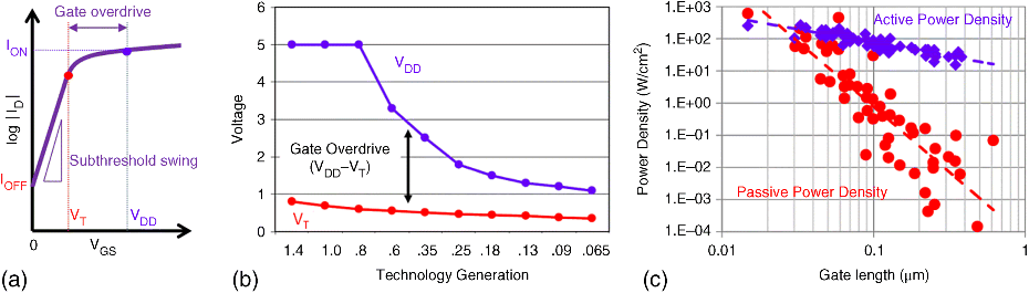
Figure 18.1 (a) Schematic typical ID-VGS of an nMOSFET. The un-scalable subthreshold swing makes IOFF increase exponentially for a linear VT shift towards 0 V. With VT fixed, a reduction of VDD provokes a decrease in ION. (b) VDD and VT scaling down to the 65 nm CMOS technology node [4]. (c) Active and passive power density in ICs for sub-micron gate lengths, and exponential increase of the latter, related to VT reduction [5]
With VT pinned, the gate overdrive had to be reduced and performance sacrificed in order to keep the active power density under control. Although system throughput can be recovered through the use of parallel design (e.g., multi-core processors), a lower bound in total energy per operation is eventually reached when transistors function in the subthreshold regime [6]. Alternative field-effect transistor architectures designed to overcome the subthreshold swing limit of 60 mV/decade at room temperature have been proposed, including the impact ionization MOSFET [7], the tunnel FET [8], the negative-capacitance FET [9] (see Chapter 15). However these solid-state switches still exhibit nonzero leakage currents, hence a subsisting fundamental lower limit in energy efficiency. In contrast, a mechanical relay operating by closing and opening an air gap to switch signal on and off such as illustrated in Figure 18.2, would offer the combined advantages of zero leakage current and extremely abrupt switching behavior.
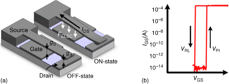
Figure 18.2 (a) Generic planar three-terminal electrostatic switch. (b) Typical measured source–drain current versus gate voltage characteristic for a three-terminal MEM switch
As one might expect from such an intuitive representation of an ideal switch, the use of mechanical relays for computing is not exactly a new idea, and dates back to the late 1930s [10]. Konrad Zuse completed in 1941 the Z3, the world's first functional programmable, fully automated electromechanical computer, switching 2000 relays at frequencies of 5–10 Hz [11]. Almost immediately abandoned in favor of vacuum tubes and solid-state switches, it took several decades worth of technological advances in planar processing, and in particular surface micromachining, to make mechanical computing once again relevant in terms of scalability [12]. This continued progress combined to the emergence of the CMOS power crisis has recently triggered renewed interest in Micro and Nano-ElectroMechanical Systems (M/NEMS) for ultra low power integrated circuits [13,14].
18.1.2 Throughput and Area Efficiency
Various options are available to mechanically open or short an electrical connection between two electrodes, and the constraints associated to fabrication processes may vary according to the type of NEMS switch transduction. Each actuation mechanism also features distinctive advantages and limitations in terms of time and energy required for a switching event. Thus, it is useful to define rough goals in terms of energy–delay trade-off prior to assessing the adequacy of various NEMS relay families for digital logic, which will be the object of Section 18.2.
Today, the intrinsic delay of a single MOS transistor should be on the order of a picosecond. As a rule of thumb, this is three orders of magnitude smaller than what can be expected in terms of mechanical delay due to, for example, an electrostatically actuated relay. This may however not be a showstopper. In CMOS digital ICs, the delay is set by the electrical time constant: stacking devices comes with a quadratic delay penalty, leading circuit designers to buffer and distribute the logical effort over many stages. This is not the case for NEMS relays, for which mechanical inertia dominates over RC delay. In consequence, logic can be implemented using larger, more complex gates where all relays actuate at the same time (single mechanical delay) with in some cases little to no area penalty as device count is reduced [14,15]. Projections suggest that this relay logic could compete with CMOS at the nanoscale [16–18], with typically lower operational frequency but lower energy (Figure 18.3).

Figure 18.3 (a) CMOS to relay logic mapping [14]. (b) Simulated energy–performance trade-off curves for a 30-stage CMOS inverter chain and a 30-relay chain implemented in 65 nm equivalent technologies (based on the ITRS 2007 specifications) [19]
Once again, a lower throughput can be compensated by resorting to massive parallelism. But this is eventually detrimental to area efficiency and therefore cost per operation. Although the manufacturing cost of a NEM switch can arguably be predicted to be lower than, for example, a state of the art FinFET; concluding at this point that NEMS can entirely supplant CMOS for digital logic would be premature. A NEMS-only integration scheme would obviously be the least constrained in terms of process sequence, thermal budget and material selection, but at the risk of confinement to low density, moderate speed applications such as Field-Programmable Gate Arrays (FPGA). Considering the above, trying to keep the NEMS switch technology CMOS-compatible may be more prudent for high-speed digital logic. Because not all transistors in a microprocessor operate at the maximum clock frequency, a NEMS/CMOS co-integration scheme could enable saving energy using relays in the low throughput sub-blocks, while maintaining high-performance where needed.
Monolithic co-integration offers the advantage of reduced interconnect parasitics over a “system in package” approach [20]. MEMS-first integration has considerable handicaps in terms of device scalability and foundry compatibility due to the extensive preprocessing required and resulting increased wafer cost. A MEMS-last process, in which the MEMS fabrication steps are performed after completion of the CMOS back end of line, seems the most attractive. It is however critical that the underlying electronics can withstand the thermal budget of MEMS processing. Transistor characteristics must remain unaffected (avoiding dopant diffusion, equivalent oxide thickness variations), and the metal interconnects should be preserved from via resistance failure and electromigration which may arise from thermal stress and annealing effects. It was shown for example that the thermal budget limit for a 0.25 μm CMOS process was 425 °C for 10 h [21]. This significantly restricts the choice of structural materials available for NEMS fabrication (low temperature oxides, amorphous Silicon, polycrystalline SiGe, etc.).
18.2 Actuation Mechanisms
18.2.1 Electromagnetic
Electromagnetic relays convert a magnetic field into mechanical displacement based on either the Lorentz force or the magnetostrictive effect. Essentially, an inductor and a soft magnetic actuator are required, although the addition of hard magnetic films (permanent magnets) to improve energy efficiency seems unavoidable at the micro and nanoscales (Figure 18.4).
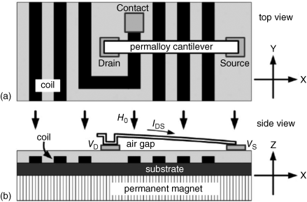
Figure 18.4 (a) Top view and (b) cross-section of an electromagnetic MEM relay, in the on-state [22]. The right side of the movable cantilever is in contact with the source electrode, forming an electrical path between drain and source
Generating a magnetic field can be achieved by flowing current across an inductor such as a Cu coil. For ease of fabrication, planar coils are preferred over their three-dimensional, multi-layered counterparts, in spite of being particularly area consuming. In addition to this, coils do not fare particularly well in terms of energy efficiency at the microscale, so that integrating auxiliary permanent magnets (PM) may be necessary to add a “background” preactuation magnetic field and hence decrease power consumption during switching. As an indicator of how poorly they scale, it can be shown that a tremendous 104 A/mm2 current density is needed for a 100 μm micro-coil to generate the same magnetic moment as a 1 T magnet of same dimensions, with every size reduction by a factor of 10 resulting in an 10-fold increase of the required current density [23]. The most suitable permanent magnet materials include thin film CoPt, FePt, or rare earth-based thick film Nd2Fe14B, SmCo5 [24]. CoPt and FePt processing requires relatively high post deposition annealing temperatures (500–700 °C) for obtaining high coercivity values, which is a major disadvantage for CMOS co-integration. On the other hand, the use of rare earth-based alloys comes with problems of easy oxidation, etching process compatibility and adhesion to Si as well as potential contamination issues.
The most straightforward way to emulate a switch is to subject a soft magnetic film to the Lorentz force. Permalloy (NiFe) cantilevers can be used [22,25] with the following advantages: well-developed technology for deposition and micromachining (owing to the longstanding use of permalloy magnetic heads in the recording industry), high saturation flux density and low hysteresis. Besides, permalloys are immune to the reverse magnetostrictive effect, which causes a change of magnetic properties under mechanical stress. Displacement can also be obtained by taking advantage of the direct magnetostrictive effect, which results in the deformation of some ferromagnetic films upon magnetization. This type of transduction can be used to provoke strain mismatch-induced deflection of a bimorph membrane or cantilever coated by magnetostrictive films [26]. Suitable candidates for such coatings in terms of sensitivity include rare earth TbFe, SmFe thin films or TbFe/FeCo multilayers [26,27].
Without specifically targeting digital logic, magnetic microrelays demonstrators have so far exhibited switching power consumption of the order of 10–100 mW, sub-kHz operating frequency and single device area measured in mm2 [22,25]. To this day, electromagnetic switches do not seem particularly adequate for computing applications because of inherent issues related to area consumption, unconventional processing and insufficient energy efficiency.
18.2.2 Electrothermal
Thermal expansion is the driving phenomenon for electrothermal switches actuation. Two terminals are dedicated to providing power to the actuator through dissipated heat. This can simply be achieved with Joule heating caused by current flowing across a resistive actuating cantilever or beam. Specifically engineered geometry such as a V-beam [28], or thermal expansion coefficient mismatch within a bimorph structure [29,30] causes them to buckle when heated (closing a gap and making contact between two other terminals), and return to their original position once the power is turned off (breaking contact). Thermally actuated relays have been reportedly investigated for a wide range of applications which so far did not include computational logic: switched inductors [29], contact test structures [31], RF MEMS [28] and CMOS power gating for zero standby power [30].
Commonly cited advantages of such devices are high contact forces, large possible displacements and IC-compatible low actuation voltages [28]. High contact forces are typically associated to low contact resistance and therefore low insertion loss which is indeed a significant advantage for RF switches. For logic circuits however, as discussed in Section 18.1.2, the RC delay is typically orders of magnitude lower than the mechanical delay so that lowering the contact resistance is far less critical. This is especially true if its root cause is plastic deformation occurring in the contact regions, which raises additional concerns in terms of reliability (cycling, hysteresis). Large displacements can also be problematic for endurance, due to accelerated structural fatigue. Besides, because actuation is slow (hundreds of microseconds) and high currents are needed to generate sufficient heat, sub-1 V actuation voltages do not prevent thermal micro-relays from consuming around 10 mW for a single switching event [30]. Finally, from the perspective of potential for large-scale integration, the scalability of such switches seems once again fundamentally limited by the transduction mechanism.
Electrothermal NEMS relays do not appear as strong contenders for beyond CMOS computing. They are in some regards comparable to electromagnetic switches, albeit with the undeniable advantage of more conventional material processing.
18.2.3 Piezoelectric
Piezoelectric materials have the ability to charge in response to mechanical stress (this is the direct piezoelectric effect), and reciprocally to deform in response to an electric field (this is the reverse piezoelectric effect). While the former is most useful in resonators for acceleration, pressure or mass sensing [32,33], the latter is exploited in micro-actuators [34]. Because of their use for a particularly broad range of MEMS applications, and even some IC applications such as FeRAM [35], piezoelectric materials process technology has been relatively well developed. Piezoelectricity is also linear (which in itself is interesting for resonators, but of little relevance to logic switches operation) and bi-directional, meaning that displacement on both sides of the equilibrium position is possible depending on the polarity. This last property is very interesting in that it enables active turn-off of a relay, a feature which will be discussed later in Section 18.3.3, and facilitates the implementation of complementary logic.
The most commonly used piezoelectric materials for MEMS are PbZrxTi1−xO3 (PZT), aluminum nitride (AlN) and zinc oxide (ZnO). PZT is known to yield the most efficient transduction, but high quality material availability is limited (need for stoichiometry control with x = 0.53 for maximal efficiency), and it is lead-based, which makes it incompatible with CMOS foundries [36]. AlN-based microrelays have been proposed in particular by researchers at the University of Pennsylvania, first for use as RF switches [37,38] and later for complementary logic [36,39]. These recent studies show variations of the dual beam design illustrated in Figure 18.5 featuring numerous advantages: active turn-off, complementarity, threshold adjustment via body-biasing, immunity to stress-induced out of plane bending, and an actuation mechanism (based on buckling of bimorph beams) which allows overcoming the typically small displacements generated by the reverse piezoelectric effect.
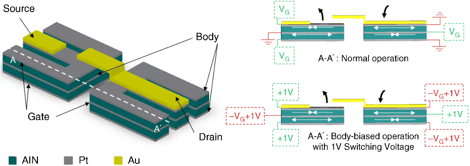
Figure 18.5 (a) 3D schematic and (b) cross-sectional views of the stress-compensated dual beam design from [36] showing body-biased operation. Note that the gap is differentially defined between two cantilevers of same dimensions and structure, hence same deflection at rest. This allows the actuation gap after release to be the same as the sacrificial thickness
A Pt/AlN/Pt/AlN/Pt (200 nm/1 μm/200 nm/1 μm/200 nm) sandwich serves in this case as the structural stack. A gold contact is patterned on top of one of the beams, separated from the top Pt layer of the other beam by a contact air gap defined by a 200 nm amorphous Si sacrificial layer release-etched in vapor phase XeF2. In one of the two opposing beams, the bottom AlN layer is made to longitudinally expand (respectively, contract) through reverse piezoelectric effect, while the top layer is made to contract (respectively, expand), causing the beam to buckle upward (respectively, downward). An Au/Pt contact is made as the two beams meet, transmitting the signal. The beams can be moved apart by changing biasing polarities in the Pt layers (active turn-off). With these switches, sub-1 V operation has been demonstrated thanks to body-biasing (VB = 14 V), with 220 ns switching time, and endurance up to 107 cycles with low contact resistance (<500 Ω) [39]. A complementary relay inverter was also demonstrated at 100 Hz. Remaining challenges include scaling down the vertical and lateral dimensions (the current footprint being around 200 × 200 μm2 per switch), which would improve area efficiency and reduce parasitic capacitances limiting high frequency operation. A different Au-free contacting metal should be implemented to render processing CMOS-compatible, which may change the deal in terms of contact resistance value and stability.
Piezoelectric relays show promise for mechanical computing applications in terms of speed and energy efficiency. CMOS process compatibility and technology scalability are the next roadblocks to address. Encouragingly, recent works on resonators for gravimetric detection have led to demonstrating 50 nm thick AlN films with excellent piezoelectric properties [33].
18.2.4 Piezoresistive
The piezoresistive effect is a change of electrical resistivity in semiconductors upon application of mechanical stress. This property is widely used in strain-enhancement techniques for high-mobility CMOS. Piezoresistive elements can be incorporated in mechanical relays to generate an abrupt switching behavior when combined in series with a supplementary transducer converting an electrical signal into mechanical stress (e.g., piezoelectric, electrostatic, etc.). The appeal of such an approach with added complexity is that it circumvents the obstacle of contact adhesion forces, which may cause hysteretic characteristics or even functional failure in most air gap-based mechanical switches.
Polymers doped with carbon black or metal nanoparticles can also emulate piezoresistivity and although the fundamental mechanism is different, sharp stress-conductivity characteristics can be obtained. MIT researchers introduced a three-terminal mechanical relay consisting of a patterned polydimethylsiloxane (PDMS) pillar containing Ni nanoparticles, and becoming conductive when squeezed by an electrostatically actuated Al membrane, hence the moniker “squitch” [40]. When a sufficient pressure is applied to the nanocomposite, a conduction path is created between the conductive metallic particles and the relay turns on with a theoretical 10−7 Ron/Roff ratio. This architecture faces many practical problems, such as sensitivity to creep, possibility of inter-particle adhesion causing reliability issues upon cycling, and more obviously process integration and scalability.
IBMs PET concept (PiezoElectronic Transistor) relies on the inverse piezoelectric effect to transmit stress to a piezoresistive “channel” [41]. For the stress transfer to be efficient, a yoke made of a high yield material such as SiN should be preventing mechanical displacement of the free boundary of the PR film (Figure 18.6).
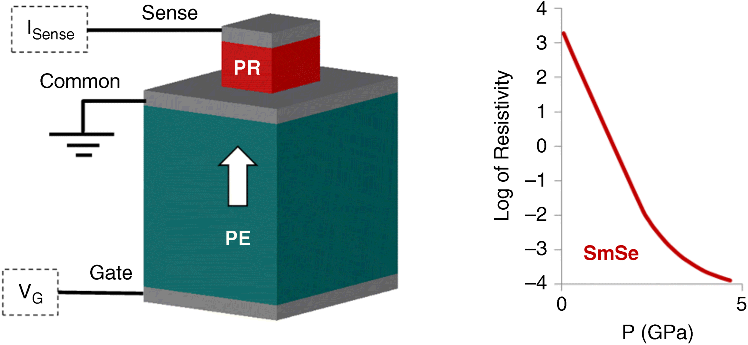
Figure 18.6 Left: PET with three terminals (gate, common, and sense), a piezoelectric element between the common and gate terminals and a piezoresistive element between the common and sense terminals. The constraining mechanical yoke is omitted for clarity. Right: Resistivity–pressure characteristic for a piezoresistive monochalcogenide: SmSe [41]
The best candidates for optimal transduction are believed to be PZN-PT {(1 − x)[Pb(Zn1/3Nb2/3)O3] − x[PbTiO3]} or PMN-PT {(1 − x)[Pb(Mg1/3Nb2/3)O3] − x[PbTiO3]} for the piezoelectric element, and SmSe, TmTe, Eu-doped SmS or Cr-doped V2O3 for the piezoresistive element [41]. In a best case scenario, an analysis of the device's dynamic response indicated an outstanding projected operating frequency of 20 GHz at VDD = 0.1 V. Nevertheless, these numbers rely on many assumptions such as: (i) negligible three-dimensional effects, (ii) lossless stress transfer, and most of all that (iii) these lead-based and rare earth chalcogenide materials can be integrated down to thicknesses of a few nanometers while conserving their sensitivity. Moreover, static analysis shows a 10−4 Ron/Roff ratio for a gate-common bias of 0.18 V, which translates into an equivalent less than ideal subthreshold swing of 45 mV/dec.
Pending further experimental work, it is unclear at this point whether the energy efficiency benefits of piezoresistive switches can eventually be worth the implementation of an extremely disruptive technology with uncertain scalability.
18.2.5 Electrostatic
M/NEM relays utilizing electrostatic actuation may now appear excessively simple in comparison. Although not the most popular for RF switching applications due to relatively low contact forces and high contact resistance [42], these characteristics are not critical for computational purposes, as previously discussed in Section 18.1.2. These switches are essentially based on two conductive layers forming a capacitor: one being fixed and the other movable (e.g., cantilever, clamped–clamped beam, membrane, nanowire). They are therefore generally easy to fabricate with conventional planar processing techniques and conventional, inexpensive, MOS-compatible materials which do not lose their transducing properties at the nanoscale. As the capacitor charges upon applying a potential difference, the attractive electrostatic force (regardless of polarity) deflects and accelerates the movable electrode towards the fixed one. When the actuating bias disappears, the switch can be passively turned off as the spring restoring force causes the movable membrane to return to its original position, breaking the contact. Let us consider the simple model in Figure 18.7, where the top electrode of a parallel-plate capacitor of area A is suspended by a spring of elastic constant k and is separated from a fixed bottom electrode by a distance g.
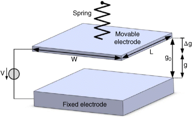
Figure 18.7 Parallel plate capacitor model for electrostatic actuation. g0 is the as-fabricated gap corresponding to the separation at rest
Under a bias V, the electrostatic force Felec and spring force Fspring exerted on the top electrode are [43]:
As the deflection increases, Felec increases superlinearly, whereas the Fspring increase is only linear. Beyond a critical displacement which can be easily derived as g = g0/3, the system becomes unstable, Felec is always superior to Fspring and the switch closes abruptly: this phenomenon is called pull-in. The pull-in voltage Vpi is thus:
In order to keep Vpi low and the switching energy minimal, the spring should be relatively compliant, but it also should be sufficiently stiff to overcome contact adhesion forces. Contact dimples are commonly used in order to minimize the contact area and alleviate this constraint. In this case, it is useful to distinguish between the actuation gap g0 and the contact dimple gap gd. If gd is larger than g0/3, the switch is operating in pull-in mode. A characteristic of pull-in mode is that although the actuated plate does not collapse onto the fixed electrode, the abrupt increase in capacitance when V > Vpi causes an intrinsically hysteretic current–voltage characteristic. In nonpull-in mode (gd < g0/3), the adhesion forces alone may contribute to the hysteresis. It should be noted that there are ways to avoid pull-in instability beyond the g0/3 displacement limit, such as leveraged bending [44] or dynamic charge control (by adding a capacitor in series) [45].
From a dynamic point of view, neglecting contact bouncing and ringing upon contact break, the mechanical delay can be approximated [16] as a function of the fundamental resonant period [2π(m/k)1/2], the dimple to actuation gap ratio (gd/g0), and the “gate overdrive” (VDD/Vpi):
α, β and γ can be numerically derived by solving Newton's second law of motion; their values primarily depend on the quality factor Q of the system and thus on the damping ratio for its first mode of oscillation. χ is an adjustment variable accounting for the dramatic increase of tdelay when VDD/Vpi is very close to 1. Equation 18.3 gives us a sense that to minimize the delay for a given overdrive and gap aspect ratio, the structural material of the actuated electrode should be stiff (high Young's modulus) and light (low density). This is why speed is one of the driving arguments for investigating carbon-based electrostatic switches (Carbon Nano Tubes [46–50], graphene [51], SiC [52,53]). Increased stiffness comes however at the cost of larger Vpi (18.2) and therefore higher switching energy.
If the system is underdamped (Q > 1/2), the oscillations of the movable plate after breaking contact could interfere with the off-state electrical characteristics and therefore set an effective tdelay larger than the previous pull-in-based expression. A cut-off distance gc = 2 nm is generally considered large enough to avoid undesirable tunneling current between electrodes during off-state. Avoiding tunneling after release translates into a condition on the logarithmic decrement of the damped oscillations, which should be larger than ln(gd/gd − gc). Expressed in terms of Q:
Substituting gc = 2 nm, the inequality above results in a surprisingly simple but reasonably accurate rule of thumb stating that the quality factor should be designed to be smaller than the dimple gap gd expressed in nm.
Obviously though, not all of these electrostatic relays can be modeled as parallel plate capacitors, and each design has its specific energy–delay trade-off. The next section is dedicated to the many design variations available to date in the literature for electrostatically actuated NEM relays, their assets and drawbacks.
18.3 Electrostatic Switch Designs
18.3.1 (N > 3)-Terminal Switches
Many different switch designs are reported in the literature, which can be classified by number of terminals typically ranging from two [54] to eight [55]. The majority of them are three-terminal (3-T) relays, which can probably be explained by a natural tendency to mimic the transistor configuration of a control gate allowing signal propagation between two “Source” and “Drain” terminals. However, we have already evoked (Section 18.1.2) the risks of confining NEMS relay applications to CMOS-like logic: this path should probably be avoided unless each relay can switch (mechanical and RC delay) as fast as a transistor, and its individual footprint is comparable to that of a MOSFET.
Pass-gate logic, on the other hand, comes with a reduced device count (compensating for larger individual footprint) and enables switching one complex logic gate with a single mechanical delay. Single MOS transistors are notoriously imperfect devices for pass-gate logic. This is due to their intrinsic inability to “swing full rail” at the output, that is, having the ability to propagate both a logic “0” (VS = 0 V) and a logic “1” (VS = VDD). Because VGS has to be larger than the threshold voltage VT, an nMOSFET can only pass VS from 0 V to VDD-VT (and conversely, a pMOSFET from VT to VDD). The fundamental issue is that the control condition is coupled to the signal to transmit. The same principle applies to 3-T electrostatic switches, but an even more basic argument is that there is no such thing as a 3-T n- or p-relay, because electrostatic actuation is ambipolar. Adding a fourth “Body” electrode permits us to:
- Differentiate “pull-down” and “pull-up” relays.
- Lower the threshold voltage by preactuating the device.
- Decouple control and signal.
An example of a 4-T electrostatic switch with insulated channel attached to the movable electrode [56] is shown in Figure 18.8.
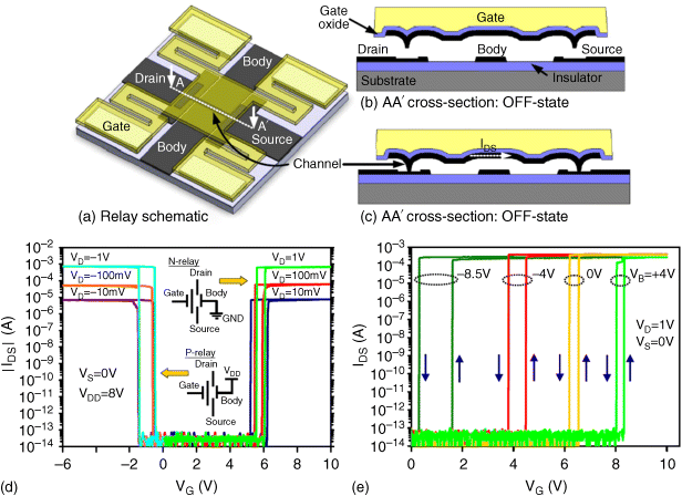
Figure 18.8 Top: (a) Isometric view of a four-terminal relay structure [56]. (b) Cross-sectional view along the channel (AA′) in the off-state. (c) Cross-sectional view in the on-state. When the voltage difference between the gate and body electrodes is sufficiently large (i.e., VGB > Vpi) the body electrode is actuated downward sufficiently to cause the channels – attached to the body electrode via an intermediary oxide layer – to contact their respective S/D electrodes, so that current (ID) can flow between the S/D electrodes. Bottom: Measured IDS-VG characteristics of a single 4-T relay, with VS = 0 V. (d) Operation mimicking that of either an n-channel or a p-channel MOSFET is seen by biasing the body at either 0 V or VDD, respectively. (e) Vpi can be tuned by adjusting VB
One can note that based on the design in Figure 18.8, the number of Source and Drain outputs can easily be increased by attaching more channels to the movable plate, as long as it serves circuit design efficiency and the total equivalent parasitic gate–channels capacitance remains negligible. A 6-T variation [57] with single Gate and a double pair of Source and Drain is the most straightforward implementation, further reducing device count and reducing the area required to implement a complex logic gate by up to a factor of two [58]. Only two of these 6-T devices connected can be used to deliver simultaneously an inverted and noninverted buffered signal (input on the tied gates). The number of gate inputs can also be multiplied to implement (depending on the biasing scheme) AND, OR [59–61] or MAJORITY (2n + 1 inputs, n > 1) [55] gates with a single relay; and each of the above plus their complementary with two relays [61] (Figure 18.9).
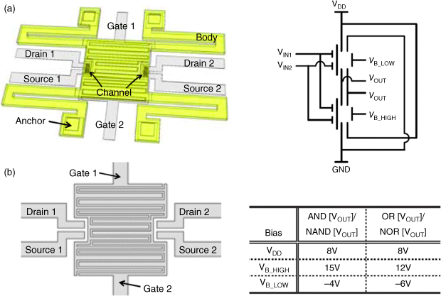
Figure 18.9 Schematic views of a dual-gate, dual-source/drain relay [61]. (a) Isometric view. (b) Bottom electrode layout, showing interdigitated gate electrodes to ensure that they have equal influence on the body. (c) Circuit schematic of a dynamically configurable complementary relay logic circuit utilizing two dual-gate, dual-source/drain relays. (d) Corresponding AND/NAND and OR/NOR bias configurations
18.3.2 In-Plane versus Out-of-Plane Actuation
Considering the substrate as the plane of reference, we have focused so far on out-of-plane deflected switches. There are nonetheless many instances of in-plane-actuated electrostatic NEM relays: [62–67]. For such devices, the gaps are defined by lithography, as opposed to a deposited sacrificial layer thickness. In terms of layout and for a given processing sequence, it means that a broad range of Vpi can be targeted by simply varying the gap width, which has a much lesser impact on device footprint than adjusting the actuation area.
Yet, this supposed ease of design stands under the condition that the structural material of the movable electrode (typically metal, if co-patterned with all other electrodes) can be etched vertically with good anisotropy for a high aspect ratio. This may unfortunately not always be true, and in case of a limited membrane thickness, this loss of actuation area should be recovered by designing very long beams. This would introduce nonlinear spring effects making the pull-in behavior far less predictable (compared to a parallel-plate capacitor model and Equation 18.2) and, ultimately, switch dimensioning more difficult.
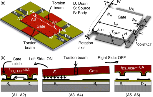
Figure 18.10 (a) Isometric illustration of the seesaw relay structure and definition of design parameters [75]. (b) Schematic cross-sectional views. ON–OFF (illustrated here) and OFF–ON are the two stable states for perfectly complementary operation. The two body electrodes (coplanar with the source/drain electrode pairs) located underneath the gate electrode, one on either side of the torsional axis, are used to apply voltages across the actuation air gap to electrostatically actuate the seesaw beam downward on only one side at a time and thereby turn on the relay on that side and turn off the relay on the other side
Another argument to consider is that while the in-plane actuated switch approach is relatively 3-T friendly, fabricating 4-T relays (for decoupled control and signal, cf. Section 18.3.1) can prove to be more challenging. It can be achieved through the use of less trivial processing steps such as spacer definition of the insulated channel, followed by localized stringer removal to suppress shorts [67].
18.3.3 Active Turn-Off Devices
In the first section of this chapter, a premise was that relays would allow overcoming the fundamental energy limit in CMOS circuits set by subthreshold leakage. However, a legitimate concern in electrostatic NEMS relay design is that hysteretic switching behavior (coupled to the fact that the switch should turn off at 0 V) is also setting a switching energy limit. Even considering an architecture with contact dimples, operating in nonpull-in mode (gd < g0/3), counting on a passive release to break the contact means that the spring restoring force for a displacement gd should be large enough to overcome the contact adhesion force:
Unfortunately, the higher the spring constant k, the higher Vpi becomes (Equation 18.2). We have seen in Section 18.2.4 that piezoresistive relays could circumvent contact adhesion force issues by escaping from the conventional “physical contact make/break” scheme, but were not necessarily infinitely abrupt, zero-leakage (and depending on the choice of the piezoresistive material, not always hysteresis-free) switches.
A single-pole double-throw (SPDT) configuration is fairly common for in-plane actuated relays, because the design is straightforward. One actuating fixed electrode can be laid out on each side of the pole, and each can be used to break a contact occurring on the other side [50,63,66,67]. A notable out-of-plane SPDT variation called torsion microactuator or see-saw relay was initially designed for low voltage RF switches used for instance in passive phase shifters [68–71]. The motivation was the same as stated above: reducing the losses (power consumption) through using beams of lesser stiffness which would otherwise remain stuck down by adhesion forces.
A movable electrode is anchored along one of its coplanar symmetry axes. A fixed electrode is placed on each side of this axis under each half of the movable plate, so that it can swing on either side of the torsional axis depending on fixed electrode biasing scheme. The pull-in behavior of such devices can be predicted analytically with good accuracy [72,73]. What makes them particularly interesting for logic circuits is their built-in switching complementarity. Besides, it is possible to demonstrate switching symmetry about VDD/2, which is advantageous for symmetric noise margins [74]. An example of a 7-T design with two insulated channels [75] is shown in Figure 18.10.
Pointing out that active turn-off consumes power is a tautology; at best this feature can help to lower the energy limit set by adhesion force. Compared to a spring-driven passive release, a see-saw relay is energy-efficient in cases where the contact adhesion energy on one side is larger than the amount required for pulling the other side down. Regarding the latter, see-saws have the handicap of showing a larger gap before actuation than the nominally defined gap (as-deposited sacrificial layer thickness), because this side is deflected upward when the other is touching down. This implies that minimal excursion of the movable plate should be targeted when toggling between on and off states, with extremely scaled contact dimple gaps.
18.4 Reliability and Scalability
18.4.1 Contact Stability
Even though mechanical delay is predominant in relay switching dynamics, the electromechanical (EM) contact resistance remains an important figure of merit for circuit design, because it determines how many simultaneously switched stages can be cascaded with no speed penalty. It is therefore critical that its value should remain stable upon cycling. This is true as well for the contact surface topology: plastic deformation of asperities following repeated impacts can modify the adhesion force, potentially leading to permanent stiction failure. This particular failure mode may also be caused by micro welding depending on the current density when the relay is in the on-state. The reliability requirements are largely dependent on the type of application. For example, it can be estimated that the on-state contact resistance of a switch should be kept below 100 kΩ for over 1014 cycles so that a relay-based microcontroller for embedded sensor applications could operate reliably for 10 years at up to 100 MHz with a transition probability of 1% [17].
It is essential to properly understand the physics of electromechanical contacts at the nanometer scale in order to select the appropriate materials, design and surface treatments needed to meet the performance and stability specifications. In practice, the contacting electrodes are almost never ideally flat, and the effective contact area Aa between two conductive rough surfaces is only a fraction of the apparent dimensions (e.g., as drawn on a lithographic mask). Physical contact is only made at some asperities, each having its own associated load (pi), local area (ai) and local current (ii; Figure 18.11).
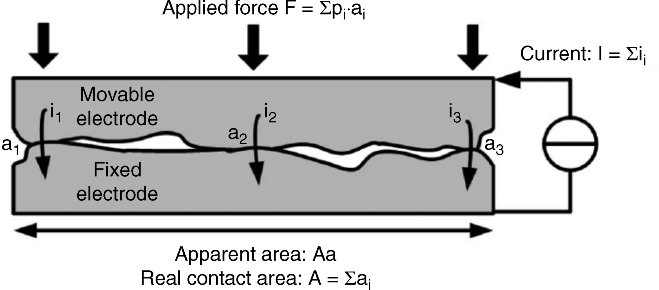
Figure 18.11 Cross-sectional schematic of an EM contact, showing three asperities (called α spots) where current can flow. Total load P and current I correspond to the sum of the contributions from every α spot
The constriction resistance Rc at each microcontact (arising from the convergence and divergence of the current flow) can be described by a size-dependent expression [76]:
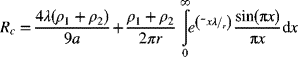
ρ1 and ρ2 are the specific resistivities of the contacting surfaces 1 and 2, λ = (λ1 + λ2)/2 is the average electron mean free path, r is the radius of the microcontact of area a. When r < λ, the expression reduces to Sharvin's point-contact model [77]: electrons are assumed to ballistically travel across the contact without being subjected to scattering and RS ≈ λ(ρ1 + ρ2)/2a. If r > λ, Equation 18.6 approaches the other limit case, Holm's resistance [78], for which the constriction resistance is dominated by scattering RH ≈ (ρ1 + ρ2)/4r.
As the contact force is increased asperities can be deformed, causing the real contact area to increase, which in turn lowers the total EM contact resistance. This might seem beneficial at first glance but it should be noted that the flattening of asperities has some undesirable side-effects: increased real contact area and reduced separation of the noncontacting regions (which contribute to adhesion via van der Waals forces). As a consequence, hysteretic behavior is aggravated, possibly to the point of permanent stiction. Besides, for a fixed bias between the two contacting electrodes; a decreasing resistance leads to an increase in dissipated power (P = V2/R), heating the contact as a result, which accelerates its deformation and makes it prone to micro-welding.
In order to prevent permanent mechanical wear, the contact load should be sufficiently low (typically < 100 μN) to avoid causing plastic deformation of the electrode material. Selecting a contacting material of high Mohs hardness (>6) can also be useful. The stronger metallic bonds typically associated to hard materials [79] should not be detrimental to adhesion at this scale, because van der Waals interactions are believed to remain dominant (contacting small asperities in the elastic regime). Unlike for RF switching, the contact resistance does not have to be very low for digital logic applications, so the fact that the real contact area remains small is not a critical concern either. Iridium (Ir), rhodium (Rh), ruthenium (Ru), and tungsten (W), being hard metals, are therefore suitable candidates from a strictly electromechanical point of view.
However, extrinsic environmental contamination effects can be another important source of contact resistance instability. Late transition metals (Ir, Rh, Ru) are active catalysts and have been observed to cause the formation of friction polymers on and around the contacting surfaces [80] even in a reasonably clean, packaged environment [81]. This shows that extreme attention should be paid to removing any residual process-induced hydrocarbon contaminants (such as photoresist, or plasma etch byproduct). Tungsten has been shown to be significantly prone to oxidation, limiting the contact lifetime even under high vacuum [82].
Surface passivation techniques can be used to remedy these contamination issues. A few monolayers of conductive metal oxides such as TiO2 can be deposited via Atomic Layer Deposition to coat W contacting electrodes after sacrificial layer release, thus improving reliability. This implies trading off some of the nominal contact resistance, but thanks to a moderate potential barrier for electrons at the W/TiO2 interface, Rc may still fall within the 100 kΩ specifications [19]. Some other metals such as ruthenium or iridium can naturally grow a conductive oxide (RuO2, IrO2) when annealed in oxygen, which has the advantage of being localized as opposed to a nonselective ALD which may affect surface leakage. 2 nm RuO2 can be thermally grown on pure sputtered Ru following a 2 h low temperature thermal oxidation at 420 °C [83]. The Ru/RuO2 system seems promising so far for enhancing contact stability, although a practical implementation of this relatively unusual metal raises various process integration considerations such as ease of deposition onto other layers, film adhesion, ease of etching, stress compatibility, and of course overall cost of fabrication.
18.4.2 Process Scalability and Perspectives
We have seen in Section 18.2 that electrostatically-actuated NEMS relays were arguably among the most scalable switches. Later (Section 18.3), basic operating principles of the simplified parallel-plate actuator model showed that the ultimate limits in terms of energy efficiency and delay can be attributed to inter-related parameters:
- The system's spring constant – low k for low Vpi, high k and low mass for small delay.
- The actuation and contact gap – small excursion for low Vpi, large excursion for larger Fspring.
- The contact properties – low but stable contact resistance with adhesion force smaller than Fspring.
One possible route for balancing trade-offs (i) and (ii) can consist of simultaneously opting for high spring constant and small contact gap. This is the strategy motivating the use of low density, high Young's modulus, ultimately thin structural materials such as Carbon nanotubes or graphene [84,85]. Nevertheless, it should be stressed that fabricating CNT or graphene-based nanorelays with insulated control (“Gate”) and transmitting electrodes (“Source and Drain”) appears extremely challenging, which could be a handicap in terms of circuit design optimization. An alternative solution may be using extremely thin amorphous metal films (e.g., deposited by ALD), the associated issue being residual stress management. In the case of out-of-plane actuated switches, residual stress can cause the movable electrode to buckle, altering the nominal gap value. This can be addressed by resorting to multi-layer structural stacks for stress compensation, or scaling the lateral dimensions to prevent out-of-plane deflection from building up [57], at the respective costs of increased mass (hence tdelay) and reduced capacitance (thus higher Vpi).
Releasing nanometer-scale gaps is not trivial. One of the most common configurations is sacrificial SiO2 selectively etched in HF. Water is a byproduct (and catalyst) of this reaction, which may cause stiction upon release due to capillarity forces. By using a critical point dryer, 15 nm gaps could be released, undercutting relatively short TiN cantilevers [86]. Anhydrous HF release at reduced pressure (75 Torr) has led to the same results on poly-SiGe membranes with lateral dimensions of several microns [88]. Although process controllability has yet to be demonstrated, some design tricks can enable to release tiny contact gaps as small as 4 nm [54]. Volume-shrinkage induced gap formation processes based on silicidation are also a promising novel alternative for high aspect-ratio structure releases [88].
Item (iii) has been addressed in the previous subsection. Yet, it is worth pointing out that the multiple-asperity-based constriction resistance model might no longer stand for ultimately scaled contact dimensions [89]. Hard contacting electrodes would still be desirable for their resistance to plastic deformation in a “single-asperity” configuration, but the adhesion force would become dominated by metallic bonding (instead of van der Waals interactions). Since hard materials are usually characterized by high metallic bonding energies, surface treatment schemes (hydrogen passivation, controlled oxidation, ALD coating, use of self-assembled monolayers) to decrease the adhesion force are likely to be required at this scale.
Considering the tremendous progress accomplished recently in the fields of material sciences and technological processes for M/NEMS fabrication dedicated to advances in device and circuit design, the odds of an emergence of nanoscale mechanical computing to alleviate the CMOS power crisis are better than ever.
References
- 1. Dennard, R.H., Gaensslen, F.H., Rideout, V.L. et al. (1974) Design of ion-implanted MOSFET's with very small physical dimensions. Journal of Solid-State Circuits, SC-9(5), 256–268.
- 2. Baccarani, G., Wordeman, M.R., and Dennard, R.H. (1984) Generalized scaling theory and its application to a 1/4 micrometer MOSFET design. IEEE Transactions on Electron Devices, 31(4), 452–462.
- 3. Davari, B., Dennard, R.H., and Shahidi, G.G. (1995) CMOS scaling for high performance and low power - The next ten years. Proceedings of the IEEE, 83(4), 595–606.
- 4. Packan, P. (2007) Device and Circuit Interactions (Short Course), Proc. Int. Electron Devices Meeting, 2007.
- 5. Meyerson, B. (2004) Proc. Semico Impact Conference 2004.
- 6. Calhoun, B.H. and Chandrakasan, A. (2004) Characterizing and modeling minimum energy operation for subthreshold circuits, Proc. Int. Symp. Low-Power Electron. Design, 2004, pp. 90–95.
- 7. Gopalakrishnan, K., Griffin, P.B., and Plummer, J.D. (2002) I-MOS: A novel semiconductor device with a subthreshold slope lower than kT/q, Proc. Int. Electron Devices Meeting, 2002, pp. 289–292.
- 8. Reddick, W.M. and Amaratunga, G.A.J. (1995) Silicon surface tunnel transistor. Applied Physics Letters, 67, 494–496.
- 9. Salahuddin, S. and Datta, S. (2008) Can the subthreshold swing in a classical FET be lowered below 60 mV/decade?, Proc. Int. Electron Devices Meeting, 2008, pp. 693–696.
- 10. Shannon, C.E. (1938) A symbolic analysis of relay and switching circuits. Transactions AIEE, 57, 713–723.
- 11. Zuse, K. (1993) The Computer - My Life, Springer-Verlag.
- 12. Petersen, K.E. (1978) Dynamic micromechanics on silicon: Techniques and devices. IEEE Transactions on Electron Devices, 25(10), 1241–1250.
- 13. Akarvardar, K., Elata, D., Parsa, R. et al. (2007) Design considerations for complementary nanoelectromechanical logic gates, Proc. Int. Electron Devices Meeting, 2007, pp. 299–302.
- 14. Chen, F., Kam, H., Markovic, D. et al. (2008) Integrated circuit design with NEM relays, Proc. Int. Conf. Comput.-Aided Design, 2008, pp. 750–757.
- 15. Chen, F., Spencer, M., Nathanael, R. et al. (2010) Demonstration of integrated micro-electro-mechanical switch circuits for VLSI applications, Proc. Int. Solid State Circuits Conf., 2010, pp. 26–28.
- 16. Kam, H., Liu, T.-J.K., Stojanovic, V. et al. (2011) Design, optimization, and scaling of MEM relays for ultra-low-power digital logic. IEEE Transactions on Electron Devices, 58(1), 236–250.
- 17. Pott, V., Kam, H., Nathanael, R. et al. (2010) Mechanical computing redux: relays for integrated circuit applications. Proceedings of the IEEE, 98(12), 2076–2094.
- 18. Spencer, M., Chen, F., Wang, C.C. et al. (2011) Demonstration of Integrated Micro-electro-mechanical relay circuits for VLSI applications. IEEE Transactions on Electron Devices, 46(1), 308–320.
- 19. Kam, H., Pott, V., Nathanael, R. et al. (2009) Design and reliability of a micro-relay technology for zero-standby-power digital logic applications, Proc. Int. Electron Devices Meeting, 2009, pp. 809–812.
- 20. Fedder, G.K., Howe, R.T., Liu, T.-J.K., and Quevy, E. (2008) Technologies for cofabricating MEMS and electronics. Proceedings of the IEEE, 96(2), 306–322.
- 21. Takeuchi, H., Wun, A., Sun, X. et al. (2005) Thermal budget limits of quarter-micrometer foundry CMOS for post-processing MEMS devices. IEEE Transactions on Electron Devices, 52(9), 2081–2086.
- 22. Ruan, M., Chen, J., and Wheeler, C.B. (2001) Latching microelectromagnetic relays. Sensors and Actuators A, 91, 346–350.
- 23. Niarchos, D. (2003) Magnetic MEMS: Key issues and some applications. Sensors and Actuators A, 109, 166–173.
- 24. Chin, T.-S. (2000) Permanent magnet films for applications in microelectromechanical systems. Journal of Magnetism and Magnetic Materials, 209, 75–79.
- 25. Tilmans, H.A.C., Fullin, E., Ziad, H. et al. (1999) A fully-packaged electromagnetic microrelay, Proc. Int. Conf. Microelectromech. Syst., 1999, pp. 25–30.
- 26. Honda, T., Hayashi, Y., Yamaguchi, M., and Arai, K.I. (1994) Fabrication of thin-film actuators using magnetostriction. IEEE Translation Journal on Magnetics in Japan, 9(6), 27–32.
- 27. Ludwig, A. and Quandt, E. (2000) Giant magnetostrictive thin films for applications in microelectromechanical systems. Journal of Applied Physics, 78(9), 4691–4695.
- 28. Wang, Y., Li, Z., McCormick, D.T., and Tien, N.C. (2003) A micromachined RF microrelay with electrothermal actuation. Sensors and Actuators A, 103, 231–236.
- 29. Zhou, S., Sun, X.-Q., and Carr, W.N. (1997) A micro variable inductor chip using MEMS relays, Proc. Int. Conf. Solid State Sens. Actuators, 1997, pp. 1137–1140.
- 30. Raychowdhury, A., Kim, J.I., Peroulis, D., and Roy, K. (2006) Integrated MEMS switches for leakage control of battery operated systems, Proc. Custom Integr. Circuits Conf., 2006, pp. 457–460.
- 31. Kruglick, E.J.J. and Pister, K.S.J. (1999) Lateral MEMS microcontact considerations. Journal of Microelectromechanical Systems, 8, 264–271.
- 32. Karabalin, R.B., Matheny, M.H., Feng, X.L. et al. (2009) Piezoelectric nanoelectromechanical resonators based on aluminum nitride thin films. Applied Physics Letters, 95, 103111.
- 33. Ivaldi, P., Abergel, J., Matheny, M.H. et al. (2011) 50 nm thick AlN film-based piezoelectric cantilevers for gravimetric detection. Journal of Micromechanics and Microengineering, 21, 085023.
- 34. Baborowski, J. (2004) Microfabrication of piezoelectric MEMS. Journal of Electroceramics, 12, 33–51.
- 35. Auciello, O., Scott, J.F., and Ramesh, R. (1998) The physics of ferroelectric memories. Physics Today, 51, 22–27.
- 36. Sinha, N., Jones, T.S., Guo, Z., and Piazza, G. (2009) Body-biased complementary logic implemented using AlN piezoelectric MEMS switches, Proc. Int. Electron Devices Meeting, 2009, pp. 813–816.
- 37. Sinha, N., Mahameed, R., Zuo, C. et al. (2008) Dual beam actuation of piezoelectric AlN RF MEMS switches integrated with AlN contour-mode resonators, Proc. Solid-State Sens. Actuators Microsyst. Workshop, 2008, pp. 22–25.
- 38. Mahameed, R., Sinha, N., Pisani, M.B., and Piazza, G. (2008) Dual-beam actuation of piezoelectric AlN RF MEMS switches monolithically integrated with AlN contour-mode resonators. Journal of Micromechanics and Microengineering, 18, 1–11.
- 39. Sinha, N., Guo, Z., Tazzoli, A. et al. (2012) 1 Volt digital logic circuits realized by stress-resilient AlN parallel dual-beam MEMS relays, Proc. 2012 IEEE 25th Int'l Conference on MEMS, pp. 668–671.
- 40. Paydavosi, S., Yaul, F.M., Wang, A.I. et al. (2012) MEMS switches employing active metal-polymer nanocomposites, Proc. 2012 IEEE 25th Int'l Conference on MEMS, pp. 180–183.
- 41. Newns, D., Elmegreen, B., Liu, X.H., and Martyna, G. (2012) A low-voltage high-speed electronic switch based on piezoelectric transduction. Journal of Applied Physics, 111, 084509.
- 42. Rebeiz, G.M. (2003) RF MEMS: Theory, Design, and Technology, Wiley, New York.
- 43. Senturia, S.D. (2001) Microsystem Design, Springer-Verlag., New York.
- 44. Seeger, J.I. and Boser, B.E. (1999) Dynamics and control of parallel-plate actuators beyond the electrostatic instability, Proc. Transducers, 1999, pp. 474–477.
- 45. Hung, E.S. and Senturia, S.D. (1999) Extending the travel range of analog-tuned electrostatic actuators. Journal of Microelectromechanical Systems, 8(4), 497–505.
- 46. Lee, S.W., Lee, D.S., Morjan, R.E. et al. (2004) A three-terminal carbon nanorelay. Nano Letters, 4, 2027–2030.
- 47. Rueckes, T., Kim, K., Joselevich, E. et al. (2000) Carbon nanotube-based nonvolatile random access memory for molecular computing. Science, 289, 94–97.
- 48. Dujardin, E., Derycke, V., Goffman, M.F. et al. (2005) Self-assembled switches based on electroactuated multiwalled nanotubes. Applied Physics Letters, 87, 193107.
- 49. Dagdour, H., Cassell, A.M., and Banerjee, K. (2008) Scaling and variability analysis of CNT-based NEMS devices and circuits with implications for process design, Proc. Int. Electron Devices Meeting, 2008, pp. 529–532.
- 50. Cao, J., Vitale, W.A., and Ionescu, A.M. (2012) Self-assembled nano-electro-mechanical tri-state carbon nanotube switches for reconfigurable integrated circuits, Proc. 2012 IEEE 25th Int'l Conference on MEMS, pp. 188–191.
- 51. Kim, S.M., Song, E.B., Lee, S. et al. (2011) Suspended few-layer graphene beam electromechanical switch with abrupt on-off characteristics and minimal leakage current. Applied Physics Letters, 99, 023103.
- 52. Lee, T.-H., Bhunia, S., and Mehregany, M. (2010) Electromechanical computing at 500°C with Silicon Carbide. Science, 329, 1316–1318.
- 53. Feng, X.L., Matheny, M.H., Zorman, C.A. et al. (2010) Low voltage nanoelectromechanical switches based on Silicon Carbide nanowires. Nano Letters, 10, 2891–2896.
- 54. Lee, J.O., Song, Y.-H., Kim, M.-W. et al. (2013) A sub-1-volt nanoelectromechanical switching device. Nature Nanotechnology, 8, 36–40.
- 55. Jeon, J., Hutin, L., Jevtic, R. et al. (2012) Multiple-Input Relay Design for More Compact Implementation of Digital Logic Circuits. Electron Device Letters, 33(2), 281–283.
- 56. Nathanael, R., Pott, V., Kam, H. et al. (2009) 4-terminal relay technology for complementary logic, Proc. Int. Electron Devices Meeting, 2009, pp. 223–226.
- 57. Chen, I.-R., Hutin, L., Park, C. et al. (2012) Scaled micro-relay structure with low strain gradient for reduced operating voltage. ECS Transactions, 45(6), 101–106.
- 58. Liu, T.-J.K., Hutin, L., Chen, I.-R. et al. (2012) Recent progress and challenges for relay logic switch technology, Proc 2012 VLSI Tech. Symp., pp. 43–44.
- 59. Hirata, A., Machida, K., Kyuragi, H., and Maeda, M. (2000) A electrostatic micromechanical switch for logic operation in multichip modules on Si. Sensors and Actuators A, 80, 119–125.
- 60. Tsai, C.-Y., Kuo, W.-T., Lin, C.-B., and Chen, T.-L. (2008) Design and fabrication of MEMS logic gates. Journal of Micromechanics and Microengineering, 18, 045001.
- 61. Nathanael, R., Jeon, J., Chen, I.-R. et al. (2012) Multi-input/multi-output relay design for more compact and versatile implementation of digital logic with zero leakage, Proc. VLSI Technology, Systems, and Applications (VLSI-TSA) 2012.
- 62. Chong, S., Akarvardar, K., Parsa, R. et al. (2009) Nanoelectromechanical (NEM) relays integrated with CMOS SRAM for improved stability and low leakage, Proc. Int. Conf. Comput.-Aided Design, 2009, pp. 478–484.
- 63. Czaplewski, D.A., Patrizi, G.A., Kraus, G.M. et al. (2009) A nanomechanical switch for integration with CMOS logic. Journal of Micromechanics and Microengineering, 19, 085003.
- 64. Chong, S., Lee, B., Mitra, S. et al. (2012) Integration of nanoelectromechanical relays with Silicon nMOS. IEEE Transactions on Electron Devices, 59(1), 255–258.
- 65. Chong, S., Lee, B., Parizi, K.B. et al. (2011) Integration of nanoelectromechanical (NEM) relays with Silicon CMOS with functional CMOS-NEM circuit, Proc. Int. Electron Devices Meeting, 2011, pp. 701–704.
- 66. Parsa, R., Shavezipur, M., Lee, W.S. et al. (2011) Nanoelectromechanical relays with decoupled electrode and suspension, Proc. Microelectromech. Syst. Conf., 2011, pp. 1361–1364.
- 67. Lee, W.S., Chong, S., Parsa, R. et al. (2011) Dual sidewall lateral nanoelectromechanical relays with beam isolation, Proc. Transducers, 2011, pp. 2606–2609.
- 68. Milanovi, V., Maharbiz, M., Singh, A. et al. (2000) Microrelays for batch transfer integration in RF systems, Proc. Int. Conf. Microelectromech. Syst., 2000, pp. 787–792.
- 69. Hah, D., Yoon, E., and Hong, S. (2000) A low-voltage actuated micromachined microwave switch using torsion springs and leverage. IEEE Transactions on Microwave Theory and Techniques, 48(12), 2540–2545.
- 70. Kim, J., Kwon, S., Jeong, H. et al. (2009) A stiff and flat membrane operated DC contact type RF MEMS switch with low actuation voltage. Sensors and Actuators A, 153, 114–119.
- 71. Plotz, F., Michaelis, S., Aigner, R. et al. (2001) A low-voltage torsional actuator for application in RF-microswitches. Sensors and Actuators A, 92, 312–317.
- 72. Degani, O., Socher, E., Lipson, A. et al. (1998) Pull-in study of an electrostatic torsion microactuator. Journal of Microelectromechanical Systems, 7, 373–379.
- 73. Degani, O. and Nemirovsky, Y. (2002) Design considerations of rectangular electrostatic torsion actuators based on new analytical pull-in expressions. Journal of Microelectromechanical Systems, 11(1), 20–26.
- 74. Jeon, J., Pott, V., Kam, H. et al. (2010) Seesaw relay logic and memory circuits. Journal of Microelectromechanical Systems, 19(4), 1012–1014.
- 75. Jeon, J., Pott, V., Kam, H. et al. (2010) Perfectly complementary relay design for digital logic applications. Electron Device Letters, 31, 371–373.
- 76. Kogut, L. and Komvopoulos, K. (2003) Electrical contact resistance theory for conductive rough surfaces. Journal of Applied Physics, 94, 3153–3162.
- 77. Sharvin, Y.V. (1965) A possible method for studying Fermi surfaces. Soviet Physics - JETP, 21, 655.
- 78. Holm, R. (1999) Electric Contacts: Theory and Application, Springer-Verlag., Berlin, Germany.
- 79. Courtney, T.H. (1990) Mechanical Behavior of Materials, Mc-Graw Hill., New York.
- 80. Lee, H., Coutu, R.A., Mall, S., and Leedy, K.D. (2006) Characterization of metal and metal alloy films as contact materials in MEMS switches. Journal of Micromechanics and Microengineering, 16, 557–563.
- 81. Czaplewski, D.A., Nordquist, C.D., Dyck, C.W. et al. (2012) Lifetime limitations of ohmic, contacting RF MEMS switches with Au, Pt and Ir contact materials due to the accumulation of ‘friction polymer’ on the contacts. Journal of Micromechanics and Microengineering, 22(10), 105005.
- 82. Chen, Y., Nathanael, R., Jeon, J. et al. (2012) Characterization of contact resistance stability in MEM relays with Tungsten electrodes. Journal of Microelectromechanical Systems, 21(3), 511–513.
- 83. de Boer, M.P., Czaplewski, D.A., Baker, M.S. et al. (2012) Design, fabrication, performance and reliability of Pt- and RuO2-coated microrelays tested in ultra-high purity gas environments. Journal of Micromechanics and Microengineering, 22(10), 105027.
- 84. Loh, O.Y. and Espinosa, H.D. (2012) Nanoelectromechanical contact switches. Nature Nanotechnology, 7, 283–295.
- 85. Loh, O., Wei, X., Sullivan, J. et al. (2011) Carbon-Carbon contacts for robust nanoelectromechanical switches. Advanced Materials, 24, 2463–2468.
- 86. Jang, W.W., Lee, J.O., Yoon, J.-B. et al. (2008) Fabrication and characterization of a nanoelectromechanical switch with 15-nm thick suspension air gap. Applied Physics Letters, 92, 103110.
- 87. Kwon, W., Jeon, J., Hutin, L., and Liu, T.-J.K. (2012) Electromechanical diode cell for cross-point nonvolatile memory arrays. Electron Device Letters, 33(2), 131–133.
- 88. Hung, L.-W. and Nguyen, C.T.-C. (2010) Silicide-based release of high aspect-ratio microstructures, Proc. 2010 IEEE 23rd Intl Conference on MEMS, pp. 120–123.
- 89. Pawashe, C., Lin, K., and Kuhn, K.J. (2013) Scaling limits of electrostatic nanorelays. IEEE Transactions on Electron Devices, 60(9), 2936–2942.