
8
Redox-based Resistive Memory
Stephan Menzel2, Eike Linn1, and Rainer Waser1,2
1Institute of Electronic Materials II, RWTH Aachen University, Germany
2Peter Grünberg Institut (PGI-7), Forschungszentrum Jülich, Germany
8.1 Introduction
Redox-based resistive memories (ReRAM) are a highly promising class of emerging memories [1]. ReRAM cells offer nonvolatile data storage in terms of at least two different resistances, a high resistive state (HRS) and a low resistive state (LRS). By applying appropriate voltage pulses one can switch between these resistance states. Intermediate states are feasible, too, enabling multilevel operation modes. ReRAM cells consist of a simple to fabricate Metal–Isolator–Metal (MIM) stack (see Figure 8.1), in which the insulator is an ion conductor at high fields and/or high temperature. These stacks enable 3D stackable crossbar array architectures. However, simple 1R array implementations suffer from the sneak path problem. Thus ReRAMs cells either require a two-terminal select device (1S1R or 1 CRS) in a passive crossbar architecture configuration, or a select transistor (1T1R) in an active memory matrix (Figure 8.1). The individual ReRAMs cells offer a high scaling potential below feature sizes of F < 10 nm, retention times >10 years, and excellent endurance properties (>1012 cycles). In this chapter we will give an overview of the present knowledge of the physical switching mechanism, the modeling of ReRAMs and the state of the art of device performance.
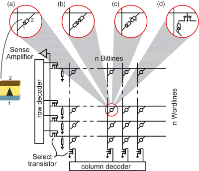
Figure 8.1 Redox-based resistive memory matrix and external CMOS periphery (decoders and sense amplifiers). In the memory array either (a) a single ReRAM cell (1R), (b) a complementary resistive switchs (1CRS), (c) a selector plus ReRAM cell (1S1R), or (d) a transistor plus ReRAM cell (1T1R) is present at each junction of word and bit lines
Although all ReRAM cells are based on redox processes the actual device behavior strongly depends on the applied materials [2]. Hence, it is reasonable to define three subclasses (compare Figure 8.2) [3]:
- Electro-chemical metallization (ECM) cells
- Valency change mechanism (VCM) cells
- Thermo-chemical mechanism (TCM) cells.
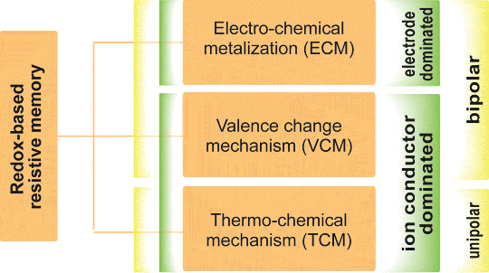
Figure 8.2 Classification scheme for redox-based resistive memory. The memory cells are either dominated by the sandwiched material (VCM and TCM) or by the electrode material (ECM). An alternative classification is based on the I-V characteristic which can be unipolar (TCM) or bipolar (VCM, ECM) Reproduced with permission from [3], © 2012 Wiley-VCH
ECM cells are dominated by the electrodes, offering an active Cu or Ag electrode on one side and an inert (e.g., Pt, TiN) electrode on the other. In contrast, VCM and TCM cells are dominated by the sandwiched material, that is, the chalcogenide (e.g., TaO2, SrTiO3). From an application perspective, the polarity of I-V characteristic – either bipolar (ECM, VCM) or unipolar (TCM) – is also suited for classifying ReRAM devices.
For practical memories one will either use ECM or VCM cells since power consumption is much lower compared to TCM cells and endurance properties are superior. Hence, we will restrict our considerations to ECM and VCM cells in this chapter. In Section 8.2 we describe the physical fundamentals of redox memories and highlight the common generic properties of all redox devices in terms of conduction mechanism, generic switching properties, and dynamical device modeling. In Sections 8.3 and 8.4 we then emphasize the specific features of ECM and VCM, respectively. Finally, exemplary devices offering the excellent performance in the categories feature size, cell area, switching time retention time, write cycles, and multilevel feasibility are presented in Section 8.5.
8.2 Physical Fundamentals of Redox Memories
ECM and VCM cells are based on the same basic physical processes, which are discussed in this section. The most relevant processes in describing/modeling the resistive switching behavior are the conduction mechanisms in HRS and LRS as well as the processes determining the switching kinetics. In addition, ReRAMs show some generic switching characteristics that are related to the nonlinear switching kinetics. These physical fundamentals and switching characteristics build up the basis for modeling ReRAMs. A critical overview of the various modeling activities is given at the end of this section.
8.2.1 Electronic Conduction Mechanisms
The I-layer in ReRAMs is a mixed ionic electronic conductor (MIEC). Typically, the electronic conductivity dominates and accounts for the resistance states of the ReRAM. This is always true in the LRS, whereas the ionic conductivity can be higher in the HRS in some ECM systems, for example, in Cu/SiO2/Pt cells [4]. The ionic conductivity is very low, but the motion of ions triggers the resistive switching effect. In this subsection, we focus on the electronic current contribution. The possible electronic conduction processes in MIM structures are illustrated in Figure 8.3. It can be distinguished between interface and bulk dominated conduction processes. The former are: (i) electron tunneling into the conduction band, (ii) thermionic emission, (iii) direct tunneling from electrode to electrode, and (iv) electron injection into trap states. As bulk related processes (v) electron hopping, (vi) electron tunneling from trap to trap, (vii) band conduction, or (viii) Poole–Frenkel emission might occur. In a real MIM device various conduction processes are always present simultaneously with different balance, which depends also on temperature, applied electric field, and voltage polarity. During the resistive switching process this balance changes. The dominating conduction mechanism might change, for example, from thermionic emission to ohmic conduction. Alternatively, the dominating conduction mechanism might stay the same and only the current density level changes. For example, the thermionic emission barrier and in turn the current density level is altered by the variation of the doping concentration close to the interface due to the Schottky effect. In VCM cells oxygen vacancies (or cation interstitials) can be shallow donors or create deep trap level within the band gap. Changing the amount or distribution of oxygen vacancies thus modifies the cell resistance. The bulk related resistance or electronic transport mechanism is related to oxygen vacancy concentration, which is linked to the conduction center concentration within the insulator. Reference [5] discriminates between five different transport mechanisms. If the oxygen vacancy concentration and in turn the conduction center concentration is below a percolation threshold, the conduction centers are separated from each other and the oxide is in an insulating state. By increasing the oxygen vacancy concentration a percolation threshold is reached increasing the conductivity. By a further increase of conduction centers the conduction mechanism changes to strongly localized nearest neighbor hopping, weakly localized variable range electron hopping, and finally to a metallic conduction mechanism.
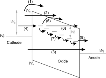
Figure 8.3 Possible electronic conduction processes in MIM structures. (1) Thermionic emission. (2) Electron tunneling into the conduction band. (3) Direct tunneling from electrode to electrode. (4) Electron injection into trap states. (5) Thermionic emission from trap to conduction band. (6) Direct tunneling from trap to conduction band. (7) Electron hopping or electron tunneling from trap to trap. (8) Tunneling from trap to anode
In general the electronic transport in MIM cells can be either locally confined along so called conducting filaments or spread over the whole sample area. Certainly, a leakage current parallel to a conducting filament is always present and their balance again depends on electric field strength, voltage polarity, and temperature. In addition, the conducting filaments can be so small that quantized conduction effects appear.
8.2.2 Ionic Conduction Mechanism
Ions move by hopping from one site to another vacant site within the insulating layer. The ions thus have always to overcome a migration barrier ΔGhop. The ionic transport is described mathematically by the Mott–Gurney law of ion hopping
where a is the mean hopping distance, f the attempt frequency, z the charge number of the hopping ion and c the ion concentration. Due to the intrinsic landscape of ionic crystals the hopping distance is in the range of inter atomic distances. The electric field E is the external electric field and not the local Lorentz field [7]. If the electric field E is lower than the characteristic field E0 = 2kBT/aze, the ionic current density depends linearly on the electric field. In contrast, the dependence becomes exponential when E > E0. The ionic current density also increases exponentially if the temperature increases. Thus, the ionic transport can be either temperature or field enhanced. Note that the ion velocity cannot exceed the speed of sound.
8.2.3 Switching Kinetics
All types of ReRAMs exhibit strongly nonlinear switching kinetics for SET and RESET operation, that is, if a voltage pulse with a certain amplitude and length can be used to switch a cell, a change in the voltage amplitude will highly over proportionally change the pulse length required for switching. Here, we discuss the processes which may be the origin of this nonlinearity of the kinetics. In general, several of these processes are present in a ReRAM device, but the kinetics are determined by the slowest one. Depending on the electrical (applied voltage) and ambient conditions, the rate-limiting process can change also in a single ReRAM device.
Since the movement of ions triggers the resistive switching effect, the ionic transport may be a potential rate limiting step. As discussed in the previous subsection the ionic transport can be either temperature or electric field enhanced (cf. Equation 8.1).
Another rate-limiting step can be an electron transfer reaction which occurs at the metal/insulator interface. This process depends on the overpotential ηet and can be mathematically described by the Butler–Volmer equation:
Here, z denotes the number of electrons in the electron transfer and α the charge transfer coefficient. The exchange current density j0,et is strongly temperature dependent according to
where ΔGet is the free activation energy required for the electron transfer reaction. The right term in Equation 8.2 describes the reduction, whereas the left term corresponds to the oxidation reaction. For low overpotentials |ηet| ![]() kBT/ze the current becomes linearly dependent on ηet and exponentially dependent when |ηet|
kBT/ze the current becomes linearly dependent on ηet and exponentially dependent when |ηet| ![]() kBT/ze. Thus, the electron transfer reaction can also be field or temperature enhanced.
kBT/ze. Thus, the electron transfer reaction can also be field or temperature enhanced.
A nucleation process starts the formation of a new phase, for example, the electrocrystallization process of a metal on a foreign substrate. In order to permit further growth of the new phase, the nucleus has to achieve a critical size consisting of an integer number of atoms Nc. For the nucleation process to take place an activation energy ΔGnuc has to be overcome. The nucleation time under an applied bias (nucleation overpotential ηnuc) is calculated according to
Accordingly, the nucleation process can be field and temperature enhanced. Note that the nucleation can only be a rate-limiting process if a critical nucleus needs to be formed.
Phase transformations occurring in the I-layer can also be rate-limiting. The velocity of a phase transformation is related to an activation energy and depends strongly on temperature. Thus, the kinetics can be strongly nonlinear when local Joule heating occurs. In ReRAMs phase transformations can be induced by ion depletion and local redox reactions. For instance, a phase transition from TiO2 to a Magnèli phase as Ti4O7 can occur if oxygen vacancies move within a TiO2 layer [8]. Note that a nucleation process is necessary if a phase transition occurs.
In summary, the switching kinetics can be electric field or temperature enhanced. The electric field is directly connected to the applied voltage. Due to local Joule heating the temperature increase is also connected to the applied voltage. Thus, in both cases a faster switching process is expected for increasing voltage.
8.2.4 Generic Switching Properties
All types of ReRAMs exhibit generic SET and RESET characteristics. During SET operation the ON resistance can be programmed over many orders of magnitude by limiting the maximum current as illustrated in Figure 8.4a. The relation between programming current Icc and ON resistance RON obeys the empirical law RON = VON/Icc, whereas VON is a system inherent constant voltage. The physical origin of this universal SET characteristic lies in the nonlinear switching kinetics. As soon as the current compliance is reached any further decrease in resistance is accompanied by a voltage drop. Since the switching kinetics depends exponentially on the applied voltage, the driving force for further resistance change is suppressed, although it is still continuous. Accordingly, the ON voltage is adjusted.
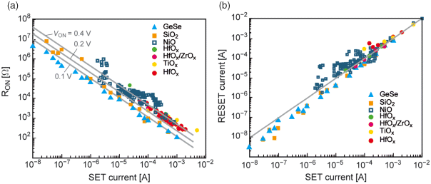
Figure 8.4 (a) ON resistance RON as a function of SET current compliance current for various material systems. (b) RESET current (maximum current before OFF switching) as a function of SET current compliance current for various material systems. Reproduced with permission from [9], © 2012 Wiley-VCH
It is experimentally observed that the RESET current scales linearly with the programming SET current (cf. Figure 8.4b). This empirical relation can be explained by the nonlinear switching kinetics and the almost linear I-V characteristic in the ON state. The RESET driving force is strongly voltage-dependent and almost independent of the programmed ON state. This results in a nearly constant RESET voltage VRES for a distinct ReRAM under the same external switching conditions. In combination with the linear ON state we can write
Here, A is a system inherent constant. It should be noted that these empirical laws are independent of the actual switching mechanism as long as the system exhibits nonlinear switching kinetics. It has been shown by simulation that a thermally assisted lateral growth of a low resistive filament as well as the electrochemical change of a tunneling gap leads to these empirical generic switching characteristics.
8.2.5 Modeling Redox Memories for Circuit Simulations
The basic requirement for a behavioral model is to reproduce the device properties for arbitrary excitation signals and connection to further electronic components, for example, series resistors or further devices. Having this requirement in mind we review existing approaches and try to categorize them.
8.2.5.1 Quasi-Static Models
Quasi-static models have been the basic approach to model ReRAMs cells [10] and are extracted from quasi-static I-V characteristics. The advantage of this approach is the direct accessibility from measurement data which can directly fitted to obtain a usable model. The limitations of this approach directly result from absence of sweep rate/pulse rate dependency and the unfeasibility of any gradual multilevel properties.
8.2.5.2 Initial Dynamical Models
The development of dynamical models has obeyed a great advance by the initial memristive device model of Strukov et al. [11]. In this approach, the device is considered a dynamical system offering a readout and state equation of the form [12]:
or
The relevance of a certain dynamical model depends strongly on the applied differential equation, that is, the detailed understanding of the device physics. Starting from the basic linear model [11], several kinds of window functions were applied to enter more physical behavior to the model, for example [13–15]. But, this approach is limited since actual device properties cannot be modeled accurately.
8.2.5.3 Empirical Dynamical Models
In a next step, the concepts of the dynamical model were applied to specific devices and their dynamical behavior. In this approach, generic nonlinear equations (e.g., sinh equations) as well as certain physics-based equations (e.g., tunneling equations) are used to build-up dynamical models whose parameters are fitted to the experimental data, for example [16,17].
8.2.5.4 Generic Physics-based Dynamical Models
In this approach physical considerations are the starting point for modeling rather than experimental observations, leading to models for generic device classes, for example, ECM or VCM cells. In deference to the empirical approach, the physics-based approach tries to implement the internal physics as accurately as possible, avoiding piecewise definitions among others. For example, the fact that a ReRAM cell is mixed-ionic-electronic models – thus offer at least two current paths – is considered in this approach, see for example [18].
Sections 8.3 and 8.4 discuss selected empirical as well as generic physics-based modeling approaches for ECM and VCM cells, respectively.
8.3 Electrochemical Metallization Memory Cells
Electrochemical metallization memory (ECM) cells, also known as programmable metallization memory cell (PMC), conductive bridge random access memory (CBRAM) or atomic switch, rely on the electrochemical growth and dissolution of a conducting filament within the insulating layer [19,20]. They consist of an active Cu or Ag electrode, a cation conducting insulating layer, and an inert counter electrode such as Pt, W, or Ir [21]. The ECM effect has been demonstrated in typical insulators such as Ta2O5 [22], TiO2 [23], HfO2 [24], or SiO2 [25] as well as solid electrolytes (e.g., AgI [26], GeS [27]). ECM cells exhibit multibit data storage capability [28], scalability almost down to the atomic level [29], and very low programming power [2]. Moreover, potential back end of line (BEOL) compatible integration has been demonstrated [30] making ECM cells of high interest for future nonvolatile memory.
8.3.1 Physical Switching Mechanism
8.3.1.1 Electroforming and SET Process
The electroforming and the SET process in ECM cells involve the same electrochemical steps as illustrated in Figure 8.5.
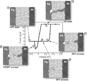
Figure 8.5 A typical quasi-static I-V characteristic of an ECM cell, here Ag/Ag-Ge-Se/Pt. The ON resistance is determined by the SET current compliance. The insets A to E show the different process steps: Step A – OFF state, steps B, C – SET process, step D – ON state, step E – RESET process. Reproduced with permission from [9], © 2012 Wiley-VCH
When a positive voltage is applied to the Cu or Ag active electrode, that electrode is oxidized electrochemically by a charge transfer process. The corresponding cation is dissolved into the insulating layer and migrates under the applied electric field towards the inert cathode (step B). At the cathode a redox reaction takes place and the cations are reduced. After formation of a stable nucleus a metallic Cu or Ag filament starts to grow towards the active electrode (step C). As the filament approaches the anode an electron tunneling current sets in and finally the preset current compliance is reached (step D). Any further resistance change forces the voltage to decrease and further filamentary growth is suppressed [18]. The formation of the metallic filament is accompanied with mechanical stress. Hence, a prerequisite for proper ECM operation is supposed to be the existence of extended defects such as nanopores or grain boundaries within the insulating layer. As illustrated in Figure 8.6a, the initial switching voltage during the electroforming cycle is higher than in the successive switching cycles [25].
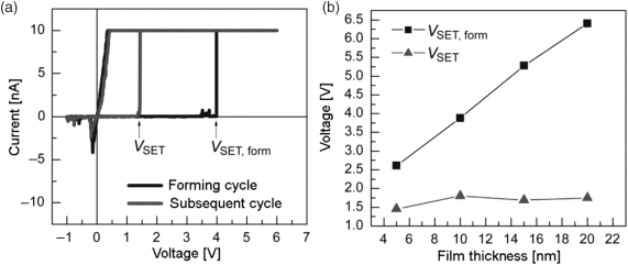
Figure 8.6 (a) Depending on the actual material system, in the initial forming cycle much larger voltages than the subsequent cycles are required, as shown here for Cu/SiO2/Pt. (b) The initial SET forming voltage shows a clear thickness dependency while the subsequent SET voltages show no SiO2 film thickness dependency. Reprinted with permission from [25]. Copyright 2009, American Institute of Physics
Moreover, the switching voltage during the electroforming cycle is thickness-dependent, whereas it is almost thickness independent for all following cycles. Probably, the formation of the filament during the initial cycles involves mechanical stress, which makes the filamentary growth the limiting process. After RESET a template for fast ionic transport has been formed leading to the almost constant switching voltage.
The strength of the electric contact is determined by the preset current compliance level during the SET process according to RON ∝ Icc−1. In this way the ON resistance can be adjusted over 10 orders of magnitude (see Figure 8.4).
The origin of the multilevel states has been attributed to varying tunneling gaps between the active electrode and the growing filament for ON resistances higher than RON > 12.9 kΩ [18]. This resistance value corresponds to a single atomic contact conductance, that is, 1/G0 = 12.9 kΩ [31]. In this resistance regime quantized conduction steps have been observed [22,26,32] as illustrated in Figure 8.7.
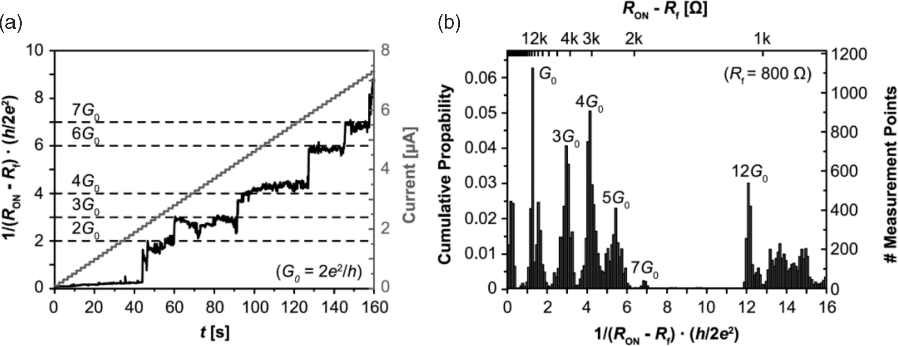
Figure 8.7 (a) In ECM (here: AgI-based) cells, single atomic contacts can occur, leading to quantized conductance offering conductance which is a multiple of G0. (b) Cumulative statistics of the ECM cell conductivity. Reproduced with permission from [26], © 2012 IOP
This gives an indirect proof of the existence of a remaining tunneling gap for RON > 1/G0. Below this boundary the on resistance decreases further first by quantized steps and then more continuous by filament widening. This filament widening can be very small since the filament resistivity is diameter dependent according to Fuchs–Sondheimer theory [33]. Note that a further lateral growth is accompanied by mechanical stress.
ECM cells show strongly nonlinear switching kinetics. Based on the switching mechanism each physical process can be the rate limiting step. Depending on the materials involved and thermodynamic conditions, this can be: (i) the nucleation process prior to filamentary growth, (ii) the electron-transfer reaction occurring at the metal/insulator interfaces, and (iii) the ion transport within the electrolyte/insulator thin film (cf. Equations 8.1–8.3) [26,34,35]. Figure 8.8 shows the SET switching kinetics for a AgI system, which exhibits three distinct regimes [35]. By comparison to a simulation model these regime could be identified as (i) nucleation limited regime, (ii) electron transfer limited regime, and (iii) limitation by electron transfer and ion transport.

Figure 8.8 SET time as a function of pulse height for AgI-based cells. The symbols denote the experimental data and the solid lines simulation results. Reproduced by permission of the PCCP Owner Societies [35]
This demonstrates that the rate-limiting process also depends on the voltage regime. Due to the low currents involved during SET switching a temperature enhancement of the switching kinetics is rather unlikely.
8.3.1.2 RESET Process
The RESET mechanism strongly depends on the type of ON state. As previously discussed a tunneling gap can remain for low current compliances, whereas a true galvanic contact is achieved for high current compliances. In the former case the electrochemical cell is still present and the RESET is simply achieved by applying a negative potential to the active electrode [18]. The cell operation is inherently bipolar. If a galvanic contact is established during SET operation the conducting filament bridges the two metal electrodes. Due to the low ON resistance Joule heating will occur at the narrowest part of the filament [36,37]. Here, surface tension at the metal surface (temperature assisted ad-atom diffusion leading to Ostwald ripening) may contribute to the rupture. Due to temperature increase the electron transfer reactions occurring at the boundary are thermally enhanced (cf. Equation 8.2). This leads to a self-dissolution of the filament, that is, oxidation and reduction occur at the filament rather than at the filament and the active electrode [38]. After filament rupture the electrochemical RESET further proceeds as in the remaining tunneling gap case. Due to the self-dissolution of the bridging filament and the thermal nature of the RESET, the RESET process can be polarity-independent as reported in experiment [38].
The RESET switching kinetics have been rarely investigated. According to the study of Kozicki et al. the RESET time is a function of the ON state resistance and is also strongly voltage dependent [36]. Here, the ON resistance is very low suggesting a galvanic contact. In this regime first a lateral dissolution has to occur, which might explain the dependence of the RESET time on the ON state. For higher resistance state corresponding to a remaining tunneling gap in ON state, the RESET time is presumably independent on the ON resistance. In contrast to the SET switching kinetics the limiting factors are only the electron transfer reaction and the ionic transport, whereas a nucleation process does not occur. If a galvanic contact is present, the RESET switching is also thermally enhanced.
8.3.2 Modeling
Several compact behavioral models for ECM cells have been published. Basically, two different approaches have been pursued: (i) vertical [18,39,40] and (ii) lateral filamentary growth [28,36,41]. For the first approach the filament length or the tunneling gap between growing filament tip and counter electrodes are used as state variable, whereas in the latter the state variable is the filament radius.
A first self-consistent model for vertical filamentary growth has been published by Menzel et al. [42], which has been later extended to multilevel switching [18] and to model the SET switching kinetics including all relevant processes [35]. The dynamic state equation describing the tunneling gap x is given by Faradays law
where k is a constant. The equivalent circuit diagram is shown in Figure 8.9a. Note that the change in the state variable only depends on the ionic current and not the electronic current as in the standard memristor-like models (cf. Section 8.2.5). The model accounts for the nonlinear switching kinetics, I-V characteristics, and the multilevel switching by modulation of the tunneling gap (see Figure 8.9b,c).
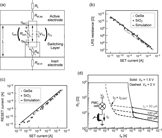
Figure 8.9 (a) Equivalent circuit model of ECM cell. Note the two current paths, one for the ionic and one for the electronic current. Reprinted with permission from [18]. Copyright 2012, American Institute of Physics. (b,c) The vertical ECM model accounts for nonlinear switching kinetics and reproduces experimental findings of SET current compliance dependencies for RESET current and actual LRS resistance. Reprinted with permission from [18]. Copyright 2012, American Institute of Physics. (d) In a 1T1R structure, the drain current ID limits the maximum device current, thus plays the role of a current compliance. Depending on ID a certain resistance level can be written. © 2009 IEEE. Reprinted, with permission, from [28]
The change of the filament diameter was first used to model the RESET in ECM cell by Russo et al., and was supplemented by the SET modeling later [28,36] (see Figure 8.9d). This model has been also adapted by Yu et al. [41]. In this model Joule heating is also included due to the high currents involved. The state equation for radial dissolution and growth reads
where k is a constant. Also in this model the state equation depends only on the ionic current. Note that the algebraic sign in Equation 8.9 has to be changed for SET and RESET and the dynamic state equations are not self-consistent as in the vertical model. The lateral growth model has been used to describe multilevel switching and the switching kinetics. According to the considerations in the previous section the lateral growth model is restricted to the small resistance regime in which the filament bridges both electrodes, whereas the vertical growth model is valid until a galvanic contact is established. Both models could be thus easily combined. The occurrence of quantized conduction steps, however, is not covered by either model.
8.4 Valence Change Memory Cells
In valence change memory (VCM) cells the resistive switching effect relies on the motion of oxygen vacancies (respectively oxygen ions) and a subsequent redox reaction on the nanoscale. This leads to a valence change of the cation sublattice, which in turn changes the local conductivity. Due to the involved ion migration the device operation is inherently bipolar. The VCM effect has been observed in binary oxides as well as perovskites, where the insulating layer is a mixed ionic electronic conductor. Typically, the MIEC is sandwiched between an Ohmic electrode (OE) and an active electrode (AE) consisting of a high work function/less oxygen affinity metal [43]. Typically, the resistive switching takes place in front of the latter electrode. Many variants of VCM switching are known such as filamentary- or interface-type switching or in p- or n-conducting MIEC oxides. Here, we will focus on the filamentary type switching in n-conducting MIEC oxide, which is the common type of VCM switching. VCM cells represent a highly promising NVM technology because of its recent performance demonstrations: for example, very high endurance (>1012 [44]), ultrafast switching (<1 ns [45]), high scalability (down to <10 nm [46]), and low power operation (<0.1 pJ [47]). In addition, multiple resistance states in a single ReRAM cell can be achieved by proper programming [48,49].
8.4.1 Physical Switching Mechanism
8.4.1.1 Electroforming Process
In general, an initial electroforming process is required prior in order to switch the MIM cell repetitively. The electroforming voltage is significantly higher than the SET/RESET voltage in the following switching cycles. Depending on the MIM stack an electroforming into the LRS as well as the HRS is possible, whereas the former is the more common process. In a MIM cell with identical metal electrodes the electroforming process induces an asymmetry and defines active and ohmic electrodes. During the electroforming process the oxide material is reduced and the MIM stack becomes conducting. Typically, this process is nonuniform and leads to the formation of n-conducting filaments or even induces a phase transformation, for example, a Magnéli phase Ti4O7 in TiO2-based VCM cells [50]. Due to the localized currents and the relatively high voltages very high local temperatures are achieved, which accelerates the forming process. The microscopic mechanism is described using the process of forming the HRS as an example. Let us consider a cell with one low work function metal electrode, for example, Ti, and one high work function metal electrode such as Pt. By application of a positive potential to the active electrode oxygen is released at the anode leaving oxygen vacancies behind. The positively charged oxygen vacancies migrate under the applied electric field towards the cathode. They pile up at the cathode increasing locally the conductivity and the electric field in this region is reduced. Subsequently, a virtual cathode grows towards the anode until the current compliance is reached [3,51].
Alternatively, the forming process in HfOx-based VCM cells has been described in terms of moving oxygen interstitials [52]. In contrast the oxygen vacancies are assumed to be immobile and to serve as deep trap states facilitating trap assisted tunneling current. Due to the applied electric field and local Joule heating this model suggests that the Hf–O bond breaks and an oxygen vacancy is created. The interstitial oxygen vacancy diffuses away from the vacancy and avoids recombination. These additional oxygen vacancies increase the trap assisted tunneling current and a self-accelerating process sets in leading to the formation of a highly reduced filament. Many aspects within this model remain unresolved at the current state of knowledge.
The electroforming voltage depends on the MIEC thickness. As a consequence, forming-free MIM cells can be fabricated using very thin oxide films (2–3 nm) [53]. By building in oxygen gradients during deposition of the oxide film (e.g., by deposition of bilayer structures such as TiOx/TaOx [54]), the electroforming voltages might be reduced. For WOx-based VCM cell it is reported that the as-deposited film is highly deficient of oxygen and thus highly conducting [55]. Hence, the resistance needs to be increased during electroforming to allow resistive switching.
8.4.1.2 SET and RESET
Figure 8.10 illustrates a typically filamentary SET and RESET mechanism in VCM cells.
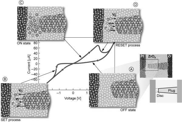
Figure 8.10 Typical I-V characteristic of a VCM cell. Pt is the active electrode of the Pt/ZrOx/Zr stack while Zr is a purely ohmic contact. Light gray spheres indicate oxygen vacancies while dark spheres stand for lower-valence Zr ions. Note: only oxygen vacancies are mobile! The steps A to D show the switching process: step A – OFF state, step B – SET process, step C – ON state, step D – RESET process. Reproduced with permission from [9], © 2012 Wiley-VCH
In this model, the HRS conducting filamentary region consists of a highly oxygen-deficient region and an oxygen-rich region near the active electrode. The corresponding band diagram exhibits an electrostatic barrier which defines the electric current. This band diagram facilitates an asymmetric I-V characteristic. By application of a negative potential to the active electrode the oxygen vacancies move towards the active electrode. A local redox reaction (i.e., the reduction of Zr ions in the disc; cf. Figure 8.10) occurs and the local conductivity is increased. This means that the barrier height and width are reduced enabling high tunneling currents and the cell switches to the LRS. Eventually, the electron barrier conduction is increased so much that the cell exhibits a linear, that is, a metal-like I-V characteristic. By reversing the polarity the oxygen vacancies are pushed backed and the HRS is re-established. In the picture of moving interstitial oxygen ions the switching polarity is the same. To enable RESET switching the oxygen ions have to recombine with the oxygen vacancies and the SET process is equivalent to the described electroforming process [6,52,56]. The above described switching polarity is called counter-eight-wise. In contrast, the switching polarity is called eightwise when the switching occurs at the same electrode but with opposite polarities for SET and RESET.
Resistive switching with both polarities has been experimentally observed. It can also occur in the same device by proper electrical stimuli [43,53]. This behavior can be attributed, for example, to the change of the active switching interface [43], which means it is still counter-eight-wise switching. In contrast the counter-eightwise switching in SrTiO3-based VCM cells has been attributed to a filamentary switching mechanism, while the eightwise switching occurs on a larger area at the same electrode [57]. Ultimately, complementary switching within a cell can occur, where the two different interfaces correspond to the two anti-serially connected bipolar switches of complementary resistive switch [58].
VCM cells show highly nonlinear SET and RESET switching kinetics. Here, the ion migration is supposed to be the limiting step due to the very low mobility of oxygen vacancies at room temperature and low electric fields. According to the Mott–Gurney law of ion hopping (cf. Equation 8.1) the ion transport can be either field or temperature enhanced. Due to the high current densities, involved in VCM switching, Joule heating is expected. The exact balance between these two effects depends on the specific MIM cell and the considered voltage regime. For very fast switching high currents and voltages are involved, supposing temperature as the dominating factor. During quasi-static switching very low programming power has been observed indicating that the electric field may be the dominating factor in this regime.
8.4.2 Modeling
In this section, typical dynamical models for VCM devices are highlighted. We restrict our considerations to models which are written as a dynamical system or at least can simply be rewritten in this manner (compare Equations 8.6 and 8.7).
First, we want to mention the TaOx-VCM model presented by Hur et al. [59]. This model is based on the work of Strukov et al. [11] and keeps the linear dependency of R on the state variable x which corresponds to the length of a low resistive domain (i.e., a vertical filament) w here
To model physical boundary conditions a window function is applied for calculation of the state variable
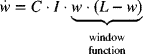
Furthermore, the model accounts for the active electrode by introducing a Schottky barrier and includes field induced barrier lowering. The equivalent circuit model is depicted in Figure 8.11a and the simulation results in Figure 8.11b. The model is able to reproduce quasi-static I-V characteristics very well, but due to lack of nonlinearity in the state variable, dynamic properties of fast pulses for example will not be feasible by this model. Furthermore, as in the basic memristor models [14,15] the physical plausibility of the window function is only weak.
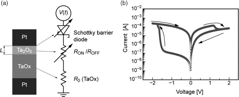
Figure 8.11 (a) Equivalent circuit model of a TaOx VCM-type cell. (b) Simulated I-V curve which fits well to experimental data. Reprinted figure with permission from [59]. Copyright (2010) by the American Physical Society
Next, we consider the TiOx model from Pickett [16,60], another further development of the initial “memristor” model [11]. The basic modeling idea is depicted in Figure 8.12a showing a conductive channel which is modeled as a series resistor Rs and a gap which is described by a tunneling equation, and the state variable x which is considered the tunneling barrier width w. The advantages of this model are the nonlinear dependency on the state variable (tunneling equation) and the avoidance of an explicit window function. Hence, the model is physically motivated, but the total approach is still mainly empirical, trying to fit simulations to an experimental quasi-static I-V curve (Figure 8.12b). Furthermore, the existence of two current paths – one electronic and one ionic – is not reflected by this model at all.
Figure 8.12 (a) Equivalent circuit model of a TiOx VCM-type cell. (b) Measured I-V and fitted simulation curve. © 2011 IEEE. Reprinted, with permission, from [60]
For VCM cells, there are also models assuming a lateral growth of a filament [61], thus the state variable x corresponds to the diameter of the filament. Furthermore, temperature could be implemented as an additional state variable, too.
In [62], the importance of the temperature as an additional state variable is highlighted. Here, a typical VCM cell (Ti/SrTiO3/STO:Nb) is considered, which consists of an active Ti electrode, an ohmic STO:Nb bottom electrode, a highly conducting plug (created during electroforming) and a disc region where the switching takes place (see Figure 8.13a). Since the kinetics of the switching are determined by the drift velocity of the oxygen vacancies, both temperature and E-field acceleration could have significant impact. However, from the simulations in [62], the major contribution is due to temperature acceleration (see Figure 8.13b), making temperature one of the most important internal state variables, and thus should be considered in accurate VCM modeling.
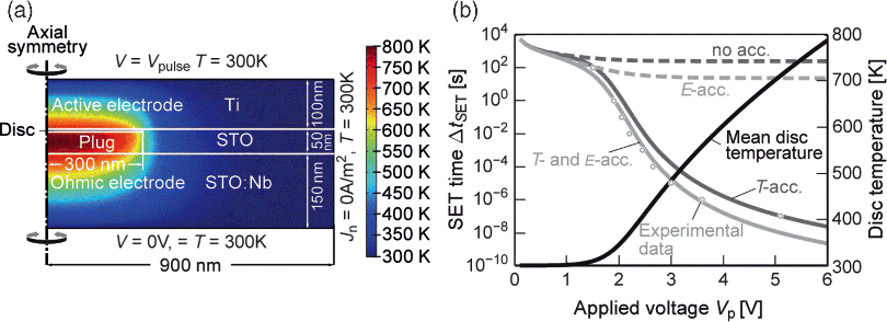
Figure 8.13 (a) Cross-section of a SrTiO3 VCM cell using finite element (FEM) simulations. For a 5 V voltage pulse, the active disc region heats up to 800 K. (b) The SET time as a function of the applied pulse height. To fit the experimental data, strong temperature acceleration is needed. Pure field acceleration is not sufficient to explain the observed experimental nonlinear SET kinetics. Reproduced with permission from [62], © 2011 Wiley-VCH
In general, the challenge for VCM device modeling is the lack of detailed physical understanding of these devices, which makes physics-based modeling so difficult. Thus, in contrast to ECM modeling no generic physics-based dynamical models is available for VCM cells so far.
8.5 Performance
There are several metrics which can be applied to evaluate the performance of emerging memory devices [1]. Here we will present the most relevant criterions and corresponding best results from literature.
8.5.1 Minimum Feature Size
In terms of scalability the minimum feature size is the most significant figure of merit. In theory, feature sizes down to F = 4 nm are projected [63], and features sizes of F =30 nm [44] or even F = 10 nm [46] have been shown for experimental setups for VCM cells (compare Figure 8.14). For ECM cells feature sizes down to 20 nm have been reported on [64,65]. Ultimatively, ECM operation has been demonstrated with only a few atoms involved [29].
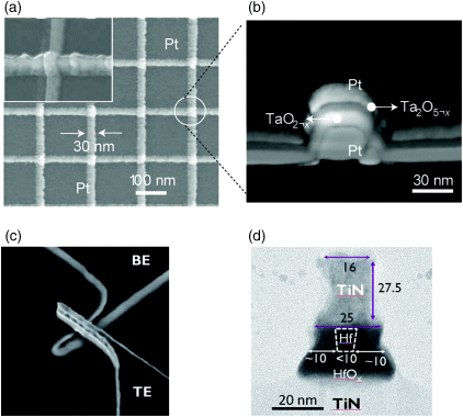
Figure 8.14 (a,b) A feature size of F = 30 nm were reported on for TaOx VCM devices in a crossbar array by Lee et al. [44]. Reprinted by permission from Macmillan Publishers Ltd: Nature Materials [44], copyright (2011). (c,d) Single crosspoint structures down to F = 10 nm were shown for HfOx-based VCM devices. © 2011 IEEE. Reprinted, with permission, from [46]
8.5.2 Minimum Cell Area
The minimum cell array is highly relevant for area efficient memory layout. Due to the two-terminal nature of ReRAM devices the minimum cell area within crossbar arrays, which is 4F2, is feasible (Figure 8.15a). By applying 3D stacking techniques, for 1R, 1D1R or 1CRS devices even 4F2/n can be achieved (Figure 8.15b), where n is the number of stacked layers, in a crossbar array configuration.
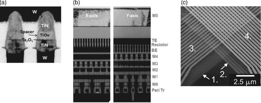
Figure 8.15 (a,b) A fully integrated TiOx/Ta2O5-based crossbar array was presented in [66]. © 2012 IEEE. Reprinted, with permission, from [66]. (c) The feasibility of 3D stacking for crossbar arrays (here four layers) is depicted on the SEM picture (half pitch 200 nm). © 2009 IEEE. Reprinted, with permission, from [67]
In principle, the scaling of ReRAM cells can be driven into the few nanometer range. For VCM cells, the redox-based resistive switching has been demonstrated at the exits of dislocations of SrTiO3 single crystals with a lateral extension of less than 2 nm [68]. For ECM cells, the atomic switch concept with the Landauer conductance steps indicates contacts of few metal atoms [69]. Figure 8.15a shows a VCM device (TiOx/Ta2O5) while Figure 8.15b shows a ECM array (Ag-MSQ).
8.5.3 Minimum Switching Time
The minimum switching time is directly related to the nonlinear device kinetics described above; compare also [62]. In [70], fast pulse analysis of TiOx VCM nano-crossbars revealed (Figure 8.16a) feasible operation speed of<5 ns. In [45] an experimental coplanar waveguide test setup was used to demonstrate even faster switching properties of VCM-type TaOx ReRAM cells (picoseconds), see Figure 8.16b. For ECM devices no coplanar waveguide test setup measurements were performed yet, and minimum observed switching is below 10 ns [71].
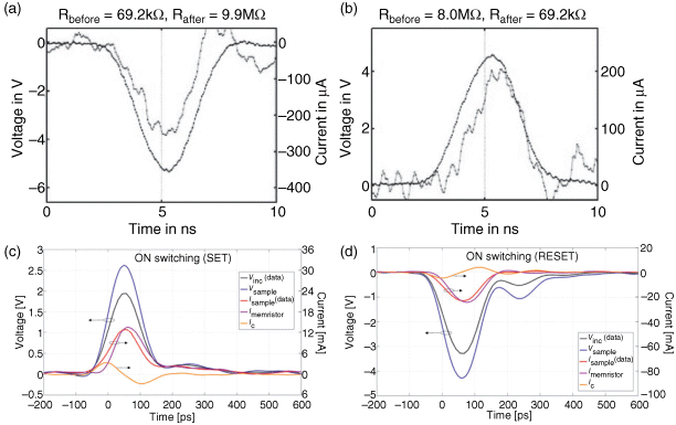
Figure 8.16 (a, b) Fast switching in TiO2-based VCM cells. © 2011 IEEE. Reprinted, with permission, from [70]. (c, d) Sub-nanosecond ON and OFF switching could be shown for TaOx VCM cells. Reproduced with permission from [45], © 2011 IOP
8.5.4 Retention Time
Data retention is another important issue for memories. Using elevated temperature experiments, the time to fail can be estimated (compare Figure 8.17). VCM-type TaOx-based ReRAM cells were investigated and the time to fail for the tail bits of a 256 kbit array (1T1R) was estimated to be larger than 10 years at 85 °C [72] (Figure 8.17a). For Ag-chalcogenide ECM cells retention times larger 10 years were also estimated (Figure 8.17b).
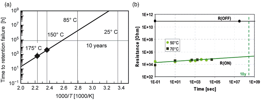
Figure 8.17 (a) Arrhenius plot visualizing the retention behavior at elevated temperatures and the extrapolated trend for lower temperatures. © 2012 IEEE. Reprinted, with permission, from [72]. (b) Increase in ON-state resistance with time. The retention is extrapolated. © 2005 IEEE. Reprinted, with permission, from [64]
8.5.5 Write Cycles
Besides retention, the maximum number of write cycles is important for the feasibility of long-life memories. Up to 1012 write cycles subsequent RESET-read-SET-Read-cycles could be performed for TaOx-based VCM cells (see Figure 8.18a). For Ag-GeSe ECM devices 1010 write cycles are feasible (see Figure 8.18b). Especially, the endurance data for TaOx-based VCM cells is very promising and can be considered a milestone on the way to future ReRAM memories.
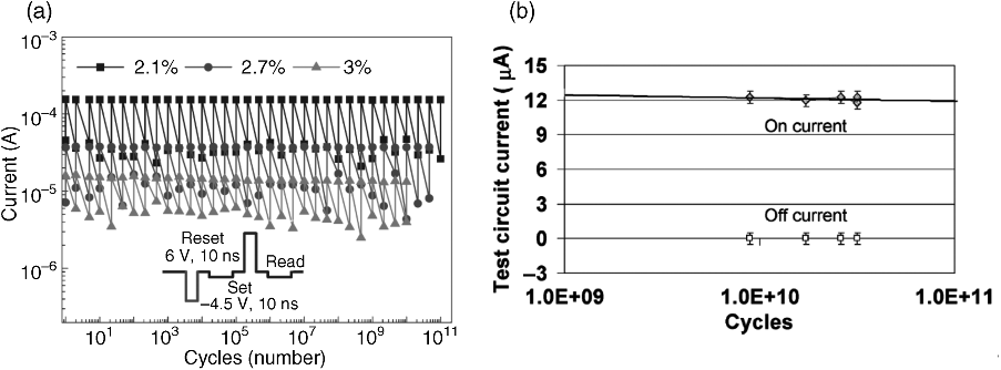
Figure 8.18 (a) TaOx VCM devices offer promising endurance properties. Up to 1012 write cycles could be shown in [44]. Best results were obtained with an oxygen content of 3%. Reprinted by permission from Macmillan Publishers Ltd: Nature Materials [44], copyright (2011). (b) Ag-GeSe ECM devices offer endurance of 1010 write cycles. © 2005 IEEE. Reprinted, with permission, from [73]
8.5.6 Multilevel
To compete with FLASH memories multiple bits should be stored in each ReRAM cell. For both VCM as well as ECM cells, multi-bit properties could be shown (see Figure 8.19).
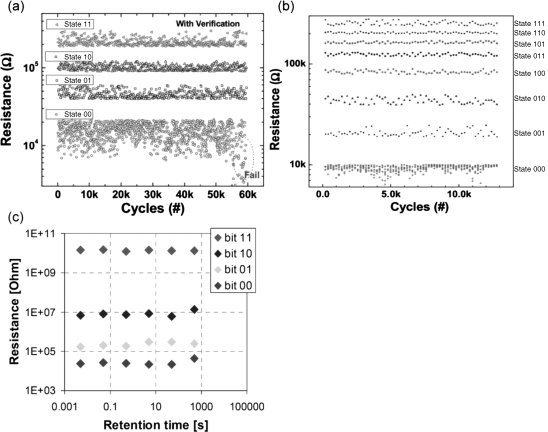
Figure 8.19 (a,b) WOx-based VCM cells offering multilevel properties, either two bit (a) or even three bit (b). A read–verify technique was applied. © 2011 IEEE. Reprinted, with permission, from [49]. (c) Ag-based ECM cells showing two-bit multilevel behavior. © 2007 IEEE. Reprinted, with permission, from [complete publication information]
In [49] two bits (Figure 8.19a) and up to three bits per cell (Figure 8.19b) were feasible (VCM), while in [74] two bits per cell (ECM) could be stored. The results are summarized in Table 8.1.
Table 8.1 Multi-bit properties of ReRAM cells
| Performance | Best value | Material system | References | |||
| measure | VCM | ECM | VCM | ECM | VCM | ECM |
| Minimum feature size F | 10 nm | <10 nm | HfOx | Ag-chalcogenide | [46] | [29,64] |
| Minimum cell area | 4F2 | 4F2 | Any | Any | See, for example, [66] | See, for example, [75] |
| Minimum switching time | < 200 ps | <10 ns | TaOx | Ag-MSQ | [45] | [71] |
| Retention time | >10 yr (extrapolated) | >10 yr (extrapolated) | TaOx | Ag-chalcogenide | See, for example, [72] | [64] |
| Write cycles | >1012 | >1010 | TaOx | Ag-GeSe | [44] | [73] |
| Multilevels | 8 | 4 | WOx | Ag-chalcogenide | [49] | [74] |
8.6 Summary
Redox-based resistive nonvolatile memories are among the most promising emerging memory devices. The devices can be classified by means of the mechanisms either as ECM, VCM or TCM. Both ECM and VCM devices offer the good properties for future memory applications, while ECM cells are much better understood than VCM devices. This issue is reflected in the availability of physics-based device models which are much more elaborated for ECM cells.
For modeling, the fact that ReRAMs are MIEC devices must be taken into account, thus models should offer at least two current paths. Moreover window functions should be used with caution, since the physical accuracy is often low. To model a restricted device domain, for example, the quasi-static behavior, this approach may be valid, but one should be aware of the limitation. A good first check for device model consistency is if the device models can reproduce the frequency dependency of tSET/tRESET as well as the multilevel behavior, that is, offer the correct inherent nonlinear switching kinetics.
In terms of actual device performance one can say that VCM cells in general offer more stable mode of operation, while ECM cells are more power-efficient. Both types of cells show excellent scaling potential, and in combination with a suitable selector, large-scale 4F2 structures are feasible.
References
- 1. ITRS (2011). “The International Technology Roadmap for Semiconductors - ITRS 2011 Edition”.
- 2. Waser, R. and Aono, M. (2007) Nanoionics-based aresistive switching memories. Nature Materials, 6, 833–840.
- 3. Waser, R., Dittmann, R., Staikov, G., and Szot, K. (2009) Redox-based resistive switching memories - nanoionic mechanisms, prospects, and challenges. Advanced Materials, 21, 2632–2663.
- 4. Tappertzhofen, S., Menzel, S., Valov, I., and Waser, R. (2011) Redox processes in silicon dioxide thin films using copper microelectrodes. Applied Physics Letters, 99, 203103.
- 5. Goldfarb, I., Miao, F., Yang, J.J. et al. (2012) Electronic structure and transport measurements of amorphous transition-metal oxides: observation of Fermi glass behavior. Applied Physics A-Materials Science & Processing, 107, 1–11.
- 6. Wong, H.-S.P., Lee, H.-Y., Yu, S. et al. (2012) Metal–Oxide RRAM. Proceedings of the IEEE, 100, 1951–1970.
- 7. Meuffels, P. and Schröeder, H. (2011) Comment on Exponential ionic drift: fast switching and low volatility of thin-film memristors by D.B. Strukov and R.S. Williams in Applied Physics A, 94, 515–519 (2009). Applied Physics A: Materials Science and Processing, 105, 65–67.
- 8. Szot, K., Rogala, M., Speier, W. et al. (2011) TiO2 – a prototypical memristive material. Nanotechnology, 22, 254001/1–254001/21.
- 9. Waser, R., Menzel, S., and Bruchhaus, R. (2012) Nanoelectronics and Information Technology, 3rd edn, Wiley-VCH.
- 10. Mustafa, J. and Waser, R. (2006) A novel reference scheme for reading passive resistive crossbar memories. IEEE Transactions on Nanotechnology, 5, 687–691.
- 11. Strukov, D.B., Snider, G.S., Stewart, D.R., and Williams, R.S. (2008) The missing memristor found. Nature, 453, 80–83.
- 12. Chua, L.O. and Kang, S.M. (1976) Memristive devices and systems. Proceedings of the IEEE, 64, 209–223.
- 13. Joglekar, Y.N. and Wolf, S.J. (2009) The elusive memristor: properties of basic electrical circuits. European Journal of Physics, 30, 661–675.
- 14. Biolek, Z., Biolek, D., and Biolkova, V. (2009) SPICE model of memristor with nonlinear dopant drift. Radioengineering, 18, 210–214.
- 15. Benderli, S. and Wey, T.A. (2009) On SPICE macromodelling of TiO2 memristors. Electronics Letters, 45, 377–379.
- 16. Pickett, M.D., Strukov, D.B., Borghetti, J.L. et al. (2009) Switching dynamics in titanium dioxide memristive devices. Journal of Applied Physics, 106, 074508.
- 17. Sheridan, P., Kim, K.H., Gaba, S. et al. (2011) Device and SPICE modeling of RRAM devices. Nanoscale, 3, 3833–3840.
- 18. Menzel, S., Böttger, U., and Waser, R. (2012) Simulation of multilevel switching in electrochemical metallization memory cells. Journal of Applied Physics, 111, 014501.
- 19. Valov, I., Waser, R., Jameson, J.R., and Kozicki, M.N. (2011) Electrochemical metallization memories-fundamentals, applications, prospects. Nanotechnology, 22, 254003.
- 20. Hasegawa, T., Terabe, K., Tsuruoka, T., and Aono, M. (2012) Atomic switch: Atom/ion movement controlled devices for beyond von-neumann computers. Advanced Materials, 24, 252–267.
- 21. Valov, I. and Kozicki, M.N. (2013) Cation-based resistance change memory. Journal of Physics D: Applied Physics, 46, 074005.
- 22. Tsuruoka, T., Hasegawa, T., Terabe, K., and Aono, M. (2012) Conductance quantization and synaptic behavior in a Ta2O5-based atomic switch. Nanotechnology, 23, 435705.
- 23. Yang, L., Kügeler, C., Szot, K. et al. (2009) The influence of copper top electrodes on the resistive switching effect in TiO2 thin films studied by conductive atomic force microscopy. Applied Physics Letters, 95, 13109.
- 24. Wang, Y., Liu, Q., Long, S. et al. (2010) Investigation of resistive switching in Cu-doped HfO2 thin film for multilevel non-volatile memory applications. Nanotechnology, 21, 245202.
- 25. Schindler, C., Staikov, G., and Waser, R. (2009) Electrode kinetics of Cu-SiO2-based resistive switching cells: Overcoming the voltage-time dilemma of electrochemical metallization memories. Applied Physics Letters, 94, 072109.
- 26. Tappertzhofen, S., Valov, I., and Waser, R. (2012) Quantum conductance and switching kinetics of AgI based microcrossbar cells. Nanotechnology, 23, 145703.
- 27. Kozicki, M.N., Balakrishnan, M., Gopalan, C. et al. (2005) Programmable metallization cell memory based on Ag-Ge-S and Cu-Ge-S solid electrolytes. Proceedings of the Non-Volatile Memory Technology Symposium (NVMTS), 20, 83–89.
- 28. Russo, U., Kamalanathan, D., Ielmini, D. et al. (2009) Study of multilevel programming in programmable metallization cell (PMC) memory. IEEE Trans Electron Devices, 56, 1040–1047.
- 29. Terabe, K., Hasegawa, T., Nakayama, T., and Aono, M. (2005) Quantized conductance atomic switch. Nature, 433, 47–50.
- 30. Bernard, Y., Renard, V.T., Gonon, P., and Jousseaume, V. (2011) Back-end-of-line compatible conductive bridging RAM based on Cu and SiO2. Microelectronic Engineering, 88, 814–816.
- 31. Scheer, E., Agrait, N., Cuevas, J. et al. (1998) The signature of chemical valence in the electrical conduction through a single-atom contact. Nature, 394, 154–157.
- 32. Jameson, J.R., Gilbert, N., Koushan, F. et al. (2012) Quantized conductance in Ag/GeS2/W conductive-bridge memory cells. IEEE Electron Device Letters, 33, 257–259.
- 33. Sondheimer, E.H. (1952) The mean free path of electrons in metals. Advances in Physics, 1, 1–42.
- 34. Valov, I., Sapezanskaia, I., Nayak, A. et al. (2012) Atomically controlled electrochemical nucleation at superionic solid electrolyte surfaces. Nature Materials, 11, 530–535.
- 35. Menzel, S., Tappertzhofen, S., Waser, R., and Valov, I. (2013) Switching kinetics of electrochemical metallization memory cells. PCCP, 15, 6945–6952.
- 36. Kamalanathan, D., Russo, U., Ielmini, D., and Kozicki, M.N. (2009) Voltage-driven on-off transition and tradeoff with program and erase current in programmable metallization cell (PMC) memory. IEEE Electron Device Letters, 30, 553–555.
- 37. Tsuruoka, T., Terabe, K., Hasegawa, T., and Aono, M. (2010) Forming and switching mechanisms of a cation-migration-based oxide resistive memory. Nanotechnology, 21, 425205.
- 38. Menzel, S., Adler, N., van den Hurk, J. et al. (2013) Simulation of polarity independent RESET in electrochemical metallization memory cells, Proceedings of the 5th IEEE International Memory Workshop (IMW).
- 39. Jameson, J.R., Gilbert, N., Koushan, F. et al. (2011) One-dimensional model of the programming kinetics of conductive-bridge memory cells. Applied Physics Letters, 99, 063506.
- 40. Lin, S., Zhao, L., Zhang, J. et al. (2012) Electrochemical Simulation of Filament Growth and Dissolution in Conductive-Bridging RAM (CBRAM) with Cylindrical Coordinates, IEEE International Electron Devices Meeting - IEDM '12.
- 41. Yu, S. and Wong, H.-S. (2011) Compact modeling of conducting-bridge random-access memory (CBRAM). IEEE Transactions on Electron Devices, 58, 1352–1360.
- 42. Menzel, S., Klopstra, B., Kügeler, C. et al. (2009) A simulation model of resistive switching in electrochemical metallization memory cells. Materials Research Society symposium proceedings, 1160, 101–106.
- 43. Yang, J.J., Borghetti, J., Murphy, D. et al. (2009) A family of electronically reconfigurable nanodevices. Advanced Materials, 21, 3754–3758.
- 44. Lee, M.J., Lee, C.B., Lee, D. et al. (2011.) A fast, high-endurance and scalable non-volatile memory device made from asymmetric Ta2O5−x/TaO2−x bilayer structures. Nature Materials, 10, 625–630.
- 45. Torrezan, A.C., Strachan, J.P., Medeiros-Ribeiro, G., and Williams, R.S. (2011) Sub-nanosecond switching of a tantalum oxide memristor. Nanotechnology, 22, 485203.
- 46. Govoreanu, B., Kar, G.S., Chen, Y.-Y. et al. (2011) 10 × 10 nm2 Hf/HfOx Crossbar Resistive RAM with Excellent Performance, Reliability and Low-Energy Operation, IEDM Technical Digest, pp. S31.6.
- 47. Cheng, C.H., Chin, A., and Yeh, F.S. (2011) Ultralow switching energy Ni/GeOx/HfON/TaN RRAM. IEEE Electron Device Letters, 32, 366–368.
- 48. Ielmini, D. (2011) Modeling the universal set/reset characteristics of bipolar RRAM by field- and temperature-driven filament growth. IEEE Transactions on Electron Devices, 58, 4309–4317.
- 49. Chien, W.-C., Lee, M.-H., Lee, F.-M. et al. (2011) A Multi-Level 40 nm WOX Resistive Memory with Excellent Reliability, IEEE International Electron Devices Meeting - IEDM '11.
- 50. Kwon, D.-H., Kim, K.M., Jang, J.H. et al. (2010) Atomic structure of conducting nanofilaments in TiO2 resistive switching memory. Nature Nanotechnology, 5, 148–153.
- 51. Yang, J.J., Miao, F., Pickett, M.D. et al. (2009) The mechanism of electroforming of metal oxide memristive switches. Nanotechnology, 20, 215201.
- 52. Bersuker, G., Gilmer, D.C., Veksler, D. et al. (2011) Metal oxide resistive memory switching mechanism based on conductive filament properties. Journal of Applied Physics, 110, 124518/1–124518/7.
- 53. Bruchhaus, R., Hermes, C.R., and Waser, R. (2011) Memristive switches with two switching polarities in a forming free device structure. MRS Online Proceedings Library, 1337, 73–78.
- 54. Yang, J.J., Zhang, M., Pickett, M.D. et al. (2012.) Engineering nonlinearity into memristors for passive crossbar applications. Applied Physics Letters, 100, 113501.
- 55. Chen, Y., Chien, W., Lee, M. et al. (2012) Evaluation of the WOx film properties for resistive random access memory application. Japanese Journal of Applied Physics, 51, 191–202.
- 56. Gao, B., Kang, J., Liu, L. et al. (2011) A physical model for bipolar oxide-based resistive switching memory based on ion-transport-recombination effect. Applied Physics Letters, 98, 232108.
- 57. Müenstermann, R., Menke, T., Dittmann, R., and Waser, R. (2010) Coexistence of filamentary and homogeneous resistive switching in Fe-doped SrTiO3 thin-film memristive devices. Advanced Materials, 22, 4819.
- 58. Nardi, F., Balatti, S., Larentis, S. et al. (2013) Complementary switching in oxide-based bipolar resistive-switching random memory. IEEE Transactions on Electron Devices, 60, 70–77.
- 59. Hur, J.H., Lee, M.-J., Lee, C.B. et al. (2010) Modeling for bipolar resistive memory switching in transition-metal oxides. Physical Review B, 82, 155321.
- 60. Abdalla, H. and Pickett, M.D. (2011) SPICE Modeling of Memristors, 2011 IEEE International Symposium on Circuits and Systems, pp. 1832–1835.
- 61. Ielmini, D. (2012) Evidence for voltage-driven set/reset processes. IEEE Transactions on Electron Devices, 59, 2049–2055.
- 62. Menzel, S., Waters, M., Marchewka, A. et al. (2011) Origin of the ultra-nonlinear switching kinetics in oxide-based resistive switches. Advanced Functional Materials, 21, 4487–4492.
- 63. Zhirnov, V.V., Meade, R., Cavin, R.K., and Sandhu, G. (2011) Scaling limits of resistive memories. Nanotechnology, 22, 254027.
- 64. Kund, M., Beitel, G., Pinnow, C.U. et al. (2005) Conductive bridging RAM (CBRAM): an emerging non-volatile memory technology scalable to sub 20nm. IEDM Technical Digest, pp. 754–757.
- 65. Aratani, K., Ohba, K., Mizuguchi, T. et al. (2007) A novel resistance memory with high scalability and nanosecond switching. IEDM Technical Digest, 783.
- 66. Lee, H.D., Kim, S.G., Cho, K. et al. (2012) Integration of 4F2 selector-less crossbar array 2Mb ReRAM based on transition metal oxides for high density memory applications. Japanese Journal of Applied Physics, 51, 151–152.
- 67. Meier, M., Rosezin, R., Gilles, S. et al. (2009) A multilayer RRAM nanoarchitecture with resistively switching Ag-doped spin-on glass, Proceedings of 10th International Conference on Ultimate Integration on Silicon, pp. 143–146.
- 68. Szot, K., Speier, W., Bihlmayer, G., and Waser, R. (2006) Switching the electrical resistance of individual dislocations in single-crystalline SrTiO3. Nature Materials, 5, 312–320.
- 69. Sakamoto, T., Kaeriyama, S., Sunamura, H. et al. (2004) A nonvolatile programmable solid electrolyte nanometer switch. IEDM Technical Digest, 2004, 290–529.
- 70. Hermes, C., Lentz, F., Waser, R. et al. (2011) Fast pulse analysis of TiO2 based RRAM nano-crossbar devices. Nature Materials, 10, 92–95.
- 71. Meier, M., Schindler, C., Gilles, S. et al. (2009) A Nonvolatile memory with resistively switching methyl-silsesquioxane. IEEE Electron Device Letters, 30, 8–10.
- 72. Wei, Z., Takagi, T., Kanzawa, Y. et al. (2012) Retention model for high-density ReRAM, Proceedings of the 4th IEEE International Memory Workshop (IMW).
- 73. Kozicki, M.N., Park, M., and Mitkova, M. (2005) Nanoscale memory elements based on solid-state electrolytes. IEEE Transactions on Nanotechnology, 4, 331–338.
- 74. Symanczyk, R., Dittrich, R., Keller, J. et al. (2007) Conductive bridging memory development from single cells to 2 MBit memory arrays. Proceedings of the Non-Volatile Memory Technology Symposium (NVMTS), pp. 71–75.
- 75. Kügeler, C., Meier, M., Rosezin, R. et al. (2009) High density 3D memory architecture based on the resistive switching effect. Solid State Electronics, 53, 1287–1292.