
5
Phase Change Memory
Rakesh Jeyasingh, Ethan C. Ahn, S. Burc Eryilmaz, Scott Fong and H.-S. Philip Wong
Department of Electrical Engineering, Stanford University, USA
5.1 Introduction
In the late 1960s, Stanford Ovshinsky's (1922–2012) discovery of switching and phase change phenomena in chalcogenide materials [1] seeded new possibilities in data storage understanding/application. Initially, phase change chalcogenides impacted the optical disk market, enabling DVD and Blu-ray disks. Concomitantly, innovation in the materials and solid-state memory device research has led to Phase Change Memory (PCM) as one of the potential candidates for future nonvolatile memory technology [2]. The traditional memory hierarchy has a major bottleneck for improving the overall system performance due to increasing performance gap between the main memory and hard disk storage. PCM has the potential to combine DRAM-like features such as bit alteration, fast read and write, and good endurance and Flash-like features such as nonvolatility using a simple device structure. Thus introduction of PCM in the memory hierarchy would enable a seamless and versatile data exchange between the processor and storage [3]. PCM is also expected to be a highly scalable technology extending beyond the scaling limit of existing memory devices [4].
In this chapter, we focus on one of the mature emerging memory technologies – PCM – by summarizing the important material and device learning in recent years [5–8], with a focus on how fundamental physics interact with device properties and the device scaling potential of PCM. We start with a description of the basic device operation in Section 5.2. The properties of the phase change material, reviewed in Section 5.3, are of fundamental importance to device optimization for the targeted application (such as finding the best speed, retention, and endurance tradeoff) as well as the scalability of PCM. Any new semiconductor technology, including PCM, must be scalable for many generations. The potential for the PCM to scale to nanoscale dimensions is explored in Section 5.4. The vision of a high-density memory attained via multi-bit operation of the memory cell and three-dimensional stacking of the memory array is reviewed in Section 5.5. In Section 5.6, we review two of the most promising applications of PCM. Finally, we offer a view of the future and conclude in Section 5.7.
5.2 Device Operation
One of the most common structures of a PCM cell, called the T-cell or a mushroom cell is shown in Figure 5.1a. The name “mushroom” stems from the fact that the programming region is in the shape of a “half dome.” The phase change material forms a “T” shape with a highly resistive, narrow structure called a “heater” element.
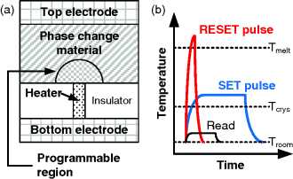
Figure 5.1 (a) Cross-section schematic of a conventional phase change memory cell. The electrical current passes through the phase change material between the top electrode and heater. Current crowding at the “heater” to phase change material contact results in a programmed region illustrated by the mushroom boundary. This is typically referred to as the mushroom cell. (b) PCM cells are programmed and read by applying electrical pulses to change the temperature inside the PCM cell accordingly. © IEEE. Reprinted with permission, from [7]
PCM uses the large resistivity contrast between the crystalline (low resistivity) and amorphous (high resistivity) state of a phase change material in order to store the information. This phase (resistivity) change is achieved by applying sufficient thermal energy to change the phase of the material. In order to reset the PCM cell into its amorphous state, a short electrical pulse (typically<50 ns) is applied to the bottom electrode contact (BEC). The amplitude of the pulse is such that the heat generated in the phase change material–heater interface causes a region of the phase change material to melt. The thermal pulse is quenched rapidly to cause the molten region to cool to its amorphous state. For the case of set programming, the PCM cell is applied an electrical pulse that is sufficient to increase the temperature of the programming region above the crystallization temperature and a time period sufficiently long to crystallize the phase change material. To read the state of the cell a small electric pulse is applied to measure the cell resistance such that it does not disturb the state of the cell. The different pulse shapes are summarized in Figure 5.1b.
The current–voltage characteristics of the set and reset states are shown in Figure 5.2. It can be seen that there is a large resistance contrast between the set and the reset state for voltages below the threshold switching voltage (Vth). The cell in the reset state has a high resistance below Vth and shows electronic threshold switching behavior at Vth, that is, a negative differential resistance. For voltages below Vth (sub-threshold region) the PCM returns to its original amorphous state after removing the electrical stimulus. However for voltages above Vth, when the electrical stimulus is retained for a sufficient amount of time, the PC material undergoes memory switching into a low-resistivity, crystalline state. The programming of the PCM cell critically depends on this electronic threshold switching process [6], the physics of which is yet to be fully understood. The conduction of high current through the amorphous region is enabled only by this switching process in order for the crystallization process to occur.
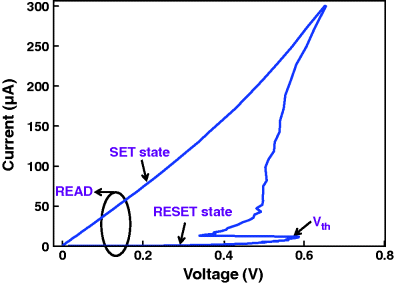
Figure 5.2 I–V characteristics of the SET and RESET states. The RESET state shows switching behavior at the threshold switching voltage (Vth). The RESET state stays in the high resistance state below Vth (sub-threshold region) and switches to the low resistance state at Vth
Reset programming consumes the largest power since the cell needs to reach the melting temperature of about 600 °C. The reset current required for the cell to reach this melting temperature depends on a number of factors such as the electrical resistivity and thermal conductivity of the materials used as well as the specific device structure (which determines the thermal environment of the device). The set programming however limits the operating speed of the PCM as it takes longer time to crystallize the amorphous region.
5.3 Material Properties
The active material of a PCM cell is the phase change material that determines the majority of the device characteristics. These materials have three major requirements: bistability of the amorphous and crystalline states, ability to rapidly switch between the two states, and high electrical resistance or optical reflectivity contrast between the two states. While most known phase change materials can exist in both a glassy and crystalline state, few have both the biphasic stability and suitable transition dynamics between both phases required for memory applications. More specifically, crystallization time of materials varies significantly, but only values in the nanosecond regime are viable candidates for commercial applications. These requirements significantly limit the range of viable materials for PCM to those mostly in the chalcogenide family (Group 16 elements, primarily S, Se, and Te). Despite the discovery of the switching phenomenon in the 1960s [1] the technological success of optical storage based on phase change materials was only possible after the discovery of a new class of materials that fulfilled the requirements of this technology. The chalcogenide alloys along the GeTe-Sb2Te3 pseudo-binary line (Figure 5.3) are among the most commonly used materials because of their large optical and electrical contrast and faster crystallization times. The discovery of this class of chalcogenide alloys led to a very successful re-writable storage technology with its third generation 100 GB capacity Blu-ray disks [9]. In addition, the excellent electrical and scaling properties of these materials sparked a new interest in early 2000 for these materials to be used in nonvolatile memory applications [2]. The following sections describe in detail the different aspects of the phase change material properties that make PCM a potential candidate for the future nonvolatile memory technology.
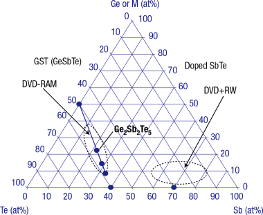
Figure 5.3 The most popular phase change material GST 225 falls in the tie-line between GeTe and Sb2Te3. © Nature. Reprinted with permission, from [8]
5.3.1 Electrical and Phase Transformation Properties
The electrical resistivity contrast between the crystalline and amorphous (as-deposited) state in phase change materials can be up to five orders of magnitude [10]. Figure 5.4 shows the resistivity change with temperature for different class of phase change materials. It can be seen that there is a sudden drop in the resistivity at a particular temperature and this temperature is commonly referred to as crystallization temperature (Tcrys). Materials need to be chosen such that the Tcrys is high enough to ensure proper retention of the amorphous state for 10 years at the operating temperature of the PCM cells, that is, 85 °C for embedded memory applications and 150 °C for automotive applications. In contrast to the above requirement, the materials must undergo phase transformation in the nano-second regime to meet the memory application requirements. These are very conflicting requirements and a number of different alloy compositions and doping techniques [11] have been studied to identify the desired material composition that meets the specifications of both the retention and speed for nonvolatile memory applications. Recently, a N-doped GST alloy [12] achieved retention at 120 °C for 10 years that meets the requirements for industrial and some automotive applications.
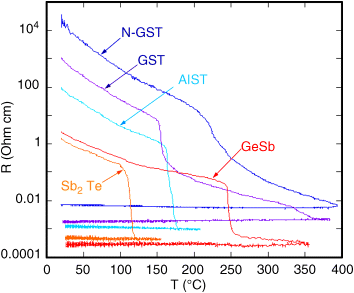
Figure 5.4 Resistivity as a function of temperature during a heating cycle at 1 K s−1 for initially amorphous, as-deposited 50 nm films of various phase change materials. Initially, the thin films have a high resistance that drops sharply when the crystallization temperature is reached, and it stays low upon cooling. GST – Ge2Sb2Te5, N-GST – 7 at% N doped GST, GeSb – Ge:Sb ratio 15:85, AIST – Sb2Te doped with 7 at% Ag and 11 at% In. © Journal of Applied Physics. Reprinted with permission, from [10]
5.3.1.1 Conduction Mechanism and Threshold Switching
The electrical conductivity in the amorphous phase can be described by thermally activated hopping transport [13] as shown in Figure 5.5. A Poole–Frenkel (PF) transport of carriers through traps leads to a current which is linear with voltage for very small voltages and exponential for high voltages. The trap energies are randomly distributed in the band gap of the amorphous material and the PF conduction happens through preferred filamentary paths that have the least overall activation energy [14]. At a certain material-dependent threshold field on the order of 10–100 V μm−1 [15] the resistivity of the amorphous phase change material suddenly decreases by orders of magnitude, negative differential resistance is observed, and so-called threshold switching occurs (Figure 5.2). The mechanism behind threshold switching is still not fully understood and several models have been proposed as a possible mechanism. The Joule Heating model [16] attributes the threshold switching to thermal runaway within the chalcogenide layer. This model is based on a simple observation that the current through the phase change material increases exponentially due to the temperature-dependent conductivity of the phase change material as temperature increases. However, since the speed of switching is faster than the thermal time constant, electronic mechanisms are favored over purely thermal mechanisms [17]. In the Impact Ionization model, for higher electric fields the current rises exponentially due to secondary carrier generation in the amorphous region. The electrons get trapped in the donor-like traps. But as the field increases, all the trap states are filled and the free carrier density increases. The impact ionization overcomes the carrier recombination process, the traps are filled and the voltage snap back occurs. As a result, higher current can flow through the device at a lower voltage and the impact ionization process still happens but with a lower multiplication rate [18–20]. In another electronic model, threshold switching is attributed to energy gain of electrons in a high electric field leading to a voltage–current instability [6]. In the field-induced nucleation model [21], threshold switching is explained based on the electric field assisted formation of crystalline nuclei across the programming region. These crystalline nuclei disappear if the electric field is removed prematurely and would go back to its original amorphous form. There is no experimental demonstration as to which of the above models correctly explains the physics behind the threshold switching. The dominant switching mechanism may depend on the material system and more than one mechanism might be required to explain the experimental observations at different operating conditions or device dimensions. The electrical conduction in the crystalline phase of the phase change material can be described straightforwardly with the drift diffusion behavior of a doped semiconductor resulting in Ohmic behavior at low voltages [18]. NonOhmic behavior of PCM cells for higher voltages can be attributed to Joule heating by the current causing the temperature-dependent resistance to change.
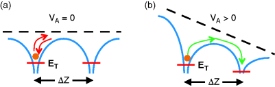
Figure 5.5 (a) Schematic showing the carrier trapped in the localized states of the amorphous phase change region at the trap energy ET. The inter-trap spacing is Δz (b) On applying a bias voltage VA across the amorphous region the barrier height to the carrier hopping is reduced enabling them to hop from one trap to the other easily, resulting in sub-threshold conduction [139]
5.3.1.2 Resistance Drift
The phase transformation to the amorphous state is achieved either by ion implantation [22] or by melt-quenching with an electrical/optical pulse. The amorphous state resistance of a PCM cell, measured at a given read voltage is determined by the nature and volume of the amorphous region formed during the reset programming. The amorphous resistance does not remain constant but rather drifts logarithmically with time to a higher value immediately after the reset pulse is removed following the power law R = R0 × (t/t0)ν where R and R0 are the present and initial resistances, t and t0 the present and initial times, and ν the drift exponent [23]. This phenomenon is called resistance drift. Figure 5.6 shows the change in the amorphous resistance of a PCM cell over time for different reading temperatures immediately after reset programming [24]. The drift is also a strong function of the temperature [25] and the volume of the amorphous region [26]. Higher temperatures and larger amorphous volumes have larger drift coefficient. The threshold voltage also shows a similar behavior with time [27]. While resistance drift to higher values increases the on/off ratio for two-level memory, it is a major problem for the multi-level PCM implementation [28] because the different resistance levels overlap as time progresses and is no more distinguishable from each other. There is currently no consensus on what causes drift, but there are two major theories that explain as to why drift occurs in PCM. According to the Structural Relaxation (SR) model, drift is explained as a reduction in the number of structural defects (distorted bonds, wrong bonds, vacancies, etc.) that causes an increase in the band gap and of the activation energy for conduction [23,24]. In other words, the density of traps decreases with time due to reduction of the structural defects, causing the trap spacing to increase, which in turn raises the barrier for PF conduction through the trap states. Alternatively, resistance drift is explained as the relaxation of the compressive stress developed in the amorphous phase at solidification [29]. In fact, the density of the amorphous phase is 6.5% lower than the crystalline phase, thus possibly causing a compressive stress after reset programming in PCM cells where the amorphous region is surrounded by a crystalline region. Experimental results on nanowire PCM devices indicate that the drift coefficient decreases with the size of the phase change nanowire [29]. The results also show that the drift exponent is higher for nanowires encapsulated with nitride or oxide, presumably due to the enhancement of the local stress by mechanical confinement. However, a recent study on PCM thin films and devices subjected to external mechanical stress [30] suggests that the resistance drift is primarily due to structural relaxation and not by any mechanical stress relaxation. There is still a lack of proper systematic study explaining the direct impact of mechanical stress on PCM devices and whether there is any correlation between the two theories.
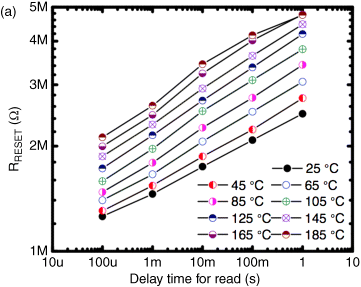
Figure 5.6 Reset resistance as a function of time after reset programming for various annealing temperatures (TA). Cells are programmed and read at room temperature, 25 °C [27]. © IEEE. Reprinted with permission, from [140]
5.3.1.3 Mechanism of Crystallization
When the electric pulse is applied for a sufficient amount of time after the threshold-switching event, the amorphous region is transformed into its crystalline phase provided the temperature reaches above the crystallization temperature, but below the melting temperature; this process is called crystallization. The nucleation and growth processes govern the crystallization kinetics of PC materials. Nucleation involves the formation of small crystalline nuclei in the amorphous matrix, and growth involves the subsequent expansion of the phase front separating the amorphous and crystalline regions. The driving force for crystallization is the gain in free energy below the melting temperature. While similar in bonding structure, common phase change materials are traditionally divided into two categories based on their crystallization kinetics: growth-dominated materials and nucleation-dominated materials [31]. (Figure 5.7) Growth dominated materials are generally related to the family of AgIn doped Sb2Te (AIST) materials, and are characterized by slow nucleation, but fast growth of crystalline domains. In contrast, the prototypical nucleation dominated material is Ge2Sb2Te5 (GST) where nucleation events happen quickly during crystallization. Nucleation-dominated materials generally fall on the tie-line between GeTe and Sb2Te3 whereas growth-dominated materials contain much more antimony. (Figure 5.3) In case of the growth dominated materials, the time it takes for crystallization (tcrys) depends on the size of the amorphous region, while it is independent in case of nucleation dominated materials [31]. It has been shown that, in the case of highly scaled PCM devices, the growth dominated phase change materials enable faster crystallization times because of the smaller amorphous volume [33]. The dynamics of crystallization (phase change) in GST and related systems have been fairly well interpreted in terms of the classical nucleation and growth model developed by Kolmogorov, Johnson and Mehl, and Avrami (KJMA model) [32]. The KJMA model gives the macroscopic evolution of the transformed phase under isothermal annealing condition and has been extended to analyzing transformations under a constant heating rate. Recently [34], a modification involving the introduction of fractal geometry and the Meyer–Neldel rule [132] for thermally activated processes was introduced into the KJMA theory to account for the deviations in the measured physical parameters like Avrami exponent (n) and frequency factor (ν). Further a number of other crystallization models [35,36] have been proposed that considers the effect of percolation effects and local temperature effects in practical PCM devices. For the same target resistance, the type of the programming scheme used can also result in different crystallization times due to the variations in the nature of the amorphous volume formed during the programming [37]. Furthermore, fast crystallization times can be correlated to the structural properties of the phase change materials. Fast switching materials often show a simple cubic or rocksalt structure with random atomic distributions that require little atomic movement to change from the amorphous to the crystalline state [38]. In addition it was found that resonance bonding [39] plays an important role for fast switching of phase change materials [40]. A low degree of ionicity and low tendency towards hybridization is typical of fast switching phase change materials [41]. Recently, it was shown that a small incubation electric field could be used to produce rapid crystallization within a few hundred ps, up to an order of magnitude faster than the conventional crystallization times of >10 ns [42]. This electrical controllability of the crystallization speed is attributed to the temperature rise due to the small incubation field which is sufficient to cause a prestructural ordering of the local cluster of atoms, but still small to start the crystallization process. Recent studies [43] also show that decreasing the grain size of the deposited phase change material can significantly reduce the crystallization time of the cell because of the presence of a large number of broken or loosely bonded atomic structures at the grain boundaries. The process of crystallization has also been studied in different phase change materials [44,45] using density functional simulations to understand different bonding reconfigurations that happens at the atomic level. Hence, understanding the crystallization process and related parameters can guide us to explore novel materials with improved retention and switching characteristics.
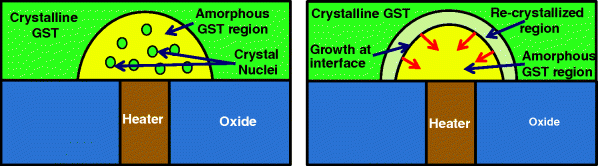
Figure 5.7 Nucleation and growth dominated phase change materials
5.3.1.4 Mechanism of Amorphization
The process of amorphization is traditionally considered to involve melting the phase change material and rapidly quenching it to the room temperature. This results in the formation of a large number of dislocations or vacancies in the programmed region and thereby resulting in high resistance. However, some of the recent studies [46–48] show that it is possible to bring about crystalline to amorphous phase transformation without actually going through the molten state. Ultra-fast photo excitation methods were employed to provide sufficient energy to trigger the rupture of the sacrificial (resonant) bonds that are inherently present in the crystalline phase of the GST to collapse to its amorphous phase without actually melting the material [47]. This photo-induced lattice instability requires about five times less power than that of the conventional melting process. Studies using nanowire PCMs [48] show that amorphization can also occur as electrical fields drive the movement of dislocations in the crystalline phase to move in the direction of the E-field to be collected as a narrow amorphous region resulting in a sudden increase in the device resistance. Further, the recent demonstration of low-power amorphous switching in superlattice-based interfacial PCM [40] and small grain PCM devices [43] can be explained based on the fact that these devices have a large number of interfaces/grain boundaries in their programmed volume where the resonant bonds/dislocations play a major role in the phase transformation. The above studies are only the first step in understanding the physics behind the phase transformation of these unique nanoscale class of materials and further research in this area can help us engineer highly energy efficient and ultra-fast phase change memory devices.
5.3.2 Thermal and Mechanical Properties
The programming of PCM is achieved by Joule heating of the phase change layer to temperatures above the melting temperature. The current required to achieve this temperature depends strongly on the thermal properties of the various materials that form the PCM device namely the phase change layer, heater electrode, top electrode and the surrounding dielectrics. The thermal resistance arising from carrier energy scattering in the bulk of the material and the thermal boundary resistance (TBR) arising from scattering in the interface region are the two main mechanisms that contribute to the overall thermal network of the PCM cell [49]. Hence, understanding thermal conduction in thin film phase change materials, thin film electrode materials, and at their interfaces is essential for reducing the programming energy.
The most common thin film thermal conductivity measurement techniques for phase change materials are the 3ω method [50], nanosecond transient thermoreflectance (TTR) [51], and picosecond time domain thermoreflectance [52,53]. Measurements on the common phase change material GST show thermal conductivities at room temperature in ranges of 0.14–0.29, 0.28–0.55, and 0.83–1.76 W m−1 K−1 in the amorphous, rocksalt, and hexagonal phases, respectively [54]. The rocksalt phase thermal conductivity exhibits a slow increase with temperature consistent with other highly defective crystalline materials [52,53]. Recently, high density nanostructured materials have exhibited thermal conductivities as low as 0.05 W m−1 K−1 [55]. Nanostructured phase change regions [40,43] have the potential to offer dramatically reduced programming currents through exceptionally low thermal conductivities. Another key challenge is extending thermal conductivity measurements to the melting temperature, which is notoriously difficult due to the volatility of many phase change materials at high temperatures. These measurements will shed light on the relative electron and phonon contributions in conduction at device operating conditions, informing better material selection. There have been many studies [51,53] of the thermal conductivity normal to GST films (knormal), but the in-plane thermal conductivity (klateral) or the conductivity anisotropy can also be an important factor that determines the programming current. Thermal conductivity anisotropy in thin films can be due to electron or phonon scattering on film interfaces, partially oriented grains or inhomogeneous material quality [56]. Lateral thermal conduction in GST films can also negatively affect the thermal cross talk in high density cells and the programming current of PCM devices, the latter being more pronounced for novel lateral designs. The anisotropy ratio (klateral/knormal) depends on the annealing time and temperature of the deposited phase change films [57] and can reduce the programming current by up to 40% [56].
Much of the heat generated during GST cell switching occurs in the GST bulk and at the bottom electrode interface [58,59]. Coupled electrical–thermal simulations revealed that the programming current of a PCM device decreases by as much as 30% for GST-electrode TBR values of 50 m2 K GW−1 [59]. In many PCM designs, significant heat loss occurs through the electrode [60–62] due to the large thermal conductivity of the heater material such as TiN ∼8 W mK−1 compared to the GST ∼0.4 WmK−1 (Figure 5.8). This problem can be alleviated by introducing alternative electrode materials such as C and W-WNx [62] or by inserting low thermal conductivity TaN electrodes within a TiN electrode [63]. Engineering the electrode to have acceptable electrical conductivity and very low thermal conductivity is a key step toward reducing programming current. Composite electrodes may leverage TBR to increase the device effective thermal resistance.
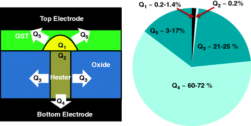
Figure 5.8 Percentage of energy dissipated in different regions of PCM [60]. The useful energy spent in bringing the phase transformation (Q1, Q2) is much smaller compared to the rest of the energy that is dissipated through the surroundings
The large current density and temperature excursion exceeding 600 °C in the phase change layer gives rise to a more pronounced effect of the thermoelectric properties such as the Seebeck effect on the programming properties of a PCM cell. Recent measurements provided evidence of thermoelectric transport in PCM cells through observation of a modification in the amorphous region [64] and the programming condition [65] with the bias polarity. The Seebeck coefficient of Ge2Sb2Te5 films shows strong dependence on temperature and temperature history as governed by the phase purity. It scales with film thickness due to varying degrees of crystallization and phase purity in crystalline GST films [66]. Recent electrothermal simulations indicated nearly a 45% increase and 16% decrease in the peak temperature and programming current, respectively, if thermo-electric effects are considered [67].
From this discussion it is clear that the search for the best phase change material is a multi-parameter optimization process with some seemingly contradictory requirements such as high stability of the amorphous phase at operating temperature, but very fast crystallization of the amorphous phase at switching temperature. Many material parameters will also change with size of the phase change material when devices are scaled to nanoscale dimensions. Much research is still required to understand the fundamental relationship between material composition and structure, and phase change properties for a physics/chemistry-based design of new phase change materials.
5.4 Device and Material Scaling to the Nanometer Size
One of the major advantages of PCM over the conventional FLASH technologies is its scalability to sub-10 nm dimensions. However it is unclear how properties would change both at the material and at the device level. This section summarizes some of the recent works on how the material physics and the device properties change as we enter technology nodes on the order of the grain size or the trap dimensions of phase change materials.
5.4.1 Materials Scaling Properties
Nanomaterials have properties that are different from bulk materials of the same composition because surface and interface atoms play an increasingly important role in determining the different material properties. It is important to know how phase change material properties change with size in order to be able to evaluate the scalability of PCM technology. It is predicted that as the volume of phase change material gets smaller, the phase stability characteristics will change. Since PCM relies on the bi-stability of the amorphous and crystalline phases, the technology will only be reliable as long as both states are distinct. It is conceivable that there is a limit to the minimum number of atoms required for the two phases to be distinct, and that there is a minimum size at which both phases are stable under the conditions required for commercial applications.
Scaling studies of phase change materials have been done on thin films, nanowires, nanoparticles, and PCM devices (see [68–70] for overviews). It was found that many properties of the phase change materials do depend on size, in particular below the 10 nm range. These changing properties include crystallization temperatures and times, related activation energies for crystallization, melting temperatures, resistances, and optical and thermal properties. Crystallization temperatures can vary up to 200 °C and can be increased or decreased for very thin phase change films depending on the interface material [71,73] which in turn also significantly affects the crystallization time of the material [73]. Melting temperatures are reduced for thinner films [69], hence potentially reducing the power to melt-quench the material. Electrical resistances on the other hand are increased as film thickness is reduced [72].
While these dependencies increase the complexity of materials optimization they also enable us to tune interfacial properties in such a way that desirable switching properties are obtained. Nanostructured materials such as the multi-layered superlattice-like (SLL) structures have switching properties that are significantly different from the bulk materials [74]. In PCM, higher heterogeneous crystallization rates can be achieved in the nanostructured phase change materials due to their high surface area to volume ratios [75]. Nanoscale active device regions or volume of phase change materials can also have lower phase-transition temperatures than the bulk materials due to greater phonon softening effects [76,77]. Materials with SLL structures have lower thermal conductivities than the bulk materials with the same composition [78]. They also have favorable thermal confinement properties due to the phonon scattering effects at the interfaces [79]. Phase change materials with SLL structures can be formed by alternating layers of Sb2Te3 and GeTe, which have fast switching speed and good data retention, respectively [78,80].
Recently, a superlattice-like structure of GeTe/Sb2Te3 of thicknesses between 5 Å and 40 Å was used to fabricate a PCM cell called Interfacial PCM (IPCM) [40], (Figure 5.9) that shows excellent endurance properties and requires an order of magnitude lower switching energy than the conventional single layer GST cells. These excellent switching and endurance properties of IPCM is due to confinement of the atomic movements to a single dimension, that is, the interface between GeTe and Sb2Te3 controls the local atomic switching of Ge atoms resulting in a phase transition with substantially reduced entropic losses. The ultrathin, uniform stratum of Sb2Te3 and GeTe lowers the entropy of the covalent amorphous state by restricting the number of atomic configurations that can exist. For the SET operation, IPCM-based devices use only 12% of the energy required by similar GST-based devices. This increase in efficiency means less energy is dissipated during the phase transition, which in turn leads to more than an order of magnitude improvement in the SET–RESET cyclability. Reducing the entropic losses has further ramification of producing highly repeatable device characteristics. Indeed, the resistance of the IPCM during the SET–RESET cycle is identical over a million cycles.
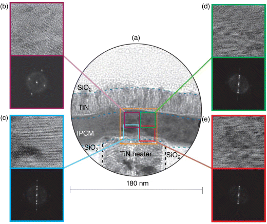
Figure 5.9 TEM image of a (GeTe)2(Sb2Te3)4 Interfacial Phase Change Memory (IPCM) in the RESET state. The diffraction data (b–e) at different locations above the electrode shows that (b) the layered structure of the IPCM is preserved even after RESET, implying that the layers did not undergo any melting during the programming operation. © Nature. Reprinted with permission, from [40]
Engineering the grain-size of the as-deposited phase change material can also result in improvements in switching speed and reduced switching energy. GST with small grain sizes have high interface area to volume ratios, which can promote hetero-crystallization (interfacial growth) at the grain interfaces or boundaries [81]. These can alter the phase change mechanism of GST from a nucleation-dominated mechanism to a growth-dominated mechanism, enabling faster crystallization. The increased number of grain boundaries also decreases the thermal conductivity of GST [56]. This increases the thermal confinement in cells, thus reducing the power needed for RESET. The large surface to volume ratio in these materials also facilitates stress relaxation after RESET and hence results in a lower resistance drift compared to the bulk GST. Overall, the scaling properties of nanostructured phase change materials are promising for the development of the fastest and the most efficient phase change memory devices that will be required to meet the demands of the future technology.
Phase change nanoparticles offer another intriguing way of understanding the scaling properties of many chalcogenide materials. A number of techniques have been used to synthesize nanoparticles, including pulsed laser ablation [82,83], electron-beam lithography [10], selfassembly-based lithography techniques using sputter deposition [84,85] or spin-on phase change materials [86], and solution-based chemistry [87]. Large nanoparticles show properties similar to bulk, but the small nanoparticles below 10 nm show size-dependent properties such as higher crystallization temperature and reduced melting temperature. Both are beneficial for PCM applications and illustrate the favorable scaling properties of phase change materials. GeTe nanoparticles can be synthesized in the amorphous phase and can be crystallized by heating them over their crystallization temperature (remarkably increased compared to bulk) for nanoparticle sizes as small as 1.8 nm [87]. As such, GeTe nanoparticle is a convenient material for exploring the ultimate size limit of PCM. Figure 5.10 shows transmission electron microscope images of these GeTe nanoparticles of various sizes. Down to these small sizes, phase change materials still show phase transformation. These nanoparticles are as small as about two to three times the lattice constant, so this will be close to the ultimate scaling limit of phase change technology as far as the phase change materials themselves are concerned.
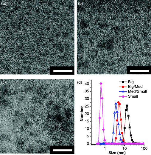
Figure 5.10 TEM images of size-selected samples of amorphous GeTe nanoparticles. All scale bars are 10 nm. (a) Small nanoparticles of 1.8 ± 0.44 nm. (b) Medium nanoparticles of 2.6 ± 0.39 nm. (c) Large nanoparticles of 3.4 ± 0.74 nm. (d) Dynamic Light Scattering results of another instance of size-selected nanoparticles. See http://pubs.rsc.org/en/content/requestpermission?msid=b917024c. © Journal of Materials Chemistry. Reprinted with permission, from [87]
The future challenges for the material scientists from the technological standpoint will include exploring phase change materials that do not exhibit void formation or elemental segregation, tailoring the increasingly important interfaces that support high cyclability, good data retention, and fast switching, and continuing the study of scaling properties of phase change materials as dimensions shrink to the few-nanometer length scale.
5.4.2 Device Scaling Properties
While it has been established that phase change materials (e.g., GeTe) can exist in two stable phases, it is still necessary to explore how the memory device characteristics may behave when PCM are scaled to nanometer size. The active device area of the phase change memory needs to be scaled every year in order to meet the demands of the increasing device density. Furthermore, device scaling has the advantage of reduced programming power. Table 5.1 summarizes the scaling rules for both isotropic and aggressive scaling. There are two major device properties that are significantly affected by the scaling of the active device, namely the threshold switching voltage and the reset current. Several device structures and methodologies have been used to understand how scaling affects these device parameters and will be discussed below.
Table 5.1 Scaling rules of PCM cell for both isotropic and aggressive scaling. k ∼ 1/F with F being the feature size
| Parameters | Scaling factor | |
| Isotropic | Aggressive | |
| Heater contact area | 1/k2 | 1/k2 |
| Vertical dimensions | 1/k | 1 |
| Electrical/thermal resistances | k | k2 |
| Power dissipation | 1/k | 1/k2 |
| Current | 1/k | 1/k2 |
| Voltage | 1 | 1 |
| Current density | k | 1 |
5.4.2.1 Threshold Voltage Scaling
The present models for threshold switching are based on the inter-trap distance [13] or the minimum distance that the carriers have to travel to cause impact ionization [18]. It is not clear how threshold switching properties will change when the film thickness becomes comparable to either of these distances. A number of device structures ranging from phase change bridge cells to electrodes of carbon nanotubes have been used to study how the threshold voltage scales as the size of the active programming region decreases. In [88], an additional top electrode was introduced in the GST layer at a specific height from the bottom electrode of the PCM cell to confine the programming volume to a specified thickness. It has been shown that the threshold switching voltage linearly increases with GST layer thickness with a nonzero offset. In the case of nanowire PCM devices [75,89] the threshold switching voltage scaling changed from constant field to constant voltage scaling with the length of the amorphous region below 10 nm. The phase change bridge (PCB) device is another cell design uniquely suited to study the electrical scaling characteristics of phase change materials [90]. It comprises a narrow line of thin phase change material bridging two underlying electrodes. The PCB structure is ideally suited for a variety of characterization experiments [15,91]. For instance, in Figure 5.11 the critical field necessary for threshold switching for different materials has been obtained by plotting the measured threshold voltage of the PCB device as a function of the device length. The threshold fields for Ge15Sb85, Ag- and In-doped Sb2Te, Ge2Sb2Te5 and 4 nm thick Sb devices are 8.1, 19, 56, and 94 V μm−1, respectively. Recently, carbon nanotubes (CNTs) with diameters of ∼1 to 6 nm were used as electrodes to reversibly induce phase change in nanoscale GST bits [92]. The study also demonstrates reversible switching with programming currents from 0.5 to 8 μA, two orders of magnitude lower than state of the art PCM devices. The active device area is the small nanoscale gap formed in the middle of the CNTs through electrical breakdown [133]. By controlling the breakdown voltage, gaps ranging from 20 to 300 nm was formed. Threshold voltages scale proportionally to the size of the nanogap, at an average field of ∼100 V μm−1 for GST material.
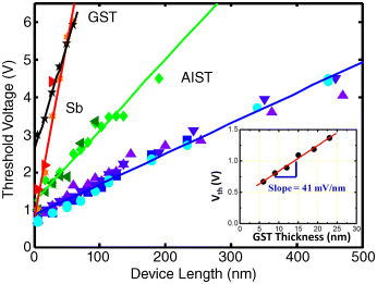
Figure 5.11 Scaling of threshold voltage with the length of the active phase change region in a phase change bridge device (Device Length). Results are shown for four different phase change materials. The slopes of the linear fits are used to determine the threshold fields for each material. © Journal of Applied Physics. Reprinted with permission, from [15]. Interestingly all these materials have nonzero threshold voltages. Inset shows similar threshold voltage scaling on vertical PCM devices using GST. The linear threshold voltage scaling applies to thicknesses as small as 6 nm. © IEEE. Reprinted with permission, from [88]
5.4.2.2 Reset Current Scaling
The large programming current is still a key issue that limits the adoption of PCM in many applications. Furthermore, a large programming current in PCM imposes a stringent requirement on the current delivered by the memory cell selector integrated in series with the PCM. In order to provide the current required to switch the states of PCM, the area of the memory cell selector may not be scaled down as fast as the memory cell itself, thus the size of the cell selection device becomes the limiting factor for device density and annihilates the small size advantage of PCM technology. Therefore, reducing the programming current is necessary for achieving both high density and low power consumption of PCM.
To decrease the reset current, one way is to increase the heater thermal resistance by reducing the contact area [4]. The feature size of the conventional mushroom structure (Figure 5.1) of PCM is limited by lithography and process capability. This was recognized early on and many innovative device structures have been explored to reduce the effective bottom electrode contact (BEC)/GST interface to the sub-lithographic regime. Figure 5.12 shows the reset current reduction as a function of the equivalent diameter of a circular contact and the effective contact area for different cell structures, such as conventional mushroom type [93], edge contact type [94], μTrench [95], cross-spacer PCM [96], “wall” structure [97], “pore” structure [98], ring type contact [99], and dash-type confined cell [100]. We can clearly see that the reset current scales with the effective contact area of the PCM and that a constant current density ∼40 MA cm−2 is required to program an average PCM cell. Those with carefully engineered cell structures and materials can be programmed using ∼10 MA cm−2. Recent demonstrations of PCM devices using CNT as the electrodes [92,101] show extreme scalability of the reset current down to 1 μA range. These PCM devices have an active area of only a few nm2 because CNT diameters are only about 1–2 nm. They demonstrate typical electrical switching characteristics that are observed in larger devices. This shows that, the scalability of the phase change material properties can also be observed in practical device configurations [101] and hence providing for a viable technology that can extend the semiconductor memory device scaling for several generations.
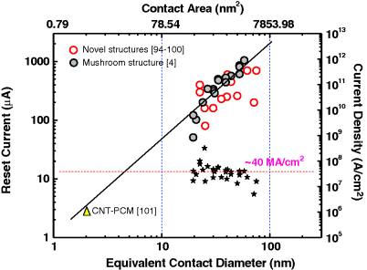
Figure 5.12 Reset current as a function of equivalent contact diameter, showing a linear scaling trend with the effective contact area as the device feature size goes down. A constant ∼40 MA cm−2 current density is required to program the PCM cell. © IEEE. Reprinted with permission, from [7]
5.5 Multi-Bit Operation and 3D Integration
The advancements of the phase change memory cell itself does not guarantee the success of this technology for practical applications. In order for PCM to be commercialized in a large scale we have to increase the available storage capacity per unit area of memory. Multi-level operation and multi-layer 3D stacking are two possible ways of achieving this goal. In this section we will see some of the major advances and the challenges that we face in this field and also discuss the issues that we need to consider as we scale to large array sizes.
5.5.1 Multiple Bits per Element
Multilevel cell (MLC) storage is essential for reducing the cost per bit of PCM technology and for increasing its potential for market acceptance. The large resistivity contrast between the crystalline and the amorphous state of the phase change materials and the ability to access the intermediate states in a reliable way have made possible the realization of multi-level implementation in PCM. Some of the earlier methods of MLC implementation are based on engineering the properties of the chalcogenide layer by doping [102,103] or by stacking multiple layers with differing electro-thermal properties as the storage medium [104–106] or by using parallel combination of multiple resistances [107,108]. These demonstrations thus depended on precisely engineering the cell structure to achieve the intermediate resistance states. However, even conventional cell structures such as the common “mushroom” phase change element could be programmed to store multi-bit data by altering the size of the amorphous region in a continuous manner to achieve different resistance levels. The size changes as a function of the amplitude of the write pulse, as quantified by the cell's programming curve shown in Figure 5.13a. However, process and material variations give rise to resistance levels with broad distributions when single programming pulses are applied. A common solution is to employ iterative programming schemes, in which a sequence of write and verify steps is used in a feedback loop to minimize the error between the programmed and a specified target resistance level. A basic iterative scheme is shown in Figure 5.13b. It was shown that by varying the amplitude or slope of the trailing edge of the programming pulses to control the evolution of temperature in the cell, up to 16 intermediate levels could be programmed in a cell, thus demonstrating a four-bit cell [109]. These programming techniques are based on the fact that the cell resistance Rcell can be increased by applying programming pulses of larger amplitudes that result in melting of larger volumes of the amorphous region (partial RESET), or can be decreased by applying pulses of lower amplitude (partial SET), or sequences of annealing pulses of appropriate magnitude to crystallize and shrink the size of the amorphous volume [110]. A novel iterative programming scheme that uses both partial-SET and partial-RESET pulses is depicted in [111]. Operation starts from the partial-SET regime and either terminates there if the target resistance is reached, or switches to the partial-RESET regime if the programmed resistance drops below the target level. This hybrid method combines the low energy dissipation of the partial-SET regime with the flexibility of achieving higher or lower resistance level using the partial-RESET regime.
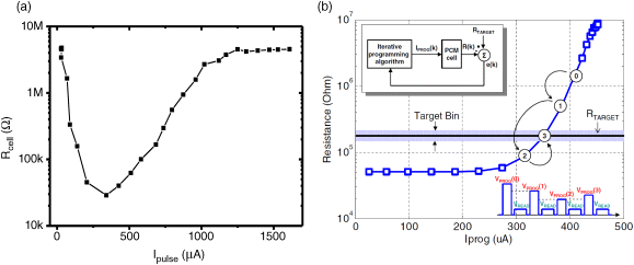
Figure 5.13 (a) Typical Rcell–Ipulse curve obtained by varying the current pulse amplitude for a mushroom phase change memory cell. © IEEE. Reprinted with permission, from [103]. (b) Schematic illustrating the basic iterative programming concept using a sequence of adaptive write and verify steps. © IEEE. Reprinted with permission, from [112]
Regardless of how much efficient the MLC scheme can be in producing tight and dense resistance distributions, the resistance drift adversely affects the reliability of MLC storage in PCM, because the distance between adjacent levels is small and stochastic fluctuations of the resistance are more likely to cause level overlap over time than in binary storage. Currently there is no known material solution to mitigate the effect of drift, as the physics of drift in itself is not well understood. However, a novel drift-resilient MLC PCM state metric has been proposed for MLC programming that is largely robust to the impact of drift [112]. Traditionally, the low field resistance is used as a metric to define the different MLC levels. This resistance value is a strong function of the activation energy (Ea) and suffers a large change as Ea changes with time during the drift phenomenon [28]. Instead, what is required for drift-tolerant MLC is a cell state metric that has minimal dependence on the activation energy, but has a linear relationship to the amorphous thickness. To achieve this, the read voltage is progressively increased until a certain predefined current level IR, is reached. This current level is chosen to be a safe value much below the current needed for threshold switching to occur. The time needed to reach IR can be considered as a measure, M of the programmed state. It is shown that M is proportional to the effective amorphous thickness [112], yet it is a weak function of the activation energy (nearly linear as opposed to exponential), suggestive of a significant tolerance to drift. Experimental results suggest that the new metric has an order of magnitude smaller drift coefficient than the standard resistance metric. In another approach, the effect of drift on the selected cells was predicted by using reference cells that have similar thermal history and undergo same drift behavior [113]. Another way of mitigating the impact of drift on the resistance levels is by using an additional annealing pulse to accelerate the drift immediately after the reset programming [114,138]. This additional pulse quickly anneals out many defects (that are responsible for the drift) and provide a drift-free period that enlarges the read window. This technique not only reduces the read latency but also enables a more reliable read window for multi-level applications.
5.5.2 3D Stackable Memory
A vision for high density memory is the cross-point architecture with a memory cell integrated with a cell selector within a 4F2 footprint that can be stacked in the third dimension Figure 5.14. To realize this, the selector should have a 4F2 footprint that can be scaled with the bitline/wordline pitch [134,135], a small off current, and an on-state current that is sufficient for programming the memory (the reset current for the case of PCM). Furthermore, the fabrication process should be compatible (e.g., material and process temperature) with CMOS BEOL and the memory cell. The trend for the reset current in Figure 5.12 shows an average of 40 MA/cm2 with the lower bound of about 10 MA/cm2. This large current is fairly difficult to achieve even for single crystal silicon diodes. A number of recent efforts have been made to integrate a memory cell selector with a phase change memory cell. Sasago et al. [93], used a low-thermal budget process to fabricate a 4F2 poly-Si diode with a drive current capability in excess of 8 MA cm−2 and on-off ratio more than 104. Kau et al. [115] used a stackable cross-point phase change memory utilizing the Ovonic threshold switching (OTS) property of chalcogenide materials to make the memory cell selector. Since both the memory device and the selector exhibit threshold switching behavior, the programming voltage conditions have to be carefully chosen to avoid disturbing the state of the cells in the un-selected bit and word lines. Gopalakrishana et al. [116], proposed an access device based on Cu ion motion in novel Cu containing Mixed Ionic Electronic Conduction (MIEC) materials. These MIEC-based devices can be fabricated at <400 °C, are scalable, and can conduct very high current densities (up to 50 MA/cm2) – making them suitable for stacking of multilayer PCM arrays in the BEOL. Sasago et al. [117] proposed another stackable access device structure in which the phase change layer is directly deposited on top of the channel poly-Si layer (Figure 15.5a). This contactless, simple memory-cell configuration enables a poly-Si MOS-driven 4F2 stackable memory array with low fabrication cost and smaller programming current. In an effort to demonstrate a true 3D PCM memory, Kinoshita et al. [120], showed a scalable 3D vertical chain cell type phase change memory (VCCPCM) with 4F2 poly-silicon diode, as shown in Figure 5.15b. The VCCPCM features formation of memory holes in multi-layered stacked gates by using a single mask and a memory array without a selection transistor. Each memory cell consists of a poly-silicon transistor and a phase change layer connected in parallel. The memory cells are connected serially in the vertical direction. The excellent scalability of the new phase change material used in VCCPCM while retaining a reasonable crystallization temperature makes it possible to reduce the cell size beyond the scaling limit of flash memory.
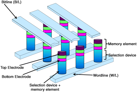
Figure 5.14 Cross-point memory with a memory cell integrated with a cell selector within a 4F2 footprint. This structure can be stacked in the third dimension. © IEEE. Reprinted with permission, from [7]
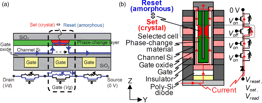
Figure 5.15 (a) Device structure and operation of PCM driven by Poly-Si MOS. © The Japan Society of Applied Physics. Reprinted with permission, from [117]. (b) Device structure and operation of VCCPCM. © IEEE. Reprinted with permission, from [120]
5.6 Applications
Phase Change Memory with its ability to achieve multiple resistance levels, fast access time, high endurance, scalability, CMOS compatibility and 3D stacking has the potential to be become the next generation memory technology for a variety of applications. In this section we will explore the use of phase change memory in two different applications namely, as storage class memories for conventional computing systems and as an electronic synaptic element for building brain-like systems for future computing applications.
5.6.1 PCM as a Storage Class Memory
Historically, device scaling has resulted in the benefit of both cost reduction and performance improvement for the computing systems and hence the unrelenting focus on the processor performance and logic device scaling was justified. However, due to power constraints in the processor and the diminishing returns of the performance advantage of logic device scaling, it is important to seek other areas of improvement through which we can continue to enhance the overall system performance. Of these, the most important one is the memory storage hierarchy. The major bottleneck today is the large gap in the access time between the magnetic HDD and the DRAM main memory [121,122]. There are no major technologies on track to improve the access times of the HDD in the near future. Because critical computing applications are becoming more data-centric than computer-centric, a high-performance, high-density, and low-cost nonvolatile memory technology whose access time falls between that of an HDD and the dynamic memory located near the processor would significantly improve the overall system performance while keeping the cost low. This class of memories is referred to as the Storage Class Memories (SCM) [121]. Figure 5.16 shows the different memory hierarchies that form a part of the computing system. The SCMs can fit in the memory hierarchy between the main memory and the HDD.
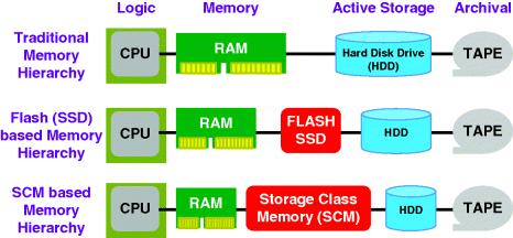
Figure 5.16 Memory hierarchy in computing systems. The performance gap between the main memory and the hard disk drive can be significantly reduced by using storage class memories in the memory hierarchy [140]
Of all the other emerging technologies, PCM is in the most advanced stages of meeting all the requirements for the SCM that companies are considering to include it in the memory hierarchy to improve the performance of their high-end systems [123]. The access time, endurance and retention properties of the PCM [124] are well within the requirements of the SCM. As compared to Flash, PCM can do in-place updates (it is bit-alterable) and there is no need to first erase a whole block before one can write new data. Instead of 105 (or even lower) write endurance cycles, PCM has more than 109 write endurance cycles. All these add up to reducing a lot of the overhead in the memory controller to keep track of where the written bits are, doing garbage collection, and wear leveling that is required for Flash. A prototype high-performance solid state drive using PCM [136] is shown to be 72–120% faster than Flash for small write and for all reads and incurs 20–51% less CPU overhead per IOP (Input Output Processor) for small requests. In another hybrid main memory system using phase change memory in conjunction with a small DRAM buffer [137] it was found that for a 16-core 8 GB DRAM baseline system, this hybrid PCM design reduces page faults by 5× and speeds up the system by 3×.
In addition, the major issues of having a 4F2 access device and reducing the programming current are also being addressed. Recently, there were demonstrations of several large scale Gb array demonstrations of PCM using 4F2 poly-Si diode [118,119]. If this trend in the technology improvement of PCM continues, then in the next few years we may be able to see commercial computing and mobile systems that contain PCM chips as a part of their memory hierarchy.
5.6.2 PCM as an Electronic Synapse
The ability to gradually program the cell into its SET or RESET state or in other words the ability to change the conductance of the device gradually makes PCM an excellent candidate to mimic the synaptic elements in the brain. Human brain predominantly consists of two main units, namely the neurons and the synapses that connect these neurons (Figure 5.17a). These synaptic elements have a certain behavior called Spike Timing Dependent Plasticity (STDP) wherein the conductance of the synaptic element changes based on the difference in the arrival time of the pulses or spikes from the post- and presynaptic neurons; that is, the conductance of the synapse increases when the prespike occurs before the post-spike and the conductance decreases when vice versa, as shown in Figure 5.17b. This particular behavior of the synapse is found to be one of the major factors that help in the process of learning and perception in brain [125]. PCM devices can be programmed in such a way that the pre- and postspike arriving at the two opposite terminals of the device can modulate the conductance of the device [126–128]. Thus PCM can act as an electronic synapse that connects neuron circuit elements (built with CMOS for instance) in a system architecture that closely resembles the brain. One implementation is to use a crossbar-like architecture that connects the different synaptic elements to the neuron circuits, with the top and bottom metal lines providing the pre- and postspike. Kuzum et al. [126] proposed a specific spiking scheme to translate the spike arriving timing relationship into PCM programming pulses. This enables the PCM to mimic the synaptic STDP behavior. The spiking scheme and the TEM cross-section of the nanoelectronic synapse used are shown in Figure 5.17c,d. Another pulsing scheme was also proposed in [127], where single pulses are used as opposed to multiple pulses as in Figure 5.17c to reduce complexity of neuron circuits and potentially energy consumption. The eventual goal is to build an array of synapses and neurons to emulate different learning functions. Another application example of PCM in cognitive computing was shown by Suri et al. [128]. A 2-PCM configuration was used in which the depression of the synapse is emulated by gradual SET of one cell, and potentiation is implemented by gradual SET in the other cell. Hence the energy consumption on the system level can be reduced since the RESET pulses are replaced by SET pulses, which consume less energy. Besides, this can be used when RESET process is abrupt due to device design or material composition required, given that gradual SET can be performed. However, this configuration occupies larger area than a one-cell synapse and requires a separate control to RESET both cells regularly while keeping the synaptic weight. Besides single synaptic device level experimental demonstrations, array level brain-like associative learning has also been experimentally implemented with phase change memory devices [129]. It was shown that for cognitive computing applications, resistance variations can be tolerated at the expense of energy consumption [130].
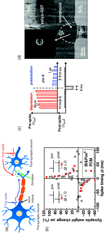
Figure 5.17 (a) A biological neuron and synapse. The synapse has the post- and prespikes applied on either side. © Journal of Neuroscience. Reprinted with permission, from [125]. (b) The asymmetric STDP curve for the synapse (both biological [125] and electronic [126]) showing the change in the conductance value with respect to the timing difference between the pre- and postspike. © American Chemical Society. Reprinted with permission, from [126]. (c) Pre- and postspikes that were used to program the electronics synapse [126]. The overlap of the two spikes at different time instants results in a different cell conductance due to the difference in the overall voltage difference across the cell. (d) TEM cross-section of the electronic synapse that is programmed in its lowest conductance (amorphous) state. Reprinted with permission from [126]. Copyright 2012 American Chemical Society
PCM technology has the promise to build human-scale intelligent systems which has not been possible so far due to lack of energy and area efficient hardware. Energy efficient artificial neural networks that can perform complex tasks with large amounts of inputs and variables can be made possible due to low energy consumption and nano-scale feature sizes of PCM technology. In a possible implementation, PCM devices can be deposited on top of CMOS neuron circuits. Several challenges such as process integration, RC delay, thermal disturbances and architectural problems should be addressed for such a configuration. Device models suitable for neuromorphic architectures are still needed for application-specific performance evaluations of these systems.
5.7 Future Outlook
The last decade has seen tremendous advances of the technology and fundamental research in phase change materials. Multi giga-bit phase change memory chips on par with conventional Flash technology were demonstrated in 20 nm technology [119]. Phase Change Memory is maturing from being a mere research topic and is now moving to large-scale manufacturing following the recent announcement [131] by Micron and Nokia where PCM multi-chip packages will be used in their smart phones to enable faster boot time, longer battery life, and better reliability. A number of industrial joint ventures such as Intel-Micron and IBM-Hynix have been formed to accelerate the PCM development for both mobile and high-end server market. Table 5.2 summarizes key PCM parameters that have been demonstrated and projected.
Table 5.2 Summary parameter table of Phase Change Memory
| Parameter | Demonstrated/projected | Value for the device in the chapter |
| Bottom electrode contact area | Demonstrated | 165 nm2 [119] |
| Projected1 | 2.5 nm2 [101] | |
| Feature size F | Demonstrated | 20 nm [119] |
| Projected | 8 nm [144] | |
| Cell size2 | Demonstrated | 4F2 [119] |
| Projected | 4F2 | |
| Density3 | Demonstrated | 59.5 Gb cm−2 [119] |
| Projected | 6.25 Tb cm−2 [119] (4 bit/cell) | |
| Read time | Demonstrated | 12 ns [145] |
| Projected | <10 ns [144] | |
| Write (reset) time | Demonstrated | 100 ns [145] |
| Projected | 400 ps [146] | |
| Write (Set) time | Demonstrated | 150 ns [143] |
| Projected | 500 ps [42] | |
| Read operation voltages | Demonstrated | 1.2 V [145] |
| Projected4 | <0.5 V [147] | |
| Write operation voltages | Demonstrated | 3 V [145] |
| Projected4 | <0.5 V [147] | |
| Reset current | Demonstrated | 90 μA [119] |
| Projected | <2 μA [92,101] | |
| Programming current density | Demonstrated | 10 MA cm−2 [7] |
| Projected4 | 3.3 MA cm−2 [147] | |
| Switching energy | Demonstrated | 6E-12 J bit−1 [145] |
| Projected5 | <1E-15 J bit−1 [92] | |
| Endurance | Demonstrated | 1E-12 [119] |
| Projected | 1E-15 [148] | |
| Retention | Demonstrated | >10 yr |
| Projected | >10 yr | |
| Binary throughput | Demonstrated | 40 MB s−1 [143] |
| Projected6 | 100 MB s−1 [148] | |
| The “Demonstrated” numbers are values from devices in multi-GB PCM chips. | ||
| The “Projected” numbers are values or estimates based on single device demonstrations. | ||
| 1The smallest active programming area demonstrated using a PCM device with CNT electrodes. | ||
| 2Including a diode-based cell selector device. | ||
| 3The numbers are based on a single device dimension. The effect of peripheral circuits and other interconnects are not included. | ||
| 4Based on GeTe/Sb2Te3 superlattice memory. | ||
| 5Estimated based on a minimum pulse width of 1 ns. | ||
| 6Based on the requirements of Storage Class Memories. | ||
In terms of the fundamental research, the resonant bonding phenomenon observed in the crystalline phase of phase change materials is an important factor that governs their unique properties in terms of reflectivity/resistivity change. Therefore, it is now possible to derive structure–property maps based on an understanding for which compositions resonance bonding can be expected in the crystalline state. Such maps are not only useful because they identify candidates for storage applications. More importantly, the understanding of the bonding characteristics contained in such data will provide insight into systematic property changes, which can help tailor materials for specific storage applications. The phase transition from the crystalline to the amorphous phase has traditionally been achieved by melt-quenching the phase change material. However, the recent demonstration of Interfacial PCM and other ultra-fast optical switching studies indicate that the phase transformation can be brought about by bond rearrangements at substantially reduced entropic losses. This can lead to the development of fast and efficient switching devices based on nano-structured materials that make use of this entropy controlled switching. The future PCM devices would see more of nano-structured phase change materials obtained via superlattice formation, dopant addition, or chemically synthesized nanoparticles. These provide an efficient way of tailoring some of the fundamental material properties such as crystallization time, crystallization temperature, melting temperature, and threshold field.
Understanding the electrical properties of sub-threshold conduction and threshold switching continues to be a topic of investigation as there is no consensus on the physical mechanism that governs these processes. It is important to understand these phenomena, especially as we approach device dimensions and material thicknesses that are close to the inter-trap distances. In terms of resistance drift, the constant debate continues as to whether the change in resistance with time is due to the structural relaxation of the decaying trap states or a mechanical stress release of the compressed programming volume. Understanding this drift process is a key to engineer materials and device structures that have minimal drift coefficient and to enable multi-level programming in phase change memories. However it is encouraging to see that, this problem of drift has been mitigated to some extent by using clever read out metrics that are inherently drift-tolerant, albeit comes with the cost of additional energy and area requirements.
In terms of device scaling, the recent demonstrations of carbon nanotube-based PCM devices, have given more confidence in that, the PCM technology will continue to scale even to a single-digit nanometer scale and that the programming power can be significantly reduced at such highly scaled devices as expected from continued scaling of the electrode area. But the question remains however as to whether it would be possible to build large arrays of phase change memory at such scaled dimensions, because the influence of the interconnects would then play a major role in determining the speed, power and reliability of the overall system [137]. The increasing wire delays as the technology scales down, electro-migration effects at higher current densities, reduction in the read/write margin for increasing wire resistances will demand a more rigorous device and interconnect co-optimization for cross-bar arrays in the sub-10 nm node [132]. Possible solutions also include using of wires with better conductivity and scalability (e.g., graphene and CNTs), memory arrays with smaller partition sizes, strapping the bitlines/wordlines with wider wires, and memory elements with larger resistance values and ratios.
The demonstration of 4F2 access devices for large arrays could lead to 3D stackable arrays in the future that form the basis of ultra high density phase change memory arrays. Achieving multi-bit, multi-layer phase change memory would be a key step in the large scale commercialization of PCM in the storage market. In addition to the nonvolatile memory applications, phase change memory has the potential to be used for neuromorphic applications as artificial synapses to emulate the learning behavior. Such brain-like systems are being contemplated for augmenting conventional computing because of the limitations of the traditional von Neumann architecture in terms of its energy efficiency in application areas such as performing cognitive operations. It is also possible to use phase change memories to perform accumulation operations in either optical or electrical domain, exploiting the gradual changes that take place in programming volume as one goes from the amorphous phase to the crystalline phase [133]. With a simple accumulator we can perform all the basic arithmetic processes of addition, subtraction, multiplication, and division while simultaneously storing the result at the same physical location.
It has almost been over four decades since the discovery of the switching effect in chalcogenides by Stanford Ovshinsky, but these materials still remain a mystery in terms of their fundamental understanding and new theories are developed every year and new applications are being proposed. One can only say that, with all that these materials have to offer to us, “There is plenty of room in the disorder.”
5.8 Summary
The field of phase change memory research has gained momentum in the last decade because of its interesting device and material properties that make them an excellent candidate for future nonvolatile memory applications. This chapter gives an overview of the basic device structure, the physical mechanisms underlying the various processes of phase change, the different device metrics that are important in evaluating the success of PCM technology and some of the possible future applications. There is however a vast body of literature in the field of phase-change materials research and its application in optical disk storage that are not covered in this chapter. We highlight some of the recent innovations in materials and device engineering that has enabled low power programming, ultimate device scaling and large-scale device integration.
Acknowledgments
This work is supported in part by the National Science Foundation (NSF, ECCS 0950305), Intel through the Global Research Collaboration (GRC) of the Semiconductor Research Corporation, the MSD Center of the Focus Center Research Program (FCRP), a Semiconductor Research Corporation subsidiary, and the member companies of the Non Volatile Memory Technology Research Initiative (NMTRI) at Stanford University. Collaborations with Prof. Kenneth Goodson (Stanford), Prof. Mehdi Asheghi (Stanford), Dr. Simone Raoux (IBM), Dr. Chung Lam (IBM), Dr. G.A.M. Hurkx (NXP), Dr. B.J. Bae (Samsung), and Dr. Delia Milliron (LBNL Molecular Foundry) are greatly appreciated. We thank the contributions of graduated students and post-doctoral researchers to this review: Dr. SangBum Kim, Dr. Marissa Caldwell, Dr. Duygu Kuzum, and Dr. Jiale Liang.
References
- 1. Ovshinsky, S.R. (1968) Reversible electrical switching phenomena in disordered structures. Physical Review Letters, 21, 1450.
- 2. Lai, S. (2003) Current status of the phase change memory and its future. Electron Devices Meeting, 2003. IEDM '03 Technical Digest. IEEE International, pp. 10.1.1–10.1.4.
- 3. Burr, G.W., Kurdi, B.N., Scott, J.C. et al. (2008) Overview of candidate device technologies for storage-class memory. IBM Journal of Research and Development, 52, 449–464.
- 4. Pirovano, A., Lacaita, A.L., Benvenuti, A. et al. (2003) Scaling analysis of phase-change memory technology. Electron Devices Meeting, 2003. IEDM '03 Technical Digest. IEEE International, pp. 29.6.1–29.6.4.
- 5. Burr, G.W., Breitwisch, M.J., Franceschini, M. et al. (2010) Phase change memory technology. Journal of Vacuum Science and Technology B, 28, 223.
- 6. Ielmini, D. (2008) Threshold switching mechanism by high-field energy gain in the hopping transport of chalcogenide glasses. Physical Review B, 78, 035308.
- 7. Wong, H.-S.P., Raoux, S., Kim, S. et al. (2010) Phase change memory. Proceedings of the IEEE, 98(12), 2201–2227.
- 8. Lankhorst, M.H.R., Ketelaars, B.W.S.M.M., and Wolters, R.A.M. (2005) Low-cost and nanoscale non-volatile memory concept for future silicon chips. Nature Materials, 4, 347–352.
- 9. Yamada, N., Kojima, R., Nishihara, T. et al. (2009) 100 GB rewritable triple-layer optical disk having Ge-Sb-Te films. Europ. Phase Change and Ovonic Science Symp, Aachen, Germany, pp. 23–28.
- 10. Raoux, S., Rettner, C.T., Jordan-Sweet, J.L. et al. (2007) Direct observation of amorphous to crystalline phase transitions in nanoparticle arrays of phase change materials. Journal of Applied Physics, 102, 094305–8.
- 11. Raoux, S., Cabrera, D., Devasia, A. et al. (2011) Influence of Dopants on the Crystallization Temperature, Crystal Structure, Resistance, and Threshold Field for Ge2Sb2Te5 and GeTe Phase Change Materials. European Phase Change and Ovonics Symposium.
- 12. Cheng, H.Y., Wu, J.Y., Cheek, R. et al. (2012) A Thermally Robust Phase Change Memory by Engineering the Ge/N Concentration in (Ge,N)xSbyTez Phase Change Material. Electron Devices Meeting, 2012. IEDM '12 Technical Digest. IEEE International, pp. 31.1.1–31.1.4.
- 13. Ielmini, D. and Zhang, Y. (2007) Analytical model for subthreshold conduction and threshold switching in chalcogenide-based memory devices. Journal of Applied Physics, 102, 054517-13.
- 14. Fugazza, D., Ielmini, D., Lavizzari, D.S., and Lacaita, A.L. (7–9 Dec. 2009) Distributed-Poole-Frenkel modeling of anomalous resistance scaling and fluctuations in phase-change memory (PCM) devices. Electron Devices Meeting (IEDM), 2009 IEEE International, pp. 1–4.
- 15. Krebs, D., Raoux, S., Rettner, C.T. et al. (2009) Threshold field of phase change memory materials measured using phase change bridge devices. Applied Physics Letters, 95, 082101.
- 16. Owen, A.E., Robertson, J.M., and Main, C. (1979) The threshold characteristics of chalcogenide-glass memory switches. Journal of Non-Crystalline Solids, 32, 29–52.
- 17. Adler, D., Henisch, H.K., and Mott, S.D. (1978) The mechanism of threshold switching in amorphous alloys. Reviews of Modern Physics, 50, 209–220.
- 18. Pirovano, A., Lacaita, A.L., Benvenuti, A. et al. (2004) Electronic switching in phase-change memories. Electron Devices, IEEE Transactions on, 51, 452–459.
- 19. Adler, D., Shur, M.S., Silver, M., and Ovshinsky, S.R. (1980) Threshold switching in chalcogenide glass thin films. Journal of Applied Physics, 51, 3289–3309.
- 20. Adler, D., Shur, M.S., Silver, M., and Ovshinsky, S.R. (1984) Reply to comment on threshold switching in chalcogenide glass thin films. Journal of Applied Physics, 56, 579–580.
- 21. Karpov, V.G., Kryukov, Y.A., Savransky, S.D., and Karpov, I.V. (2007) Nucleation switching in phase change memory. Applied Physics Letters, 90, 123504–123504-3.
- 22. Raoux, S., Cohen, G.M., Shelby, R.M. et al. (April 2010) Amorphization of crystalline phase change material by ion implantation. Mater. Res. Soc. Spring Meeting, San Francisco.
- 23. Pirovano, A., Lacaita, A.L., Pellizzer, F. et al. (2004) Low-field amorphous state resistance and threshold voltage drift in chalcogenide materials. Electron Devices, IEEE Transactions on, 51, 714–719.
- 24. Boniardi, M., Redaelli, A., Pirovano, A. et al. (2009) A physics-based model of electrical conduction decrease with time in amorphous Ge2Sb2Te5. Journal of Applied Physics, 105, 084506.
- 25. Ielmini, D., Lavizzari, S., Sharma, D., and Lacaita, A.L. (2008) Temperature acceleration of structural relaxation in amorphous Ge2Sb2Te5. Applied Physics Letters, 92, 193511.
- 26. Karpov, I.V., Mitra, M., Kau, D. et al. (2007) Fundamental drift of parameters in chalcogenide phase change memory. Journal of Applied Physiology, 102, 124503–124509.
- 27. Kim, S., Lee, B., Asheghi, M. et al. (2011) Resistance and threshold switching voltage drift behavior in phase-change memory and their temperature dependence at microsecond time scales studied using a micro-thermal stage. Transactions on Electron Devices, 58, 584–592.
- 28. Ielmini, D., Lavizzari, S., Sharma, D., and Lacaita, A.L. (10–12 Dec. 2007) Physical interpretation, modeling and impact on phase change memory (PCM) reliability of resistance drift due to chalcogenide structural relaxation. Electron Devices Meeting, 2007. IEDM 2007. IEEE International, pp. 939–942.
- 29. Mitra, M., Jung, Y., Gianola, D.S., and Agarwal, R. (2010) Extremely low drift of resistance and threshold voltage in amorphous phase change nanowire devices. Applied Physics Letters, 96, 222111–222113.
- 30. Rizzi, M., Spessot, A., Fantini, P., and Ielmini, D. (2011) Role of mechanical stress in the resistance drift of Ge2Sb2Te5 films and phase change memories. Applied Physics Letters, 99, 223513–223515.
- 31. Zhou, G.F., Borg, H.J., Rijpers, J.C.N., and Lankhorst, M. (2000) Crystallization behavior of phase change materials: comparison between nucleation- and growth-dominated crystallization. Optical Data Storage, 2000. Conference Digest, pp. 74–76.
- 32. Avrami, M. (1939) Kinetics of phase change. I general theory. Journal of Chemical Physics, 7(12), 1103–1112.
- 33. Bruns, G., Merkelbach, P., Schlockermann, C. et al. (2009) Nanosecond switching in GeTe phase change memory cells. Journal of Applied Physiology, 95, 043108.
- 34. Shimakawa, K. (2012) Dynamics of crystallization with fractal geometry: Extended KJMA approach in glasses. Physica Status Solidi (b), Special Issue: Phase-change memory: Science and applications, 249(10), 2024–2027.
- 35. Peng, C., Cheng, L., and Mansuripur, M. (1997) Experimental and theoretical investigations of laser-induced crystallization and amorphization in phase-change optical recording media. Journal of Applied Physiology, 82(9), 4183.
- 36. Senkader, S. and Wright, C.D. (2004) Models for phase-change of Ge2Sb2Te5 in optical and electrical memory devices. Journal of Applied Physiology, 95(2), 504–511.
- 37. Ahn, C., Lee, B., Jeyasingh, R.G.D. et al. (2011) Crystallization properties and their drift dependence in phase-change memory studied with a micro-thermal stage. Journal of Applied Physiology, 110, 114520.
- 38. Yamada, N. (2009) Phase change materials: science and applications, in: Development of Materials for Third Generation Optical Storage Media, Springer, Berlin.
- 39. Shportko, K., Kremers, S., Woda, M. et al. (2008) Resonant bonding in crystalline phase-change materials. Nature Materials, 7, 653–658.
- 40. Simpson, R.E., Fons, P., Kolobov, A.V. et al. (2011) Interfacial phase change memory. Nature Nanotechnology, 6, 501–505.
- 41. Lencer, D., Salinga, M., Grabowski, B. et al. (2008) A map for phase-change materials. Nature Materials, 7, 972–977.
- 42. Loke, D., Lee, T.H., Wang, W.J. et al. (2012) Breaking the speed limits of phase-change memory. Science, 336(6088), 1566–1569.
- 43. Wang, W.J., Loke, D., Law, L.T. et al. (2012) Engineering Grains of Ge2Sb2Te5 for Realizing Fast-Speed, Low-Power, and Low-Drift Phase-Change Memories with Further Multilevel Capabilities. Electron Devices Meeting, 2012. IEDM '12 Technical Digest. IEEE International, pp. 31.3.1–31.3.4.
- 44. Akola, J., Jones, R.O., Kohara, S. et al. (2009) Experimentally constrained density-functional calculations of the amorphous structure of the prototypical phase-change material Ge2Sb2Te5. Physical Review B-Condensed Matter, 80, 020201.
- 45. Matsunaga, T., Akola, J., Kohara, S. et al. (2011) From local structure to nanosecond recrystallization dynamics in AgInSbTe phase change materials. Nature Materials, 10, 129.
- 46. Kolobov, A.V., Krbal, M., Fons, P. et al. (2011) Distortion-triggered loss of long-range order in solids with bonding energy hierarchy. Nature Chemistry, 3, 311.
- 47. Fons, P., Osawa, H., Kolobov, A.V. et al. (2010) Photoassisted amorphization of the phase-change memory alloy Ge2Sb2Te5. Physical Review B-Condensed Matter, 82, 041203–041206.
- 48. Nam, S.-W., Chung, H.-S., Lo, Y.C. et al. (2012) Electrical wind force–driven and dislocation-templatedamorphization in phase-change nanowires. Science, 336(6088), 1561–1566.
- 49. Reifenberg, J., Pop, E., Gibby, A. et al. (2006) Multiphysics Modeling and Impact of Thermal Boundary Resistance in Phase Change Memory Devices. Thermal and Thermomechanical Phenomena in Electronics Systems, 2006. ITHERM '06. The Tenth Intersociety Conference on, May 30 2006–June 2 2006, pp. 106–113.
- 50. Risk, W.P., Rettner, C.T., and Raoux, S. (2008) In situ 3 omega techniques for measuring thermal conductivity of phase-change materials. Review of Scientific Instruments, 79, 14–19.
- 51. Reifenberg, J.P., Panzer, M.A., Kim, S. et al. (2007) Thickness and stoichiometry dependence of the thermal conductivity of GeSbTe films. Applied Physics Letters, 91, 111904-1–111904-3.
- 52. Reifenberg, J.P., Chang, K.W., Panzer, M.A. et al. (2010) Thermal boundary resistance measurements for phase-change memory devices. IEEE Electron Device Letters, 31, 56–58.
- 53. Lyeo, H.K., Cahill, D.G., Lee, B.S. et al. (2006) Thermal conductivity of phase-change material Ge2Sb2Te5. Applied Physics Letters, 89, 151904–151904-3.
- 54. Reifenberg, J.P. (Mar. 2010) Thermal phenomena in phase change memory. Ph.D dissertation: Stanford University.
- 55. Goodson, K.E. (2007) Ordering up the minimum thermal conductivity of solids. Science, 315, 342–343.
- 56. Li, Z., Lee, J., Reifenberg, J.P. et al. (2011) Grain boundaries, phase impurities, and anisotropic thermal conduction in phase change memory. IEEE Electron Device Letters, 32, 961–963.
- 57. Lee, J., Li, Z., Reifenberg, J.P. et al. (2011) Thermal conductivity anisotropy and grain structure in Ge2Sb2Te5 films. Journal of Applied Physiology, 109, 084902.
- 58. Small, E., Sadeghipour, S.M., Pileggi, L., and Asheghi, M. (2008) Thermal analyses of confined cell design for phase change random access memory (PCRAM). Thermal and Thermomechanical Phenomena in Electronic Systems, 2008. ITHERM 2008. 11th Intersociety Conference on, pp. 1046–1054.
- 59. Reifenberg, J.P., Kencke, D.L., and Goodson, K.E. (2008) The impact of thermal boundary resistance in phase-change memory devices. Electron Device Letters, IEE, 29, 1112–1114.
- 60. Sadeghipour, S.M., Pileggi, L., and Asheghi, M. (2006) Phase change random access memory, thermal analysis. Thermal and Thermomechanical Phenomena in Electronics Systems, 2006. ITHERM '06. The Tenth Intersociety Conference on, May 30 2006–June 2 2006, pp. 660–665.
- 61. Russo, U., Ielmini, D., Redaelli, A., and Lacaita, A.L. (2008) Modeling of programming and read performance in phase-change memories—part I: cell optimization and scaling. Electron Devices IEEE Transactions on, 55, 506–514.
- 62. Bozorg-Grayeli, E., Reifenberg, J.P., Panzer, M.A. et al. (2011) Temperature-dependent thermal properties of phase-change memory electrode materials. Electron Device Letters, IEEE, 32, 1281–1283.
- 63. Wu, J.Y., Breitwisch, M., Kim, S. et al. (2011) A low power phase change memory using thermally confined TaN/TiN bottom electrode. Electron Devices Meeting (IEDM), 2011 IEEE International, pp. 3.2.1–3.2.4.
- 64. Castro, D.T., Goux, L., Hurkx, G.A.M. et al. (2007) Evidence of the Thermo-Electric Thomson Effect and Influence on the Program Conditions and Cell Optimization in Phase-Change Memory Cells. Electron Devices Meeting, 2007. IEDM 2007. IEEE International, 10–12 Dec. 2007, pp. 315–318.
- 65. Suh, D.-S., Kim, C., Kim, K.H.P. et al. (2010) Thermoelectric heating of Ge2Sb2Te5 in phase change memory devices. Applied Physics Letters, 96(12), 123115.
- 66. Lee, J., Kodama, T., Won, Y. et al. (2012) Phase purity and the thermoelectric properties of Ge2Sb2Te5 Films down to 25nm Thickness. Applied Physics Letters, 112, 014902–014902-6.
- 67. Lee, J., Asheghi, M., and Goodson, K.E. (2012) Impact of thermoelectric phenomena on phase- change memory performance metrics and scaling. Nanotechnology, 23(20), 205201–205201-7.
- 68. Raoux, S., Burr, G.W., Breitwisch, M.J. et al. (2008) Phase-change random access memory: A scalable technology. IBM Journal of Research and Development, 52, 465–479.
- 69. Raoux, S., Shelby, R.M., Jordan-Sweet, J. et al. (2008) Phase change materials and their application to random access memory technology. Microelectronic Engineering, 85, 2330–2333.
- 70. Raoux, S. (2009) Scaling properties of phase change materials, in Phase Change Materials: Science and Applications (eds S. Raoux and M. Wuttig), Springer, Berlin, pp. 99–124.
- 71. Raoux, S., Cheng, H.-Y., Jordan-Sweet, J.L. et al. (2009) Influence of interfaces and doping on the crystallization temperature of GeSb. Applied Physics Letters, 94, 183114-3.
- 72. Wei, X., Shi, L., Chong, T.C. et al. (2007) Thickness-dependent nano-crystallization in Ge2Sb2Te5 and its effect on devices. Japanese Journal of Applied Physics, 46, 2211–2214.
- 73. Cheng, H.-Y., Raoux, S., Munoz, B., and Jordan-Sweet, J. (2009) Influence of interfaces on the crystallization characteristics of Ge2Sb2Te5. Non-volatile Memory Technol. Symp., Portland, OR.
- 74. Loke, D., Shi, L., Wang, W. et al. (2011) Ultrafast switching in nanoscale phase-change random access memory with superlattice-like structures. Nanotechnology, 22(25), 254019.
- 75. Lee, S.-H., Jung, Y., and Agarwal, R. (2007) Highly scalable non-volatile and ultra-low-power phase-change nanowire memory. Nature Nanotechnology, 2, 626–630.
- 76. Wautelet, M. (1991) Estimation of the variation of the melting temperature with the size of small particles, on the basis of a surface-phonon instability model. Journal of Physics D-Applied Physics, 24, 343–346.
- 77. Khonik, V.A., Kitagawa, K., and Morii, H. (2000) On the determination of the crystallization activation energy of metallic glasses. Journal of Applied Physiology, 87, 8440–8443.
- 78. Chong, T.C., Shi, L.P., Zhao, R. et al. (2006) Phase change random access memory cell with superlattice-like structure. Applied Physics Letters, 88, 122114.
- 79. Chen, Y., Li, D., Lukes, J.R. et al. (2005) Minimum superlattice thermal conductivity from molecular dynamics. Physical Review B-Condensed Matter, 72, 174302.
- 80. Tominaga, J., Fons, P., Kolobov, A. et al. (2008) Role of Ge switch in phase transition: approach using atomically controlled GeTe/Sb2Te3 superlattice. Japanese Journal of Applied Physics, 47, 5763–5766.
- 81. Wang, W.J., Loke, D., Shi, L.P. et al. (2012) Enabling universal memory by overcoming the contradictory speed and stability nature of phase-change materials. National Science Report, 2, 360.
- 82. Park, G.S., Kwon, J.H., Kim, M. et al. (2007) Crystalline and amorphous structures of Ge-Sb-Te nanoparticles. Journal of Applied Physics, 102, 70–72.
- 83. Choi, H.S., Seol, K.S., Takeuchi, K. et al. (2005) Sythesis and size-controlled Ge2Sb2Te5 nanoparticles. Japanese Journal of Applied Physics, 44, 7720–7722.
- 84. Zhang, Y., Wong, H.S.P., Raoux, S. et al. (2007) Phase change nanodot arrays fabricated using a self-assembly diblock copolymer approach. Applied Physics Letters, 91, 013104 3.
- 85. Zhang, Y., Raoux, S., Krebs, D. et al. (2008) Phase change nanodots patterning using a self-assembled polymer lithography and crystallization analysis. Journal of Applied Physics, 104, 20–22.
- 86. Milliron, D.J., Raoux, S., Shelby, R., and Jordan-Sweet, J. (2007) Solution-phase deposition and nanopatterning of GeSbSe phase-change materials. Nature Materials, 6, 352–356.
- 87. Caldwell, M.A., Raoux, S., Wang, R.Y. et al. (2010) Synthesis and size-dependent crystallization of colloidal germanium telluride nanoparticles. Journal of Materials Chemistry, 20, 1285–1291.
- 88. Kim, S., Bae, B.-J., Zhang, Y. et al. (2011) One-dimensional thickness scaling study of phase change material (Ge2Sb2Te5) using a Pseudo 3-terminal device. IEEE Transactions on Electron Devices, 58(5), 1483–1489.
- 89. Yu, D., Brittman, S., Lee, J.S. et al. (2008) Minimum voltage for threshold switching in nanoscale phase-change memory. Nano Letters, 8, 3429–3433.
- 90. Chen, Y.C., Rettner, C.T., Raoux, S. et al. (2006) Ultra-Thin Phase-Change Bridge Memory Device Using GeSb. Electron Devices Meeting, 2006. IEDM '06. International, pp. 1–4.
- 91. Krebs, D., Raoux, S., Rettner, C.T. et al. (2009) Characterization of phase change memory materials using phase change bridge devices. Journal of Applied Physics, 106, 90–92.
- 92. Xiong, F., Liao, A.D., Estrada, D., and Pop, E. (2011) Low-power switching of phase-change materials with carbon nanotube electrodes. Science, 332(6029), 568–570.
- 93. Sasago, Y., Kinoshita, M., Morikawa, T. et al. (2006) Cross-point phase change memory with 4F2 cell size driven by low-contact-resistivity poly-Si diode. VLSI Technology, 2009 Symposium on, 2006, pp. 24–25.
- 94. Ha, Y.H., Yi, J.H., Horii, H. et al. (2003) An edge contact type cell for Phase Change RAM featuring very low power consumption. VLSI Technology, 2003. Digest of Technical Papers. 2003 Symposium on, 2003, pp. 175–176.
- 95. Pellizzer, F., Pirovano, A., Ottogalli, F. et al. (2004) Novel m-trench phase-change memory cell for embedded and stand-alone non-volatile memory applications. VLSI Technology, 2004. Digest of Technical Papers. 2004 Symposium on, 2004, pp. 18–19.
- 96. Chen, W.S., Lee, C., Chao, D.S. et al. (2007) A Novel Cross-Spacer Phase Change Memory with Ultra-Small Lithography Independent Contact Area. Electron Devices Meeting, 2007. IEDM 2007. IEEE International, pp. 319–322.
- 97. Pirovano, A., Pellizzer, F., Tortorelli, I. et al. (2007) Self-aligned BC;Trench phase-change memory cell architecture for 90nm technology and beyond. Solid State Device Research Conference, 2007. ESSDERC 2007. 37th European, pp. 222–225.
- 98. Breitwisch, M., Nirschl, T., Chen, C.F. et al. (2007) Novel Lithography-Independent Pore Phase Change Memory. VLSI Technology, 2007 IEEE Symposium on, 2007, pp. 100–101.
- 99. Song, Y.J., Ryoo, K.C., Hwang, Y.N. et al. (2006) Highly Reliable 256Mb PRAM with Advanced Ring Contact Technology and Novel Encapsulating Technology. VLSI Technology, 2006. Digest of Technical Papers. 2006 Symposium on, 2006, pp. 118–119.
- 100. Im, D.H., Lee, J.I., Cho, S.L. et al. (2008) A unified 7.5nm dash-type confined cell for high performance PRAM device. Electron Devices Meeting, 2008. IEDM 2008. IEEE International, pp. 1–4.
- 101. Liang, J., Jeyasingh, R.G.D., Chen, H.-Y., and Wong, H.-S.P. (2012) An ultra-low reset current cross-point phase change memory with carbon nanotube electrodes. IEEE Transactions on Electron Devices, 59(4), 1155–1163.
- 102. Liu, B., Zhang, T., Xia, J.L. et al. (2004) Nitrogen-implanted Ge2Sb2Te5 film used as multilevel storage media for phase change random access memory. Semiconductor Science and Technology, 19, L61–L64.
- 103. Nirschl, T., Phipp, J.B., Happ, T.D. et al. (2007) Write Strategies for 2 and 4-bit Multi-Level Phase-Change Memory. Electron Devices Meeting, 2007. IEDM 2007. IEEE International, pp. 461–464.
- 104. Lai, Y.F., Feng, J., Qiao, B.W. et al. (2006) Stacked chalcogenide layers used as multi-state storage medium for phase change memory. Applied Physics a-Materials Science & Processing, 84, 21–25.
- 105. Rao, F., Song, Z., Wu, Z.M.L. et al. (2007) Multilevel data storage characteristics of phase change memory cell with doublelayer chalcogenide fims (Ge2Sb2Te5 and Sb2Te3). Japanese Journal of Applied Physics, 46, 80–82.
- 106. Zhang, Y., Feng, J., Zhang, Y. et al. (2007) Multi-bit storage in reset process of Phase-change Random Access Memory (PRAM). Physica Status Solidi-Rapid Research Letters, 1, R28–R30.
- 107. Yin, Y., Ota, K., Higano, N. et al. (2008) Multilevel storage in lateral top-heater phase-change memory. IEEE Electron Device Letters, 29, 876–878.
- 108. Oh, G.H., Park, Y.L., Lee, J.I. et al. (2009) Parallel multi-confined (PMC) cell technology for high density MLC PRAM. VLSI Technology, 2009 Symposium on, 2009, pp. 220–221.
- 109. Bedeschi, F., Fackenthal, R., Resta, C. et al. (2009) A bipolar-selected phase change memory featuring multi-level cell storage. IEEE Journal of Solid-State Circuits, 44, 217–227.
- 110. Nakayama, K., Takata, M., Kasai, T. et al. (2007) Pulse number control of electrical resistance for multi-level storage based on phase change. Journal of Physics D-Applied Physics, 40, 5061–5065.
- 111. Papandreou, N., Pozidis, H., Pantazi, A. et al. (2011) Programming Algorithms for Multilevel Phase-Change Memory. Proc. ISCAS, pp. 329–332.
- 112. Papandreou, N., Pozidis, H., Mittelholzer, T. et al. (2011) Drift-tolerant Multilevel Phase-Change Memory. Proc. IMW, pp. 147–150.
- 113. Hwang, Y.N., Um, C.Y., Lee, J.H. et al. (2010) MLC PRAM with SLC write-speed and robust read scheme. Proc. Symposium VLSI Circuits, pp. 201–202.
- 114. Lin, Y.Y., Chen, Y.C., Lee, F.M. et al. (2012) A Simple New Write Scheme for Low Latency Operation of Phase Change Memory. Symposium on VLSI Tech, Digest of Tech Papers, pp. 51–52.
- 115. Kau, D., Tang, S., Karpov, I.V. et al. (2009) A stackable cross point phase change memory. Electron Devices Meeting, 2009. IEDM '09 Technical Digest. IEEE International, pp. 617–620.
- 116. Gopalakrishnan, K., Shenoy, R.S., Rettner, C.T. et al. (2010) Highly-scalable novel access device based on Mixed Ionic Electronic conduction (MIEC) materials for high density phase change memory (PCM) arrays. VLSI Technology (VLSIT), 2010 Symposium on, 15–17 June 2010, pp. 205–206.
- 117. Sasago, Y., Kinoshita, M., Minemura, H. et al. (2011) Phase-change memory driven by poly-Si MOS transistor with low cost and high-programming gigabyte-per-second throughput. VLSI Technology (VLSIT), 2011 Symposium on, 14–16 June 2011, pp. 96–97.
- 118. Lee, S.H., Park, H.C., Kim, M.S. et al. (5–7 Dec. 2011) Highly productive PCRAM technology platform and full chip operation: Based on 4F2 (84nm pitch) cell scheme for 1Gb and beyond. Electron Devices Meeting (IEDM), 2011 IEEE International, pp. 3.3.1–3.3.4.
- 119. Kang, M.J., Park, T.J., Kwon, Y.W. et al. (5–7 Dec. 2011) PRAM cell technology and characterization in 20nm node size. Electron Devices Meeting (IEDM), 2011 IEEE International, pp. 3.1.1–3.1.4.
- 120. Kinoshita, M., Sasago, Y., Minemura, H. et al. (2012) Scalable 3-D vertical chain-cell-type phase-change memory with 4F2 poly-Si diodes. VLSI Technology (VLSIT), 2012 Symposium on, 12–14 June 2012, pp. 35–36.
- 121. Burr, G.W., Kurdi, B.N., Scott, J.C. et al. (2008) Overview of candidate device technologies for storage-class memory. IBM Journal of Research and Development, 52(4), 720–722.
- 122. Freitas, R.F. and Wilcke, W.W. (2008) Storage-class memory: The next storage system technology. IBM Journal of Research and Development, 52(4), 521–528.
- 123. Infoworld (2013) http://www.infoworld.com/d/hardware/ibm-turbocharge-more-servers-accelerators-364 (accessed 16 July 2013).
- 124. Ahn, Su Jin, Song, Yoonjong, Jeong, Hoon et al. (5–7 Dec. 2011) Reliability perspectives for high density PRAM manufacturing. Electron Devices Meeting (IEDM), 2011 IEEE International, pp. 12.6.1–12.6.4.
- 125. Bi, G.-Q. and Poo, M.-M. (1998) Synaptic modifications in cultured hippocampal neurons: dependence on spike timing and synaptic strength. Nature, 18, 10464–10472.
- 126. Kuzum, D., Jeyasingh, R., Lee, B., and Wong, H.-S.P. (2012) Nanoelectronic programmable synapses based on phase change. Nano Letters, 12(5), 2179–2186.
- 127. Kuzum, D., Jeyasingh, R., Yu, S., and Wong, H.-S.P. (2012) Low-energy robust neuromorphic computation using synaptic devices. IEEE Transactions on Electron Devices, 59(12), 3489–3494.
- 128. Suri, M., Bichler, O., Querlioz, D. et al. (5–7 Dec. 2011) Phase change memory as synapse for ultra-dense neuromorphic systems: Application to complex visual pattern extraction. Electron Devices Meeting (IEDM), 2011 IEEE International, pp. 4.4.1–4.4.4.
- 129. Eryilmaz, S.B., Kuzum, D., and Jeyasingh, R.G.D. et al. (9–11 Dec. 2013) Experimental demonstration of array-level learning with phase change synaptic devices. Electron Devices Meeting (IEDM). 2013 IEEE International, pp. 25.5.1–25.5.4.
- 130. Eryilmaz, S.B., Kuzum, D., and Jeyasingh, R.G.D. et al. (2014) Brain-like associative learning using a nanoscale nonvolatile phase change synaptic device array. Frontiers in Neuroscience, 8(205).
- 131. EE Times (2013) http://www.eetimes.com/design/memory-design/4403221/Micron-ships-phase-change-memory-for-Nokia-phones (accessed 16 July 2013).
- 132. Jiale, Liang, Yeh, S., Wong, S.S., and Wong, H.-S.P. (20–23 May 2012) Scaling Challenges for the Cross-Point Resistive Memory Array to Sub-10nm Node – An Interconnect Perspective. Memory Workshop (IMW), 2012 4th IEEE International, pp. 1–4.
- 133. Wright, C. David, Liu, Yanwei, Kohary, Krisztian I. et al. (2011) Arithmetic and biologically-inspired computing using phase-change materials. Advanced Materials, 23(30), 3408–3413.
- 134. Meyer, W. and Neldel, H. (1937) Fractal geometry and the Meyer–Neldel rule. Zeitung Technische Physik, 12, 588.
- 135. Collins, P.G., Arnold, M.S., and Avouris, P. (2001) Engineering carbon nanotubes and nanotube circuits using electrical breakdown. Science, 292(5517), 706–709.
- 136. Liang, J. and Wong, H.-S.P. (2010) Cross-point memory array without cell selectors – device characteristics and data storage pattern dependencies. IEEE Transactions on Electron Devices, 57(10), 2531–2538.
- 137. Liang, J., Yeh, S., Wong, S.S., and Wong, H.-S.P. (2013) Effect of wordline/bitline scaling on the performance, energy consumption, and reliability of cross-point memory array. ACM Journal on Emerging Technologies in Computing Systems (JETC), 9(1), 9:1–9:14, Article 9.
- 138. Akel, A., Caulfield, A.M., Mollov, T.I. et al. (2011) Onyx: a prototype phase change memory storage array. Proc. of the 3rd USENIX conference on Hot topics in storage and file systems, pp. 2.
- 139. Qureshi, M.K., Srinivasan, V., and Rivers, J.A. (2009) Scalable high performance main memory system using phase-change memory technology. ISCA '09 Proc. of the 36th annual international symposium on Computer architecture, pp. 24–33.
- 140. Kim, S., Lee, B., Asheghi, M. et al. (2–6 May 2010) Thermal disturbance and its impact on reliability of phase-change memory studied by the micro-thermal stage. Reliability Physics Symposium (IRPS), 2010 IEEE International, pp. 99–103.
- 141. Jeyasingh, R.G.D., Kuzum, D., and Wong, H.-S.P. (2011) Investigation of trap spacing for the amorphous state of phase-change memory devices. Electron Devices, IEEE Transactions on, 58(12), 4370–4376.
- 142. Freitas, R. (June (2009)) Storage Class Memory: Technology, Systems and Applications. 35th SIGMOD International Conference on Management of Data.
- 143. Choi, Y., Song, I., Park, M.-H. et al. (19–23 Feb. 2012) A 20nm 1.8V 8Gb PRAM with 40MB/s program bandwidth. Solid-State Circuits Conference Digest of Technical Papers (ISSCC), 2012 IEEE International, pp. 46, 48.
- 144. ITRS (2011) http://www.itrs.net/Links/2011ITRS/Home2011.htm, Emerging Research Devices, Table 2.
- 145. Sandre, G.De., Bettini, L., Pirola, A. et al. (2011) A 4 Mb LV MOS-selected embedded phase change memory in 90nm standard CMOS technology. Solid-State Circuits, IEEE Journal of, 46(1), 52, 63.
- 146. Wang, W.J., Shi, L.P., Zhao, R. et al. (2008) Fast phase transitions induced by picosecond electrical pulses on phase change memory cells. Applied Physics Letters, 93, 043121.
- 147. Takaura, N., Ohyanagi, T., Kitamura, M. et al. (2013) “Charge Injection Super-Lattice Phase Change Memory for Low Power and High Density Storage Device Applications.” paper T9.1, Symp. VLSI. Tech.
- 148. Ahn, D.H., Cho, S.L., Park, J.H. et al. (2012) “Key Metrics and Reliability Prospects for High Performance PRAM,” EPCOS.