
12
Memory Select Devices
An Chen
GLOBALFOUNDRIES Inc., USA
12.1 Introduction
With Flash memories approaching the scaling limit, some novel memory devices have emerged as potential candidates for Flash memory replacement, as shown in the taxonomy in Figure 12.1 [1]. Some promising examples include phase change memory (PCM), resistive random access memory (RRAM), spin transfer torque random access memory (STTRAM), and so on.
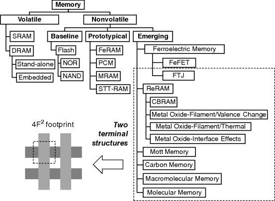
Figure 12.1 Memory taxonomy with two-terminal emerging memory devices highlighted. Inset shows a crossbar array layout with 4F2 device footprint
Many emerging nonvolatile memories (NVMs) have a simple two-terminal structure compatible with crossbar array architecture. Crossbar array layout enables device footprint as small as 4F2 (F: critical dimension of a technology node). By stacking up multiple layers of crossbar arrays [2,3] or building vertical 3D memory structures [4,5], even smaller footprint and higher memory density can be achieved. On the other hand, crossbar memory arrays also face challenges in device selection and isolation, which needs to be addressed by functional memory select devices.
12.2 Crossbar Array and Memory Select Devices
In crossbar arrays, memory devices are built at the junction between horizontal wordlines (WLs) and vertical bitlines (BLs), as shown in Figure 12.2. A device (e.g., Rj) is selected by applying voltages to its access lines. The unselected devices form large number of sneak paths in parallel with the selected path, which degrades the accessibility to the selected device. One example of these sneak paths is shown in Figure 12.2. The impact of the sneak paths on the reading and writing operations of crossbar arrays has been analyzed in numerous papers [6–14].
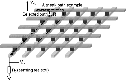
Figure 12.2 Illustration of a crossbar array with the selected current path (the dashed line) and an example of sneak paths (the dotted dashed line) highlighted
To reduce the impact of sneak paths, select devices need to be inserted at every junction in series with the memory elements. Most test chips of emerging memories use transistors as select devices in a 1-transistor-1-resistor (1T1R) configuration; however, the three-terminal structure and large footprint of transistors compromise the scaling advantages of crossbar arrays. Instead, two-terminal select devices are more compatible with crossbar arrays and 3D memories. Figure 12.3 illustrates all possible sneak paths in parallel with a selected device at junction (i,j) in a m × n array. Notice that leakage current through any sneak paths flows from WL to BL, BL to WL and WL to BL, that is, along any sneak paths there always exists a segment with reverse direction for current flow. Therefore, an asymmetrical device with significantly higher reverse resistance can help to reduce sneak current. Figure 12.3 also shows that multiple unselected devices share the voltage applied on a selected device, that is, unselected devices usually have lower bias than that of the selected device. This can also be ensured by proper bias of unselected WLs/BLs. So a nonlinear device with higher resistance at lower voltage can make sneak paths effectively more resistive and reduce sneak current. Therefore, both asymmetry and nonlinearity in device characteristics can help to reduce the impact of sneak paths in crossbar arrays.

Figure 12.3 An illustration of all possible sneak paths in parallel with a selected device R(i,j) in a m × n array
Functional select devices should provide either asymmetry or nonlinearity. Asymmetry is readily available in rectifying diodes. Nonlinearity can be introduced by non-ohmic transport mechanisms (e.g., tunneling) or some volatile switching phenomena (e.g., threshold switching). Figure 12.4 categorizes these memory select device options.
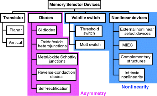
Figure 12.4 Taxonomy of memory select devices
To work for a given array size, select devices need to have sufficient difference between conductive state and blocking state, measured by resistance. This can be described by an ON/OFF ratio, which is the rectification ratio for diodes and the nonlinearity ratio for nonlinear devices. Select devices also need to provide sufficiently high current for the switching of the memory elements, so the maximum ON current is another key parameter. It is desirable that select devices are at least as scalable as the memory element to avoid compromising their scaling advantage. The key parameters of memory select devices are summarized in Table 12.1.
Table 12.1 Parameters of select devices
| Parameter | Explanations |
| ON/OFF ratio | Resistance ratio between ON and OFF state; affects array size |
| Maximum ON current | Needs to be sufficiently high for the switching of memory elements |
| Scalability | Needs to be as scalable as the memory elements. |
| Threshold voltage | The minimal voltage required to turn on the select devices. |
| Operation polarity | ON and OFF states in the same (unipolar) or opposite (bipolar) directions. |
| Switching speed | How fast select devices turn on and off affects the speed of memory. |
| Endurance | Select devices are turned on and off during both writing and reading operations and are therefore subject to stronger requirements on endurance. |
| Manufacturability | Compatibility with memory integration process, material stability, thermal budget, process variability, and so on. |
Some emerging memories (e.g., RRAM) require current control during switching to achieve stable performance. Transistors as select devices can provide active switching control via gate voltage (Vg). However, two-terminal select devices generally lack the capability to control switching current. Peripheral transistors outside the crossbar array may be used to control switching current; however, the effectiveness may be weakened by parasitic components.
Variability of select devices needs to be carefully controlled. For diode-type select devices, at least one side of a junction needs to have low or intermediate doping; otherwise, breakdown voltage would be too low. For a volume of 10 nm3, a doping concentration as high as 1018 cm−3 means just a single atom. In such highly scaled devices, random dopant fluctuation may cause large variation and affect diode functions. Diode scaling is also limited by the finite size of the depletion region [15]. It is estimated that there is a minimum length of ∼8 nm for Si diodes, due to the lateral depletion. Contact resistance constrains maximum ON current of all select devices and should be minimized. It is estimated that contact resistivity <10−7 Ω·cm2 is needed for functional select devices.
12.3 Memory Select Device Options
12.3.1 Transistors as Memory Select Devices
Transistors are probably the best select devices in terms of performance. Flash memory is a combination of memory element (charge storage in the floating gate) and select device (transistor) in one device. Although transistors have sufficient ON/OFF ratio and ON current, their three-terminal structure and large footprint are unsuitable for crossbar arrays and 3D memories. Transistor Vg controls the current flowing through the memory element during switching, which affects the switching properties of some memories, for example, RRAM. Transistor characteristics and scaling trend are well understood; therefore, their compatibility for future-generation memories can be better projected than other less mature select devices. Gate all around (GAA) FET structures are considered a promising solution to address some scaling challenges of transistors. The GAA structure can also be applied on vertical transistors and tunnel FET (TFET).
The major disadvantages of transistors as select devices are the >4F2 footprint of planar transistors and the high processing temperature that limits transistors in 3D stackable memories. Vertical transistors with 4F2 footprint have been explored but their feasibility is not yet proven [16,17]. In addition, the half-pitch dimension of vertical transistors is related to the thickness of the channel, gate dielectrics, and gate contact, which affects the scaling of vertical select transistors. 4F2 BJT-access RRAM was demonstrated in [18].
In 1T1R configuration transistor channel resistance needs to be significantly lower than the resistance of the memory element; otherwise, the effective memory window will be dominated by the transistor rather than the memory element. However, transistor resistance has increased steadily while half-pitch scales down. Therefore, at highly scaled nodes memory elements also need to have relatively high resistance to be functional in 1T1R configuration.
Due to these challenges, 1T1R does not appear competitive against 3D NAND. An alternative function of transistors could be access devices in the peripheral for a block of small crossbar array [3]. The peripheral transistors will control the access to the block and limit the voltage/current during switching. The memory elements inside of the array are connected to two-terminal select devices. Since peripheral transistors do not need to scale as aggressively as the memory element, transistor resistance can be reduced. However, the effectiveness of switching control by peripheral transistors depends on parasitic components.
12.3.2 Diodes as Memory Select Devices
Diode select devices have the advantage in scalability but still face the challenges in ON/OFF ratio and maximum ON current [2,19,20]. Silicon diodes require high processing temperature and therefore low-temperature oxide-based diodes have been actively explored as alternatives. Regular diodes only work for unipolar switching devices (i.e., set and reset in the same voltage polarity direction). For bipolar switching memories (i.e., set and reset in the opposite directions), reverse-conduction diodes (e.g., Zener diode, BARITT diode, etc.) are in principle possible solutions; however little progress has been made in reverse-conduction diodes for memory select devices.
12.3.2.1 Silicon Diodes
Both single-crystal Si [21] and poly-Si diodes [22–24] have been developed as a select device for PCM arrays. To operate PCM with diode selectors, diodes need to provide ON-current density above 8 MA/cm2 and OFF-current density below 100 A/cm2. To provide such a high ON-current density, the contact resistivity needs to be reduced to <10−7 Ω·cm2. By engineering the metal electrodes and electrode-Si interface, total contact resistivity of top and bottom electrodes was reduced to 3.5 × 10⁻⁸ Ω·cm2 [22]. To minimize the OFF-current density, impurity concentration at junction needs to be reduced, which is achieved with an undoped Si layer between p- and n-layers [22]. A short-time annealing technique was developed to further reduce the OFF-current density and enlarge the ON/OFF ratio. Poly-Si technology can achieve ON-current density of 107 A/cm2 (at ∼1.8 V), OFF-current density of 10−1 A/cm2 (at ∼−1.5 V), that is, ON/OFF ratio of 108. The ideality factor is 2.2. It is believed that Si diode can be scaled beyond 20 or 10 nm. Poly-Si diode select devices have been integrated in PCM crossbar arrays [22], 3D vertical chain-cell type PCM [23], and a 1 Gb PCM test chip [24]. A major challenge of Si diodes is the high processing temperature (above 1000 °C) required to crystallize Si to reduce contact resistivity and OFF-current.
12.3.2.2 Oxide Heterojunction Diodes
Heterojunction diodes can be built using semiconducting oxides deposited at relatively low temperature, for example, 200–300 °C [25]. The rectifying oxide heterojunctions can be utilized as select devices, especially for oxide-based RRAM memory elements [25–28]. A p-NiOx/n-TiOx diode has demonstrated a rectification ratio of 105 at ±3 V, ON current density of 5 × 10³ A/cm2 (at ∼2.5 V), and ideality factor of 4.3 [25]. It was integrated with NOx-based RRAM elements to form 1D1R memory device. A p-CuOx/n-InZnOx diode achieved higher ON current density of 104 A/cm2 (at ∼1.3 V). It was integrated with NiOx RRAM in a two-layer 8 × 8 crossbar array [26,27] and with Al2O3 antifuse in a one-time programmable (OTP) memory [28]. Oxide p-n heterojunction was also demonstrated in p-ZnO·Rh2O3/n-InGaZnO4 and achieved on/off ratio of 103 (at ±5 V), ideality factor of ∼2.3, and threshold voltage of 2.1 V [29]. Si substrates can be used as a part of heterojunction diodes as demonstrated in n-ZnO/p-Si [30] and n-Ge-nanowire/p-Si [31]. The ON current of oxide-based heterojunction diodes is often limited by both contact resistance and density of states of the oxide materials.
12.3.2.3 Metal/Oxide Schottky Diodes
Metal/oxide Schottky diodes can also work as memory select devices [32–37]. In a TiOx-based diode with (In,Sn)2O3 (ITO) and Pt as electrodes, temperature-dependent current–voltage (I-V) characteristics confirms that Schottky barrier of ∼0.55 eV forms at the TiOx/Pt interface [32]. The rectification ratio is ∼1.6 × 10⁴ at ±1 V. ON current of ∼100 mA (at ∼1.5 V) is provided through a diode area of 7500 μm2, which corresponds to a low ON current density of ∼13 A/cm2. A Pt/TiO2/Ti diode with Pt as the Schottky contact and Ti the ohmic contact achieved rectification ratio of 107–109 at ±1 V, although ON current remains low at <10 A/cm2 (for an area of 60 000 μm2) [33]. Another demonstration of Pt/TiO2/Ti Schottky diodes showed rectification ratio of ∼2.4 × 10⁶ at ±2 V and ON current density of ∼3 × 10⁵ A/cm2 at 2 V on a 4 μm2 area [34]. Measurement showed that diode current density increases with decreasing area, indicating that current is not uniform across the diode area, which may be explained by edge leakage. Consequently, higher ON current density values can be obtained at smaller diode sizes. An Ag/n-ZnO Schottky diode with non-alloyed Ti/Au ohmic contact demonstrated a rectification ratio of 105 and forward current density over 104 A/cm2 at 2 V [35]. A rectifying Ti/TiO2/Pt diode was found to transition into a resistive switching device after a strong forming process, which is attributed to the destruction of the interface Schottky barrier by conductive filaments [36]. Similarly, a Pt/TiOx/Pt was also shown to behave as a switchable rectifier [37,38]. The coexistence of rectifying and switching behaviors in oxide diodes manifests the complexity of these material systems, which may cause reliability concerns. In addition to oxide Schottky diodes, Si Schottky diodes are also utilized as select devices, for example, Al/p-Si [39].
Figure 12.5 compares the forward versus reverse current density of some of the diodes discussed above [22,25,26,29,32,33,36,38]. Most diode select devices still cannot reach the ON current density target of 1 MA/cm2 marked in the figure. The diagonal direction dashed lines represent rectification ratio (e.g., 1, 104, and 108). Many diode devices can achieve rectification ratio above 104 at ±1 V. Rectification ratio is clearly lower at lower voltage (±0.5 V) because forward current decreases from 1.0 to 0.5 V and reverse current only changes slightly. Notice that the forward current density of some diodes changes much less than the exponential dependence between 1.0 and 0.5 V. This is because the forward current of these diodes is already limited by contact resistance at 0.5–1.0 V and deviates from the exponential diode I-V characteristics.
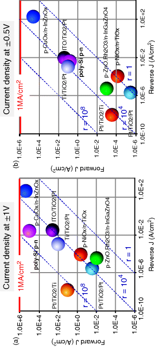
Figure 12.5 Comparison of diode select devices based on forward and reverse current density measured at (a) ±1 V and (b) ±0.5 V [References: 22,25,26,29,32,33,36,38]
Table 12.2 summarizes the processing temperature and ideality factors of some diode select devices discussed above. Low processing temperature is one of their major advantages.
Table 12.2 Summary of the processing temperature and ideality factor of some diode select devices
| Diodes | Processing temperature (°C) | Ideality factor, n | Ref. |
| p-NiOx/n-TiOx | <300 | 4.3 | 25 |
| p-CuOx/n-InZnOx | Room temperature | — | 27 |
| p-ZnO·Rh2O3/n-InGaZnO4 | Room temperature | 2.3 | 29 |
| Pt/TiO2/Ti | 250 | 1.02 | 33 |
| ITO/TiO2/Pt | 250 | — | 32 |
| Poly-Si p-n | >1000 | 2.2 | 22 |
12.3.2.4 Self-rectifying Resistive Switching Memories
Some RRAM devices are found to be self-rectifying, which may enable crossbar memory arrays without external select devices. In a RRAM device made from ZrO2 doped with Au nano-crystals, the low resistance state (LRS) exhibits asymmetrical characteristics with a rectification ratio of 102–103 measured at 0.5 V [40]. The self-rectification property is attributed to the Au/ZrO2 interface, while the resistive switching is explained by the formation of conductive filaments inside of ZrO2. A RRAM device with Al/PCMO interface was shown to be rectifying in LRS with a rectification ratio of ∼102 and symmetrical in high resistance state (HRS) [41]. The device was scaled down to 50 nm diameter and achieved endurance of 105 cycles for reading (0.5 V, 10 μs) and 104 cycles for writing (±7 V, 10/1 μs). A unipolar NiSi/HfOx/TiN RRAM device was also found to be rectifying in LRS with a rectification ratio of ∼103 at ±1 V due to the Schottky barrier at the NiSi/HfOx interface [42]. When heavily doped Si was used as one electrode for HfOx RRAM, self-rectifying unipolar resistive switching characteristics were observed on n+-Si but not on p+-Si [43,44]. Similar self-rectifying unipolar resistive switching characteristics were also reported on Ni/AlOx/n+-Si [39]. A bipolar Ni/TiO2/HfO2/Ni resistive switch exhibits rectifying characteristics in LRS, which was explained by the asymmetric tunnel barrier at the TiO2/HfO2 interface [45]. A Cu/α-Si/WO3/Pt device shows rectifying behavior in LRS with rectification ratio of 102 at ±0.75 V, which was attributed to the interface between the conductive filament in WO3 and the α-Si layer [46]. In a conductive-bridge RAM (CBRAM) with Cu/SiO2/n+-Si structure, it was found that the deposition of Cu on the n+-Si electrode results in the formation of a Schottky interface with a potential barrier of 0.65–0.75 eV [47]. Similar behavior was also reported in an Ag/α-Si-based CBRAM [48].
Most of the self-rectification is due to the Schottky contact between a metal electrode and the oxides/filaments. Self-rectifying memory devices could simplify the design and fabrication of crossbar arrays, especially in 3D vertical crossbar arrays. However, the combination of rectification and switching characteristics in one structure may also complicate the performance optimization of both the memory and select devices.
Some key parameters (e.g., rectification ratio, ON-state current) of reported rectifying diode select devices are summarized in Table 12.3.
Table 12.3 Key parameters of some reported rectifying diode select devices
| Rectifying diodes for select devices (only compatible with unipolar memory devices) | ||||||
| Device types | Materials | Sizea | Rectification ratio | Von b | Ion (Jon) |
Ref. |
| pn diodes | Single-crystal Si | 90 nm | 107–108 (at ±1 V) |
1.8 V | 1.8 mA 2.8 × 10⁷ A/cm2 |
21 |
| Poly-crystal Si | 80 nm | >106 (at ±2 V) |
2.0 V | 0.5 mA 8 × 10⁶ A/cm2 |
22 | |
| Schottky diodes | Ag/n-ZnO | — | ∼3 × 10⁵ (at ±2 V) |
2.0 V | — 1 × 10⁴ A/cm2 |
35 |
| Pt/TiO2 | 6 × 104 μm2 | 109 (at ±1 V) |
1.0 V | 6 mA 1 × 101 A/cm2 |
33 | |
| ITO/TiO2 | 7.5 × 103 μm2 | 3 × 10⁴ (at ±1 V) |
1.0 V | 30 mA 4 × 10² A/cm2 |
32 | |
| Pt/TiO2 | 2 × 2 μm2 | 2.4 × 10⁶ (at ±2 V) |
2.0 V | 10 mA 3 × 10⁵ A/cm2 |
34 | |
| Pt/TiO2 | — | 5 × 10⁵ (at ±2 V) |
2.0 V | — 5 × 10² A/cm2 |
36 | |
| Heterojunction diodes | n-ZnO/p-Si | 100 μm | 103 | 3.0 V | 25 mA 2.5 × 10² A/cm2 |
30 |
| p-CuOx/n-InZnOx | 0.5 × 0.5 μm2 | 3 × 10⁴ (at ±1 V) |
1.0 V | 0.15 mA 6 × 10⁴ A/cm2 |
28 | |
| p-NiOx/n-TiOx | 30 × 30 μm2 | 5 × 10⁵ (at ±2 V) |
2.0 V | 1.8 mA 2 × 10² A/cm2 |
25–27 | |
| p-ZnO·Rh2O3/n-InGaZnO4 | 500 × 500 μm2 | 2.5 × 10² (at ±1 V) |
1.0 V | 18 μA 7.2 × 10⁻³ A/cm2 |
29 | |
| Self-rectifying memory devices | Au/Au-nc:ZrO2 | 600 × 600 μm2 | 1 × 10³ (at ±1 V) |
1.0 V | 0.6 mA 1.7 × 10⁻¹ A/cm2 |
40 |
| Al/Pr0.7Ca0.3MnO3 | — | ∼80 (at ±3 V) |
3.0 V | ∼0.8 mA — |
41 | |
| Ni/HfOx/n+-Si | 7850 μm2 | 7 × 10³ (at ±0.8 V) |
0.8 V | 0.2 mA 2.6 A/cm2 |
43 | |
| Ni/AlOx/n+-Si | — | 4 × 10³ (at ±1 V) |
1.0 V | ∼1.5 mA — |
44 | |
| α-Si/WO3 | — | 102 (at ±2 V) |
2.0 V | ∼0.15 mA — |
46 | |
| Ag/α-Si | 100 × 100 nm2 | 106 (at ±0.5 V) |
0.5 V | 4 nA 4 × 101 A/cm2 |
48 | |
| aSize is diameter (d) or area (A). If not specified in the paper, device is assumed to be circular, that is, A = π(d/2)2. | ||||||
| bVon is where the forward current Ion is measured. | ||||||
12.3.3 Volatile Switches as Memory Select Devices
Volatile resistive switching devices can also be utilized as memory select devices. They provide access to a selected memory element in their ON state and block sneak paths in OFF state. The volatile switching characteristics allow them to be switched quickly between ON and OFF states.
12.3.3.1 Threshold Switches
In chalcogenide materials, a volatile threshold switching process occurs before stable nonvolatile memory switching is triggered. It was reported that chalcogenide-based threshold switches could be used as access devices in PCM arrays [49]. Niobium oxide is found to possess both memory switching and threshold switching properties at different compositions. Pt/NbO2−x/Pt threshold switching device becomes conductive above a threshold voltage (Vth) and falls back to high-resistance state below a hold voltage (Vhold) [50]. The threshold switching property remains stable up to 160 °C. By combining memory switching property of Nb2O5−x and threshold switching of NbO2−x, a hybrid memory (W/bi-layer-NbOx/Pt) was demonstrated in a 1 kb array [50]. In Si-As-Te ternary alloy, the composition (controlled by the sputtering power during deposition) determines the emergence of threshold switching [51]. Both Vth and Vhold vary with composition, which may provide a method to optimize the selector operation window. Functional 1-selector-1-resistor (1S1R) memory device with SiAsTe-based threshold switch selector and TiOx-based RRAM was demonstrated experimentally. Another threshold switch device based on AsTeGeSiN was shown to be scalable to 30 nm with current density exceeding 10 MA/cm2 and endurance over 108 cycles [52]. It was demonstrated as a functional select device for TaOx-based RRAM devices. NiOx was found to change from nonvolatile switching to threshold switching at higher oxygen concentration [53], which could be utilized to build all-NiOx memory devices with the select device and memory element both made from NiOx with different compositions [54].
12.3.3.2 Mott Transition Switches
Metal–insulator transition (MIT or Mott transition) induces several orders of magnitudes change of resistance in Mott materials [55], which could be utilized in memory select devices. A well-known Mott material is vanadium oxide (VOx) with typical transition temperature around 67 °C. It is believed that the intrinsic switching speed of VOx is below tens of ns or even sub-ns. The feasibility of VO2-based select devices is demonstrated by integrating a Pt/VO2/Pt device with NiOx-based RRAM [56]. Resistance of the VO2 select device can be switched over three orders of magnitudes with Vth of 0.6 V and Vhold of 0.4 V. The 1S1R memory device can be switched within tens of ns. Another demonstration of Pt/VO2/Pt select device achieved switching speed <20 ns, ON current of ∼1 MA/cm2, and Vth of 0.35 V, although the ON/OFF ratio is relative low (∼50) [57]. A functional 1S1R memory structure is demonstrated by integrating the VO2-switch with ZrOx/HfOx bipolar RRAM devices. Both threshold switching and memory switching have been observed in VOx, depending on O content [58]. A key challenge of VO2-based select devices is the low operation temperature. Mott materials with higher transition temperatures need to be found to provide feasible select device options [59].
12.3.4 Nonlinearity for Device Selection
As discussed earlier, nonlinearity improves the accessibility to a selected device by making unselected devices effectively more resistive via the voltage-dependent resistance.
12.3.4.1 Nonlinear Memory Select Devices
Nonlinearity can be easily achieved with non-ohmic transport mechanisms, for example, tunneling [3]. A Ni/TiO2/Ni device shows nearly symmetrical exponential I-V characteristics with six orders of magnitude of current change for voltage swing from 0 V to ±2 V [60]. It is integrated with HfO2-RRAM to demonstrate a 1S1R memory structure. Another TiO2-based nonlinear selector uses Pt/TiO2/TiN structure and is integrated with bi-layer Pt/TiO2−x/TiO2/W RRAM for a functional memory device [61]. A so-called “varistor” select device uses a 4 nm TiO2 layer sandwiched between two 10 nm TaOx layers and achieves 104 resistance difference between 1.5 and 0.75 V [62]. It was found that the substitution of Ti4+ in TiO2 by Ta5+ ions increases the conductivity of the initially insulating TiO2 layer. The ON current of nonlinear select devices can be modulated by oxide thickness and oxidation conditions. Some papers attributed the exponential I-V dependence to Schottky barriers at the metal/oxide interface; however, it did not explain why a back to back Schottky diodes can provide high ON current [60,61]. A more plausible explanation is the tunneling-based transport mechanisms in these oxide materials [62]. Temperature-dependent transport characterization would help to identify the actual mechanisms. Another possible mechanism for symmetrical exponential I-V characteristics in a back to back diode structure is provided in a n+/p/n+ poly-Si device model, where the middle p-layer is fully depleted and a drain induced barrier lowering (DIBL) effect causes exponential current increase with applied voltage [63].
12.3.4.2 Mixed Ionic Electronic Conduction Devices
A so-called mixed ionic electronic conduction (MIEC) device is developed as select devices for PCM [64–67]. The device is made from Cu-containing MIEC materials sandwiched between an inert top electrode (TE; e.g., TiN, W) and a bottom electrode (BE). Negative voltage applied on TE pulls Cu+ in MIEC away from the BE and create vacancies near BE. The hole and vacancy concentrations depend exponentially on the applied voltage. Symmetrical diode-like I-V characteristics can be achieved with two inert electrodes. Large fraction of mobile Cu+ enables high current density exceeding tens of MA/cm2 [64]. For example, a 40 nm MIEC device is able to provide a current >200 μA, that is, a current density >15 MA/cm2. The device selection capability of MIEC for large array is characterized by the voltage margin (Vm) between the positive and negative voltages measured at certain current level (e.g., 10 nA). It was shown that Vm increases with decreasing device size [64]. Endurance above 108 cycles has been demonstrated on MIEC devices in small arrays [65]. The failure mechanism was attributed to the accumulation of Cu near the TE, which was also found curable by thermal annealing. Endurance of MIEC increases exponentially with decreasing current and is independent of device sizes. The MIEC select devices were also integrated with PCM in a 512 kb testing array using 180 nm CMOS process and achieved 100% yield [66]. Electrode optimization plays critical roles in the yield improvement. It was demonstrated that MIEC devices tolerate processing temperature up to 500 °C and can be fabricated with manufacturing-level single-target sputter deposition. The scalability of MIEC select devices was tested to below 30 nm in diameter and below 12 nm in thickness [67]. An integrated MIEC-PCM memory device can be switched at the speed of 15 ns and read within 1 μs at typical reading current (∼5 μA).
12.3.4.3 Complementary Resistive Switch
A complementary resistive switch (CRS) provides a self-selecting memory by connecting two bipolar RRAM devices anti-serially [68]. It may be considered a “constructed nonlinearity” with re-defined logic states and operations. Both states “0” and “1” have high resistance in CSR, which helps to minimize leakage through sneak paths. In either state, one of the two RRAMs is in LRS and the other in HRS. When reading a “1” state, the HRS device is switched to LRS and both devices end up in LRS. When reading a “0” state, no switching occurs and CSR remains in HRS. Notice that the reading operation is destructive, which may degrade the overall endurance of CRS. A non-destructive readout method based on capacitive voltage divider was also proposed [69]. CRS has been demonstrated in different resistive switching devices, for example, Cu/SiO2/Pt bipolar resistive switches [70], amorphous carbon-based RRAM [71], TaOx–based RRAM [72–74], multi-layer TiOx device [75], HfOx RRAM [76], ZrOx/HfOx bi-layer RRAM [77], Cu/TaO2 atomic switch [78], Nb2O5−x/NbOy RRAM [79], and so on.
An important issue with CRS is the “ON window.” For CRS built from devices with asymmetric I-V curve, there will be no stable ON state if the asymmetry is so large that Vreset < Vset/2. A potential solution is to use series resistors to make the I-V curves symmetric. For RRAM based on valence change mechanism (VCM), CSR on-window may also be engineered by changing oxygen content and oxide thickness [75]. It was also suggested that hetero-devices (two different RRAM devices connected anti-serially) can be used to control the operation voltages of CSR [80]. In spite of these promising results of CRS, some critical challenges still remain for CRS. In-depth understanding of the HRS/LRS → LRS/LRS → LRS/HRS transitions for different materials is needed. Destructive reading method requires RRAM devices with good write endurance, since every read operation of CRS also involves a write operation. The operation voltage of CRS is also larger than that of single devices. The feasibility of CRS for crossbar arrays depends on solutions to these challenges.
12.3.4.4 Intrinsic Nonlinearity in Memory Device Characteristics
Nonlinear I-V characteristics may also be an intrinsic property of some resistive switching devices [81]. A tunneling oxide layer can be intentionally built in a RRAM device to provide nonlinearity I-V dependence. A TiOx-RRAM device is combined with different tunnel oxides, HfOx, ZrOx, or AlOx [82]. Appropriately chosen tunneling oxide layer not only provide built-in nonlinearity but also assist resistive switching process. In a TiOx/Ta2O5 bi-layer RRAM device, the nonlinearity and resistive switching characteristics can be modulated by processing conditions, which may enable a self-selecting crossbar array [83]. It was reported that a 64 Mb multi-layer RRAM array was fabricated with 0.13 μm CMOS process based on an oxide stack with an insulating oxide layer on top of a conductive oxide layer [84]. The insulating oxide provides variable tunnel barrier height and nonlinear characteristics.
Similar to the self-rectifying characteristics, intrinsic nonlinearity in resistive switching memories could simplify processing and enable really compact memory design. However, the interaction between the resistive switching mechanism and tunneling mechanism may also complicate the optimization of both properties.
The key parameters of some reported volatile switch and nonlinear select devices are summarized in Table 12.4.
Table 12.4 Key parameters of some reported volatile switch and nonlinear select devices
| Volatile switch select devices (compatible with both bipolar and unipolar memory devices) | ||||||||
| Device types | Materials | Sizea | On/off ratio | Vth b | Ion c (Jon) |
Vhold d | Ioff (Joff) |
Ref. |
| Threshold switch | Pt/NbO2−x/Pt | 250 nm | >10 (at ±1.5 V) |
∼1.6 V | >1 mA >4 × 10⁶ A/cm2 |
∼1.3 V | ∼0.1 mA (at 1.4 V) ∼4 × 10⁵ A/cm2 |
50 |
| Si-As-Tee | — | >102 (at ±1.0 V) |
1–2 V | >5 mA — |
0.5–1 V | ∼50 μA (at 1.0 V) - |
51 | |
| Ti/AsTeGeSiN/Ti | 30 nm | >25 (at ±1.5 V) |
∼1.75 V | >0.1 mA >1 × 10⁷ A/cm2 |
∼1.4–1.5 V | ∼4 μA (at 1.5 V) ∼4 × 10⁵ A/cm2 |
52 | |
| Pt/NiO/Ptf | 30 × 30 μm2 | >10 (at ±1.75 V) |
∼1.8 V | >50 mA >6 × 10³ A/cm2 |
∼1.6 V | ∼5 mA (at 1.75 V) ∼6 × 10² A/cm2 |
54 | |
| Mott transition | Pt/VO2/Pt | — | ∼300 (at 0.5 V) |
∼0.7 V | ∼10 mA — |
∼0.25 V | ∼30 μA (at 0.5 V) — |
56 |
| Pt/VO2/Pt | 250 nm | >75 (at ±0.3 V) |
0.35–0.4 V | >3 mA >6 × 10⁶ A/cm2 |
∼0.2 V | ∼40 μA (at 0.3 V) ∼8 × 10⁴ A/cm2 |
57 | |
| Nonlinear select devices (compatible with both bipolar and unipolar memory devices) | ||||||||
| Device types | Materials | Sizea | Nonlinearity ratiog | Full V | I(V) J(V) |
Half V | I(V/2) J(V/2) |
Ref. |
| Nonlinear MIM select devices | Ni/TiO2/Ni | 104 μm2 | >102 (at 2/1 V) |
2 V | (4–40) × 10−6 A (4–40) × 10−2 A/cm2 |
1 V | (4–8) × 10−8 A (4–8) × 10−4 A/cm2 |
60 |
| Pt/TiO2/TiN | 0.049 μm2 | ∼102 (at 2/1 V) |
2 V | (1–15) μA (2–30) × 103 A/cm2 |
1 V | (2.5–10) × 10−8 A (5–20) × 101 A/cm2 |
61 | |
| Pt/TaOx/TiO2/TaOx/Pt | 250 nm | ∼103 (at 2/1 V) |
2 V | ∼1 × 10⁻² A ∼2 × 10⁷ A/cm2 |
1 V | ∼1 × 10⁻⁵ A ∼2 × 10⁴ A/cm2 |
62 | |
| MIECh | Cu-containing material | <30 nm | >104 (at 1.0/0.5 V) |
1 V | >10−6 A >1.4 × 10⁵ A/cm2 |
0.5 V | ∼5 × 10⁻¹¹ A ∼7 A/cm2 |
67 |
| aSize is diameter (d) or area (A). If not specified in the paper, device is assumed to be circular, that is, A = π(d/2)2. | ||||||||
| bThreshold voltage: the voltage above which devices switch on. | ||||||||
| cIn some measurements current is capped at certain limit, so some values here are the limiting current. | ||||||||
| dHold voltage: the voltage below which devices recover to the off state. | ||||||||
| eParameters depend on composition. Values here are for composition 1 in the paper. | ||||||||
| fNiOx exhibits both memory (at low O partial pressure) and threshold (at high O partial pressure) switching. | ||||||||
| gThe “nonlinearity ratio” definition here uses the current ratio at chosen full voltage and half voltage. | ||||||||
| hMIEC = “mixed ionic electronic conduction.” | ||||||||
12.4 Challenges of Memory Select Devices
Functional memory select devices have to meet both array design specifics (e.g., array size) and memory device switching requirements (e.g., switching current). High ON/OFF ratio and maximum ON current are two critical parameters. In addition, good scalability, low processing temperature, fast speed, and high endurance are also important factors to determine the feasibility of select devices.
Oxide-based diodes are explored mainly because of their low processing temperature and material compatibility with oxide-based RRAMs. As shown in Figure 12.5, many reported oxide-based diodes still cannot meet the ON current requirement. Oxide diode current is determined mainly by density of states and carrier mobility, both of which are not better in oxides than in Si. Therefore, it is unlikely that oxide diodes will outperform Si diodes in terms of ON/OFF ratio and ON current. They may be more suitable for medium-size crossbar arrays in 3D stackable structures where low processing temperature is critical. An important limitation of rectifying diodes is one-way conduction that only works with unipolar RRAMs. It is generally believed that bipolar RRAMs are more stable and reliable than unipolar RRAMs. In terms of scalability, simulation has shown that in extremely scaled diodes barrier thickness may decrease with lateral diode size, which increases tunneling and degrades rectification ratio [85]. In vertical 3D memory arrays, the depletion width of select diodes becomes part of lateral dimension and a limiting factor for lateral scaling.
Volatile switching devices are characterized with threshold voltage (Vth) where devices turn on and hold voltage (Vhold) where devices turn off. These voltages and the ON/OFF resistance of volatile switches need to be balanced with memory parameters. Figure 12.6 uses load line analysis to illustrate a working combination of a volatile switch selector and a memory element in (a) and a dysfunctional combination in (b). Assume that the memory element is in LRS with resistance (RLRS). Initially the switch-based selector has high resistance (RH). The voltage distribution based on RLRS-RH combination at point “1” results in a voltage above Vth applied on the selector, which turns it on (RL). Once the selector turns on, voltage redistributes based on RLRS-RL combination and selector voltage decreases. With a wide enough window between Vhold and Vth in (a), the select device voltage stays above Vhold, which keeps the select device ON and allows access to the memory element. However, the narrow Vhold-Vth window in (b) will shut off the selector as soon as it turns on and disable the access to the memory. This simplified analysis illustrates the importance of balanced parameters between volatile switch select devices and memory elements.
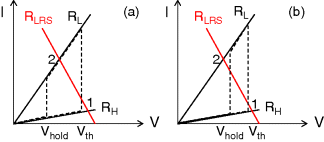
Figure 12.6 (a) Balanced 1S1R structure. (b) Nonfunctional 1S1R structure
Nonlinearity has become an increasingly important select device options, because nonlinear I-V characteristics are relatively easy to implement (e.g., tunneling transport mechanisms). Nonlinear select device parameters can be modulated by different processing conditions. Nonlinearity can also be constructed, for example, using complementary structures. Tradeoffs between ON current and nonlinearity ratio need to be carefully addressed. Since nonlinearity is voltage-dependent, performance of nonlinear select devices also depends on voltage distribution and data patterns in the array. As any other select devices, variability of nonlinear select devices needs to be minimized to control memory parameter distribution in a large array.
Self-selecting capability is attractive for crossbar arrays and may be enabled by self-rectification or intrinsic nonlinearity in memory elements. In either approach, there are often tradeoffs between selector parameters and memory performance. Optimization of the overall memory performance requires comprehensive solutions combining material choices, processing control, and device design. Connecting a memory element to an external select device often requires the middle metal electrode to decouple these two devices, which increases aspect ratio in planar arrays and enlarges the footprint in 3D vertical structure. Self-selecting solutions may help to eliminate this problem.
Most RRAM devices still require a forming process and switching current control. Select devices for RRAM need to provide sufficient current and voltage for forming. It's unlikely that any two-terminal select devices will be able to provide switching control like transistors. External line transistor or serial resistors may provide some current control, but their effectiveness depends strongly on parasitic components in the array. There has been limited research on the switching speed and transient effects of select devices, which could affect the dynamic behavior of memory devices.
Line resistance is neglected in most analysis of select device requirements and crossbar array performance. Line resistance degrades the voltage and current delivered to devices further away from voltage sources in the array, which affect the functionality of both the memory element and select devices. In highly scaled nodes, line resistance may become a critical limiting factor in crossbar array sizes [8]. Contact resistance presents a major challenge for all memory select devices, which becomes increasingly difficult with device scaling.
12.5 Summary
This chapter reviews device options and R&D status of memory select devices targeted for the applications in high-density crossbar arrays and 3D memories. Diodes, volatile switches, and nonlinear devices have been demonstrated as possible solutions for two-terminal select devices. Performance of these potential select devices has been significantly improved recently. Some array-level demonstration has also been reported. Although there are still many challenges to be overcome, it looks promising that some of these extensively explored select device options may provide feasible solutions to enable high-density and low-cost memory and storage technologies in the near future.
References
- 1. International Technology Roadmap of Semiconductors (ITRS) (2011) Emerging Research Devices.
- 2. Crowley, M. et al. (Feb. 2003) 512 Mb PROM with 8 Layers of antifuse/diode cells. ISSCC Tech. Dig. 16.4.
- 3. Kawahara, A. et al. (2013) An 8 Mb multi-layered cross-point ReRAM macro with 443MB/s write throughput. IEEE Journal of Solid-State Circuits, 48(1), 178–185.
- 4. Tanaka, H. et al. (Jun. 2007) Bit Cost Scalable Technology with Punch and Plug Process for Ultra High Density Flash Memory. Symposium VLSI Tech., pp. 14–15.
- 5. Yoon, H.S. et al. (Jun. 2009) Vertical cross-point resistance change memory for ultra-high density non-volatile memory applications. Symposium VLSI Tech., pp. 26–27.
- 6. Flocke, A. and Noll, T.G. (Feb. 2007) Fundamental analysis of resistive nanocrossbars for the use in hybrid Nano/CMOS-memory. Proc. 33rd Eur. Solid-State Circuits Conf., pp. 328–331.
- 7. Flocke, A., Noll, T.G., Kugeler, C. et al. (Aug. 2008) A fundamental analysis of nano-crossbars with non-linear switching materials and its impact on TiO2 as a resistive layer. Proc. 8th IEEE Conf. Nanotech., pp. 319–322.
- 8. Chen, A. (2013) Comprehensive crossbar array model with solutions for line resistance and nonlinear device characteristics. IEEE Transactions on Electron Devices, 60(4), 1316–1326.
- 9. Liang, J., Yeh, S., Wong, S.S., and Wong, H.-S.P. (May 2012) Scaling challenges for the cross-point resistive memory array to sub-10 nm node–an interconnect perspective. Proc. 4th IEEE Intern. Memory Workshop, pp. 1–4.
- 10. Amsinck, C.J., Spigna, N.H.D., Nackashi, D.P., and Franzon, P.D. (2005) Scaling constraints in nanoelectronic random-access memories. Nanotechnology, 16(10), 2251–2260.
- 11. Kim, G.H. et al. (2010) A theoretical model for Schottky diodes for excluding the sneak current in cross bar array resistive memory. Nanotechnology, 21(38), 385202-1–385202-7.
- 12. Ziegler, M.M. and Stan, M.R. (Aug. 2002) Design and analysis of crossbar circuits for molecular nanoelectronics. Proc. 2nd IEEE Conf. Nanotechnol., pp. 323–327.
- 13. Rose, G.S. et al. (Apr.–May 2006) Design approaches for hybrid CMOS/molecular memory based on experimental device data. Proc. 16th ACM Great Lakes Symp. VLSI, pp. 2–7.
- 14. Stan, M.R., Franzon, P.D., Goldstein, S.C. et al. (2003) Molecular electronics: From devices and interconnect to circuits and architecture. Proceedings of the IEEE, 91(11), 1940–1957.
- 15. Zhirnov, V.V., Meade, R., Cavin, R.K., and Sandhu, G. (2011) Scaling limits of resistive memories. Nanotechnology, 22(25), 254027-1-21.
- 16. Yang, B. et al. (2008) Vertical silicon-nanowire formation and gate-all-around MOSFET. IEEE Electron Device Letters, 29(7), 791–793.
- 17. Ghandi, R. et al. (2011) Vertical Si-nanowire n-type tunneling FETs with low subthreshold swing (≤50mV/decade) at Room Temperature. IEEE Electron Device Letters, 32(4), 437–439.
- 18. Wang, C-H. et al. (Dec. 2010) Three-dimensional 4F2 ReRAM cell with CMOS logic compatible process. IEDM Tech. Dig., pp. 664–667.
- 19. Lee, K.J. et al. (Feb. 2007) A 90 nm 1.8 V 512 Mb Diode-Switch PRAM with 266MB/s Read Throughput. ISSCC Tech. Dig., 26.1.
- 20. Liu, T.Y. et al. (Feb. 2013) A 130.7 mm2 2-layer 32 Gb ReRAM memory device in 24 nm technology. ISSCC Tech. Dig., 12.1.
- 21. Oh, J.H. et al. (Dec. 2006) Full integration of highly manufacturable 512 Mb PRAM based on 90 nm technology. IEDM Tech. Dig., pp. 515–518.
- 22. Sasago, Y. et al. (Jun. 2009) Cross-point phase change memory with 4F2 cell size driven by low-contact-resistivity poly-Si diode. Symposium VLSI Tech., pp. 24–25.
- 23. Kinoshita, M. et al. (Jun. 2012) Scalable 3-D vertical chain-cell-type phase-change memory with 4F2 poly-Si diodes. Symposium VLSI Tech., pp. 35–36.
- 24. Lee, S.H. et al. (Dec. 2011) Highly Productive PCRAM Technology Platform and Full Chip Operation: Based on 4F2 (84 nm Pitch) Cell Scheme for 1Gb and Beyond. IEDM Tech. Dig., pp. 47–50.
- 25. Lee, M.J. et al. (2007) A low-temperature-grown oxide diode as a new switch element for high-density, nonvolatile memories. Advanced Materials, 19(1), 73–76.
- 26. Lee, M.J. et al. (Dec. 2007) 2-stack 1D-1R cross-point structure with oxide diodes as switch elements for high density resistance RAM applications. IEDM Tech. Dig., pp. 771–774.
- 27. Lee, M.J. et al. (Dec. 2008) Stack friendly all-oxide 3D RRAM using GaInZnO peripheral TFT realized over glass substrates. IEDM Tech. Dig.
- 28. Ahn, S.E. et al. (2009) Stackable all-oxide-based nonvolatile memory with Al2O3 antifuse and p-CuOx/n-InZnOx diode. IEEE Electron Device Letters, 30(5), 550–552.
- 29. Narushima, S. et al. (2003) A p-type amorphous oxide semiconductor and room temperature fabrication of amorphous oxide p-n heterojunction diodes. Advanced Materials, 15(17), 1409–1413.
- 30. Choi, Y. et al. (2010) High current fast switching n-ZnO/p-Si diode. Journal of Physics D-Applied Physics, 43, 345101-1-4.
- 31. Kim, S., Zhang, Y., McVittie, J.P. et al. (2008) Integrating phase-change memory cell with Ge nanowire diode for crosspoint memory–experimental demonstration and analysis. IEEE Transactions on Electron Devices, 55(9), 2307–2313.
- 32. Shin, Y.C. et al. (2008) (In,Sn)2O3/TiO2/Pt Schottky-type diode switch for the TiO2 resistive switching memory array. Applied Physics Letters, 92(16), 162904–1-3.
- 33. Park, W.Y. et al. (2010) A Pt/TiO2/Ti Schottky-type selection diode for alleviating the sneak current in resistance switching memory arrays. Nanotechnology, 21(19), 195201–1-4.
- 34. Kim, G.H. et al. (2012) Schottky diode with excellent performance for large integration density of crossbar resistive memory. Applied Physics Letters, 100(21), 213508–1-3.
- 35. Huby, N. et al. (2008) New selector based on zinc oxide grown by low temperature atomic layer deposition for vertically stacked non-volatile memory devices. Microelectronic Engineering, 85(12), 2442–2444.
- 36. Huang, J.J., Kuo, C.W., Chang, W.C., and Hou, T.H. (2010) Transition of stable rectification to resistive-switching in Ti/TiO2/Pt oxide diode. Applied Physics Letters, 96(26), 262901-1-3.
- 37. Shima, H. et al. (2008) Control of resistance switching voltages in rectifying Pt/TiOx/Pt trilayer. Applied Physics Letters, 92(4), 043510–1-3.
- 38. Shima, H., Zhong, N., and Akinaga, H. (2009) Switchable rectifier built with Pt/TiOx/Pt trilayer. Applied Physics Letters, 94(8), 082905–1-3.
- 39. Cho, B. et al. (2010) Rewritable switching of one diode–one resistor nonvolatile organic memory devices. Advanced Materials, 22(11), 1228–1232.
- 40. Zuo, Q. et al. (2009) Self-rectifying effect in gold nanocrystal-embedded zirconium oxide resistive memory. Journal of Applied Physiology, 106(7), 073724–1-5.
- 41. Jo, M. et al. (Jun. 2010) Novel Cross-point Resistive Switching Memory with Self-formed Schottky Barrier. Symposium VLSI Tech., pp. 53–54.
- 42. Tran, X.A. et al. (2012) A self-rectifying HfOx-based unipolar RRAM with NiSi electrode. IEEE Electron Device Letters, 33(4), 585–587.
- 43. Tran, X.A. et al. (2013) Self-selection unipolar HfOx-Based RRAM. IEEE Transactions on Electron Devices, 60(1), 391–395.
- 44. Tran, X.A. et al. (2012) A self-rectifying AlOy bipolar RRAM with sub-50-μA set/reset current for cross-bar architecture. IEEE Electron Device Letters, 33(10), 1402–1404.
- 45. Hsu, C.W., Hou, T.H., Chen, M.C. et al. (2013) Bipolar Ni/TiO2/HfO2/Ni RRAM with multilevel states and self-rectifying characteristics. IEEE Electron Device Letters, 34(7), 885–887.
- 46. Lv, H., Li, Y., Liu, Q. et al. (2013) Self-rectifying resistive-switching device with a-Si/WO3 bilayer. IEEE Electron Device Letters, 34(2), 229–231.
- 47. Puthentheradam, S.C., Schroder, D.K., and Kozicki, M.N. (2011) Inherent diode isolation in programmable metallization cell resistive memory elements. Applied Physics A, 102(4), 817–826.
- 48. Kim, K.H., Jo, S.H., Gaba, S., and Lu, W. (2010) Nanoscale resistive memory with intrinsic diode characteristics and long endurance. Applied Physics Letters, 96, 053106-1-3.
- 49. Kau, D. et al. (Dec. 2009) A stackable cross point phase change memory. IEDM Tech. Dig., pp. 617–620.
- 50. Kim, S. et al. (Jun. 2012) Ultrathin (<10 nm) Nb2O5/NbO2 hybrid memory with both memory and selector characteristics for high density 3D vertically stackable RRAM applications. Symposium VLSI Tech., pp. 155–156.
- 51. Lee, J.H. et al. (2012) Threshold switching in Si-As-Te thin film for the selector device of crossbar resistive memory. Applied Physics Letters, 100(12), 123505-1-4.
- 52. Lee, M.J. et al. (Dec. 2012) Highly-Scalable Threshold Switching Select Device based on Chaclogenide Glasses for 3D Nanoscaled Memory Arrays. IEDM Tech. Dig., pp. 33–35.
- 53. Seo, S. et al. (2004) Reproducible resistance switching in polycrystalline NiO films. Applied Physics Letters, 85(23), 5655–5657.
- 54. Lee, M.-J. et al. (2011) A simple device unit consisting of all NiO storage and switch elements for multilevel terabit nonvolatile random access memory. ACS Applied Materials & Interfaces, 3(11), 4475–4479.
- 55. Mott, N.F. (1968) Metal-insulator transition. Reviews of Modern Physics, 40(4), 677–683.
- 56. Lee, M.-J. et al. (2007) Two series oxide resistors applicable to high speed and high density nonvolatile memory. Advanced Materials, 19(22), 3919–3923.
- 57. Son, M. et al. (2011) Excellent selector characteristics of nanoscale VO2 for high-density bipolar ReRAM applications. IEEE Electron Device Letters, 32(11), 1579–1581.
- 58. Son, M. et al. (2012) Self-selective characteristics of nanoscale VOx devices for high-density ReRAM applications. IEEE Electron Device Letters, 33(5), 718–720.
- 59. Ha, S.D., Aydogdu, G.H., and Ramanathan, S. (2011) Metal-insulator transition and electrically driven memristive characteristics of SmNiO3 thin films. Applied Physics Letters, 98(1), 012105-1-3.
- 60. Huang, J.J., Tseng, Y.M., Hsu, C.W., and Hou, T.H. (2011) Bipolar nonlinear Ni/TiO2/Ni selector for 1S1R crossbar array applications. IEEE Electron Device Letters, 32(10), 1427–1429.
- 61. Shin, J. et al. (2011) TiO2-based metal-insulator-metal selection device for bipolar resistive random access memory cross-point application. Journal of Applied Physiology, 109(3), 033712-1-4.
- 62. Lee, W. et al. (Jun. 2012) Varistor-type bidirectional switch (JMAX > 107 A/cm2, selectivity ∼104) for 3D bipolar resistive memory arrays. Symposium VLSI Tech., pp. 37–38.
- 63. Song, Y.H., Park, S.Y., Lee, J.M. et al. (2011) Bidirectional two-terminal switching device for crossbar array architecture. IEEE Electron Device Letters, 32(8), 1023–1025.
- 64. Gopalakrishnan, K. et al. (Jun. 2010) Highly-scalable novel access device based on mixed ionic electronic conduction (MIEC) materials for high density phase change memory (PCM) arrays. Symposium VLSI Tech., 19.4.
- 65. Shenoy, R.S. et al. (Jun. 2011) Endurance and scaling trends of novel access-devices for multi-layer crosspoint memory based on mixed ionic electronic conduction (MIEC) materials. Symposium VLSI Tech., T5B-1.
- 66. Burr, G.W. et al. (Jun. 2012) Large-scale (512 kbit) integration of multilayer-ready access-devices based on mixed-ionic-electronic-conduction (MIEC) at 100% yield. Symposium VLSI Tech., T5.4.
- 67. Virwani, K. et al. (Dec. 2012) Sub-30nm scaling and high-speed operation of fully-confined access-devices for 3D crosspoint memory based on mixed-ionic-electronic-conduction (MIEC) materials. IEDM Tech. Dig., pp. 36–39.
- 68. Linn, E., Rosezin, R., Kuegeler, C., and Waser, R. (2010) Complementary resistive switches for passive nanocrossbar memories. Nature Materials, 9, 403–406.
- 69. Tappertzhofen, S. et al. (2011) Capacity based nondestructive readout for complementary resistive switches. Nanotechnology, 22(39), 395203 1-7.
- 70. Rosezin, R. et al. (2011) Integrated complementary resistive switches for passive high-density nanocrossbar arrays. IEEE Electron Device Letters, 32(2), 191–193.
- 71. Chai, Y. et al. (2011) Nanoscale bipolar and complementary resistive switching memory based on amorphous carbon. IEEE Transactions on Electron Devices, 58(11), 3933–3939.
- 72. Lee, M.J. et al. (2011) A fast, high-endurance and scalable non-volatile memory device made from asymmetric Ta2O5(x/TaO2(x bilayer structures. Nature Materials, 10, 625–630.
- 73. Yang, Y., Sheridan, P., and Lu, W. (2012) Complementary resistive switching in tantalum oxide-based resistive memory devices. Applied Physics Letters, 100(20), 203112-1-4.
- 74. Schmelzer, S., Linn, E., Bottger, U., and Waser, R. (2013) Uniform complementary resistive switching in tantalum oxide using current sweeps. IEEE Electron Device Letters, 34(1), 114–116.
- 75. Bae, Y.C. et al. (2012) Oxygen ion drift-induced complementary resistive switching in homo TiOx/TiOy/TiOx and hetero TiOx/TiON/TiOx triple multilayer frameworks. Advanced Functional Materials, 22(4), 709–716.
- 76. Nardi, F., Balatti, S., Larentis, S., and Ielmini, D. (Dec. 2011) Complementary switching in metal oxides: toward diode-less crossbar RRAMs. IEDM Tech. Dig., pp. 709–712.
- 77. Lee, J. et al. (Dec. 2010) Diode-less nano-scale ZrOx/HfOx RRAM device with excellent switching uniformity and reliability for high-density cross-point memory applications. IEDM Tech. Dig., pp. 452–455.
- 78. Banno, N. et al. (Jun. 2012) Nonvolatile 32 × 32 crossbar atom switch block integrated on a 65-nm CMOS platform. Symposium VLSI Tech., pp. 39–40.
- 79. Liu, X. et al. (2013) Complementary resistive switching in niobium oxide-based resistive memory devices. IEEE Electron Device Letters, 34(2), 235–237.
- 80. Lee, D. et al. (2012) Operation voltage control in complementary resistive switches using heterodevice. IEEE Electron Device Letters, 33(4), 600–602.
- 81. Xie, Y.W., Sun, J.R., Wang, D.J. et al. (2006) Reversible electroresistance at the Ag/La0.67Sr0.33MnO3 interface. Journal of Applied Physiology, 100(3), 033704-1-5.
- 82. Choi, H. et al. (May 2011) The effect of tunnel barrier at resistive switching device for low power memory applications. Proc. 3rd IEEE Intern. Memory Workshop.
- 83. Lee, H.D. et al. (Jun. 2012) Integration of 4F2 selector-less crossbar array 2 Mb ReRAM based on transition metal oxides for high density memory applications. Symposium VLSI Tech., pp. 151–152.
- 84. Chevallier, C.J. et al. (Feb. 2010) A 0.13 μm 64 Mb multi-layered conductive metal-oxide memory. ISSCC Tech. Dig., 14.3.
- 85. Smit, G.D.J., Rogge, S., and Klapwijk, T.M. (2002) Scaling of nano-Schottky-diodes. Applied Physics A, 81(20), 3852–3854.