
10
Macromolecular Memory
Benjamin F. Bory and Stefan C.J. Meskers
Eindhoven University of Technology, The Netherlands
10.1 Chapter Overview
Macromolecular materials, such as polymers, can be used to make electronic memory cells. This chapter focuses on data storage based on resistive switching in diodes incorporating macromolecules. The organization of the chapter is as follows. We start with a brief introduction into the chemical structure and properties of macromolecules. We then sketch the phenomenology of electronic memory effects involving macromolecules and review the current state of the art in polymer memory technology. The subsequent sections are devoted to the electrical and semi-(conducting) properties of polymers and macromolecules and physical–chemical mechanisms of the electronic memory effects. Finally we classify different types of macromolecular memory based on the physical–chemical characteristics of the material involved.
10.2 Macromolecules
10.2.1 Chemical Structure
Macromolecules can be defined as large molecules built up of more than, say, 102 atoms. The class of macromolecules includes synthetic and biological polymers, polyelectrolytes and also encompasses frameworks such as carbon nanotubes and graphene. The backbone of these macromolecules often consists mainly of carbon atoms, sometimes silicon. Two carbon atoms in the chain can be linked via either a single, double or triple bond depending on the number of electron pairs that are shared between the two atoms. Hydrogen and hetero atoms such as oxygen, nitrogen, sulfur can also be incorporated in the chain in various ways and this makes the possible variation in chemical structure almost endless. Compared to other solids, polymers can be characterized as “soft” condensed matter. The solid state structure of a polymer is usually disordered and has considerable internal free volume. The free volume leaves room for motion of the chains in the solid, which in turn allows for migration and diffusion of small molecules and ions and for rearrangements of intermolecular and intramolecular ordering. Furthermore, because of the large size of the molecules, relaxation times to reach thermodynamic equilibrium are often very long. As a consequence, macromolecular materials commonly occur in long-lived, metastable thermodynamic states and might not even reach thermodynamic equilibrium in a time span of years.
10.2.2 Memristive Effects in Macromolecular Materials
The free volume and internal motion allow macromolecules to adapt their structure and conformation in response to external stimuli and perturbations. This also extends to the electrical properties of macromolecules. In the past decade it has been shown that using a macromolecular material as insulator in a Metal–Insulator–Metal (MIM) structure, one can realize diodes whose electrical resistance can be modified by application of electrical bias voltage. Table 10.1 gives an overview of review articles that describe progress and achievements in this field.
Table 10.1 Reviews on diodes incorporating organic materials showing electronic memory effects in their electrical resistivity
| Title of review | Reference details | Description |
| Electrical switching and bistability in organic/polymeric thin films and memory devices [1] | Adv. Funct. Mater. vol. 16, pp. 1001–1014, 2006. | Resistive switching in π-conjugated polymers |
| Nonvolatile memory elements based on organic materials [2] | Adv. Mater. vol. 19, pp. 1452–1463, 2007. | Classification of electrical characteristics and minimal performance specifications |
| Nanoionics-based resistive switching memories [3] | Nat. Mater. vol. 6, pp. 833–840, 2007. | Redox process involving metal ions; growth/dissolution of filaments |
| Polymer electronic memories: materials, devices and mechanisms [4] | Prog. Polym. Sci. vol. 33, pp. 917–978, 2008. | Mechanism in relation to chemical structure of polymers |
| Polymer and organic nonvolatile memory devices [5] | Chem. Mater. vol. 23, pp. 341–358, 2011. | Principles of operation and feasibility |
| Recent results on organic-based molecular memories [6] | Curr. Appl. Phys. vol. 11, pp. e49–e57, 2011. | Molecular aspects of organic memory |
| Progress in nonvolatile memory devices based on nanostructured materials and nanofabrication [7] | J. Mater. Chem. vol. 21, pp. 14 907–14 112, 2011. | Fabrication and integration of organic memory and device architecture |
| Donor–acceptor polymers for advanced memory device applications [8] | Polym. Chem. vol 2, pp. 2169–2174, 2011. | Polyimide polymers |
| Organic resistive memory devices: performance enhancement, integration, and advanced architectures [9] | Adv. Funct. Mater. vol 21, pp. 2806–2829, 2011. | Architecture, operation and integration of polymer memory; inventory of the different mechanisms and the integration into electronics |
| Organic resistive nonvolatile memory materials [10] | MRS Bull. vol. 37, pp. 144–149, 2012. | Performance and requirements; integrated circuit architectures |
| Advanced polyimide materials: syntheses, physical properties and applications [11] | Prog. Polym. Sci. vol. 37, pp. 907–974, 2012. | Synthesis and properties of polyimide materials; functionalized polyimids for resistive memory |
| Polyimide memory: a pithy guideline for future applications [12] | Polym. Chem. vol. 4, pp. 16–30, 2013. | Classification of memory effects in polyimides; electronic structures of polyimide materials in relation to memory |
The change in resistance may be transient and disappear when short-circuiting the diode (volatile memory) or could be semi-permanent under short-circuit conditions (nonvolatile memory). For the latter memristive devices, one can differentiate between write once read many (WORM, W) and rewriteable memory cells. The rewriteable cells can be further subdivided into cells that require write and erase voltages of opposite polarity (Bipolar, B) and cells that can be operated using write and erase voltages of the same polarity (Unipolar, U).
Attractive features of macromolecular memory include the possibility to use solution-based deposition methods such as printing and casting of the active layers. In addition, flexible, lightweight, and disposable substrates may be used. Furthermore because macromolecular memory is essentially a thin film technology and one can make economic use of raw materials (Figure 10.1).
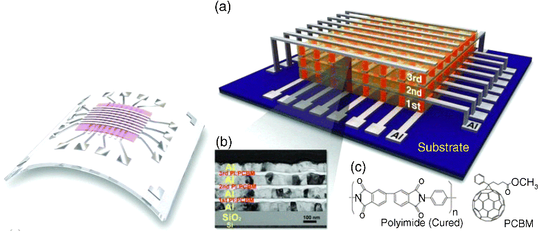
Figure 10.1 Macromolecular memory: flexible substrates (left, [60]) and 3-D integration (right, a–c, [26]. Copyright: Wiley VCH
10.2.3 Current State of Macromolecular Memory
In the last decade enormous progress has been made in the realization of macromolecular memory. Resistive switching has been shown to occur locally and downscaling to nm lengths is feasible. Projected retention times on the order of 10 years have been realized and switching is possible using short voltage pulses (submicrosecond). Integration into arrays has been demonstrated. So far, a complete device technology seems not to have been disclosed. A main challenge for macromolecular memory is still to understand and control the resistive switching. As will become clear, macromolecular memory operates close to the threshold for electrical breakdown. Reproducibility of the switching characteristics is often an issue. In view of the very stringent requirements regarding uniformity, cycle endurance, and bit error rate for application as NAND flash, variability in the characteristic of cells may be an issue.
10.3 Elementary Physical Chemistry of Macromolecular Memory
10.3.1 Required Activation Barrier between Stable States
For a rewriteable, nonvolatile memory, one would like to have a molecular system that is bistable, having two distinct stable states (“ON” and “OFF”) separated by a barrier in energy (see Figure 10.2). For electronic memory applications, the ON and OFF states should differ in charge transport related properties, namely delocalization length of charge carriers and energies of the electron and holes states on the polymer. The transition between the ON and OFF states is in essence a monomolecular chemical reaction. The transition state theory developed by Eyring describes the rate of chemical reactions and allows one to estimate the rate of interconversion between ON and OFF state, kON/OFF in s−1, as a function of the height of the energy barrier separating the two minima [13]. To warrant a lifetime of at least 10 years for the ON and OFF state, the barrier in between the two states should have a height of at least 1.25 eV of Gibbs free energy.
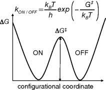
Figure 10.2 Gibbs Free energy ΔG as function of a generalized configurational coordinate for a bistable molecule. The rate of spontaneous interconversion between ON and OFF states, kON/OFF, is determined by the height of the barrier (ΔG‡) in between the two stable states and temperature. For a lifetime of ON and OFF states of 10 years at room temperature, a minimal barrier height of ΔG‡ = 1.25 eV is required according to molecular transition state theory
The barrier should have sufficient width to suppress quantum mechanical tunneling between the states. Application of a potential difference over the memory cell should lead to rapid conversion between the ON and OFF states. From the estimated barrier height it then follows that the minimal voltages needed to switch the cell will exceed 1.25 V.
Furthermore, memory cells relying on trapping of charges can most likely not be realized with semiconducting materials with a bandgap smaller than 1.25 eV.
One might argue that small molecules are inherently less stable and more prone to thermodynamical and quantum mechanical fluctuations than bulk phases in large crystals. So is there any experimental evidence for small bistable molecular systems with lifetime of the individual states exceeding 10 years? Amino acids are small molecules with fewer than 12 carbon atoms, that serve as monomeric units of proteins and polypeptides. Amino acids can exist in two mirror image related stable configurations labeled L and D. Even though the two forms have identical energies, in living plants and animals only the L form is produced and biochemically active. Analysis of fossils has shown that interconversion of the L into the D forms takes place on a time scale of 103 years [14]. This shows that bistable molecular systems with interconversion sufficiently slow for electronic memory applications indeed exist.
10.3.2 Electronic Structure of Macromolecules: Insulators, Semiconductors, Conductors
Depending on the type of connection between the carbon atoms, macromolecules behave electrically as either insulators, semiconductors or conductors. The origin of the diversity lies in the different possible types of coordination of substituents around the carbon atom. Two neighboring carbon atoms can form a chemical bond by sharing two valence electrons between them, with each atom donating one electron. The two electrons forming the bond must have antiparallel spin. Because carbon has four valence electrons it can bind to maximally four other atoms. Electrostatic repulsion between the electron pairs forming the bonds is minimized when the four carbon atoms binding to the central one are arranged in the form of a tetrahedron. Hybridization of the hydrogen like 2s and three 2p orbitals around the carbon nucleus into four equivalent sp3 orbitals facilitates the formation of these four bonds. The resulting atomic arrangement is that of diamond, a material that can be characterized as a wide (5.4 eV) indirect bandgap semiconductor.
Within the diamond lattice, electrons and holes have high and almost equal mobility (2 × 103 cm2/Vs).
In another allotrope of carbon, graphite, each carbon atom is bound to only three neighboring atoms and one valence electron per atom is delocalized over the honeycomb hexagonal sheet of carbon atoms. In this case, repulsion between electron pairs forming the bonds results in a planar triangular arrangement of the three substituents. Hybridization of the carbon 2s with two 2p orbitals to sp2 orbitals can facilitate this bonding. This leaves one 2p orbital unhybridized containing one electron. Overlap between unhybridized 2p orbitals on neighboring sp2 hybridized carbon atoms allows for quantum mechanical delocalization of these electrons and gives rise to (semi-)conducting properties of the molecular material. The delocalization of the electrons in the 2p atomic orbitals contributes to the bonding between two neighboring carbon atoms (now sharing a double bond) and the two atoms are said to be π-conjugated. A single layer of graphite, graphene, contains delocalized electrons and may be classified as a zero bandgap semiconductor. Electron and hole mobilities are exceptionally high (estimated > 2 × 104 cm2/Vs [15]) and relate, from a chemical point of view, to the stability of the two-dimensional hexagonal lattice against distortion.
Replacing two of the coordinating carbon atoms by hydrogen, a polymeric structure may be obtained (polyacetylene, see Figure 10.3). In this macromolecule, or π-conjugated polymer (named after the double or π-bond) one electron per carbon atom is still delocalized. Due to pairing of neighboring carbon atoms in the chain (Peierls distortion), a band gap opens (1.5 eV) and the resulting chain is alternating longer, singly bonded carbon atom pairs and shorter doubly bonded pairs. Because of the presence of double or π-bonds, polyacetylene is a π-conjugated polymer. The mobilities of charge carriers along the chain are reduced because of polaron formation and bulk mobilities are severely limited by poor intermolecular transport of carriers and trapping on impurities and defects. Carrier mobilities in purified molecular materials rarely exceed 1 cm2/Vs and for π-conjugated polymers usually fall in the range 10−3–10−7 cm2/Vs. π-Conjugated polymers can be made conductive by oxidative or reductive doping. In the case of polyacetylene, doping with molecular iodine (I2) results in a hole conducting material with conductivity approaching that of metals. By introducing dopants which themselves are macromolecules, diffusion, sublimation, and electromigration of the dopants can be suppressed and stable molecular conductors can be obtained. A well known example is poly(3,4-ethylenedioxythiophene): poly(styrenesulfonate), or PEDOT:PSS, where positive charge carriers on the π-conjugated EDOT polymer are stabilized by the deprotonated and negatively charged polystyrene sulfonate polymer (PSS).
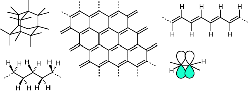
Figure 10.3 Left: Diamond lattice and polyethene with sp3 hybridized carbon atoms and saturated bonds. Middle: Graphene sheet. Right: Polyacetylene polymer with two overlapping atomic 2pz orbitals on two neighboring sp2 hybridized carbon atoms forming a double bond
10.3.3 Inducing Changes by Application of Bias Voltage: Electrochemistry
As mentioned above, bias voltages ≥1.25 V will be needed for switching between bistable states of macromolecular memory. Currently in NAND flash technology, voltages up to 20 V are used to program the floating gate transistor. The question arises: which chemical changes might one expect to be induced by applying voltages in the range 1–101 volt? From physical chemistry, the energies needed to break a chemical bond are well known. For a carbon–carbon single bond, 3.6 eV is required to break the bond. To split the strongest homodimeric bond known in organic chemistry, the nitrogen–nitrogen triple bond N![]() N, 9.8 eV is required. Taking into account that macromolecular memory is a thin film technology and that the bias voltage applied often results in a potential drop localized over only a narrow spatial region in the organic materials, programming voltages up to 10 V could well lead to charge carriers with up to 10 eV of kinetic energy. In principle, the 10 eV energy of the electron suffices to break any chemical bond in a molecule. We remark that, in electrochemistry, energies needed for a chemical reaction can be measured quantitatively, using polar solvents and adding salt ions (electrolyte) to localize the electric field strength in a small region close to an electrode. From electrochemistry, it is well known that within a voltage range up to a few volts, almost any chemical conversion can be driven, including oxidation and reduction of all metals. This simple line of argument illustrates the tremendous difficulties that one may face when trying to unravel mechanistic aspects of memristive effects in organic molecular materials: with programming voltages typically in the range 2–8 V a multitude of chemical processes is likely to be induced.
N, 9.8 eV is required. Taking into account that macromolecular memory is a thin film technology and that the bias voltage applied often results in a potential drop localized over only a narrow spatial region in the organic materials, programming voltages up to 10 V could well lead to charge carriers with up to 10 eV of kinetic energy. In principle, the 10 eV energy of the electron suffices to break any chemical bond in a molecule. We remark that, in electrochemistry, energies needed for a chemical reaction can be measured quantitatively, using polar solvents and adding salt ions (electrolyte) to localize the electric field strength in a small region close to an electrode. From electrochemistry, it is well known that within a voltage range up to a few volts, almost any chemical conversion can be driven, including oxidation and reduction of all metals. This simple line of argument illustrates the tremendous difficulties that one may face when trying to unravel mechanistic aspects of memristive effects in organic molecular materials: with programming voltages typically in the range 2–8 V a multitude of chemical processes is likely to be induced.
10.3.4 Filamentation
As mentioned above, by applying potential differences on the order of 10 V over a thin organic layer, one can drive a molecular material very far out of thermodynamic equilibrium. Note that the low mobility of charge carriers contributes to localizing the electric field strength to narrow regions. In soft condensed matter, the behavior of molecular systems far away from equilibrium has been studied in considerable detail in the last half century. One of the striking outcomes is that when a system is driven far out of equilibrium, spontaneous self-organization into patterns and structures is possible. In contrast, under near equilibrium conditions, such self-organization processes would not be favorable because of the reduction of entropy associated with the emergence of organization, patterns and structures [16]. One of the self-organization processes studied in detail is filamentation, which occurs for instance in the transmission of light when the strength of the optical electric field becomes so high that the refractive index of the material changes. The light can then focus itself into small filaments [17]. Other examples of filamentation are the formation of plasma arcs [18]. Filamentation of electrical current in planar organic memory diodes is often observed and should most likely be considered as an integral part of the response of the materials to the large thermodynamic driving force applied.
10.4 Classes of Macromolecular Memory Materials and Their Performance
In this section we give an overview of recent reports on macromolecular memory (see Table 10.2). Because the mechanism of switching is often unclear we classify the memory diodes according to the type of macromolecular material used.
Table 10.2 Memory performance characteristics for macromolecular memory
| Material | MIM architecture | Type | Von | Voff | On/Off | Retention (s) | Endurance |
| PEO-AgClO4 [19] | Pt//Ag | B | 1 | −1 | 105 | 105 | 10 |
| π-Conjugated polyelectolyte [20] | Ag//p+-Si | B | 3 | −2 | 104 | 105 | nd |
| Donor–acceptor polyimide [21] | ITO//Al | B | 2.7 | −1.5 | 104 | 104 | nd |
| Donor–acceptor polyimide | ITO//Al | U | 2.2 | 1 | 104 | 104 | nd |
| Donor–acceptor polyimide | ITO//Al | W | 2 | ||||
| PEDOT:PSS [22] | Al//Al | B | −2.5 | 1.2 | 105 | 105 | 10 |
| PEDOT:PSS [23] | Au//Au | U | 4 | 1 | 102 | 104 | nd |
| PEDOT:PSS [24] | Al//Cu | B | 1 | −0.8 | 104 | 104 | nd |
| Fullerene [25] | ITO//Al | U | 4 | 2 | 105 | 104 | 101 |
| Fullerene [26] | Al//Al | U | 5 | 10 | 103 | 107 | 102 |
| Carbon nanotube [27] | Al//Al | B | −2 | 2 | 102 | 105 | 102 |
| Diamond-like carbon [28] | W//Pt | U | 1.2 | 0.4 | 300 | 103 | 103 |
| Diamond-like carbon [29] | Ti//Pt | U | 1.4 | −1.5 | 10 | 104 | nd |
| Amorphous Carbon [30] | Ag//Ag | B | 6 | −7 | 30 | 106 | 30 |
| Graphite [31] | U | 3 | 6 | 106 | 106 | 106 | |
| Graphene [32] | ITO/PMMA//PMMA/Al | B | 3.5 | −4 | 106 | 105 | 105 |
| B: bipolar; U: unipolar; W: WORM; nd: not determined. | |||||||
10.4.1 Saturated Macromolecules
Polymers that do not contain any double bonds are insulators and charge carrier injection via a metal contact into these materials is practically impossible. However these polymers may still be used as host materials in memory applications, when combined with additives that can take care of carrier transport. For instance, polyethylene oxide (PEO) is a polymer that can solvate ions. PEO combined with the silver salt AgClO4 can be used to realize memory cells. In AgClO4-PEO cells, electrochemical conversion of silver ions into metallic silver gives rise to the formation and dissolution of metal filaments, leading to resistive switching [19]. A disadvantage of these electrochemical cells is that the amount of charge needed to switch the diode depends on the history of the diode. The amount of current needed to switch the diode is only minimal close to the percolation threshold via the metallic filament. Some saturated polymers containing fluor substituents are ferroelectric and can be used to make a capacitive memory. When blended with semiconducting polymer resistive switching diodes have been accomplished [33]. For further information, we refer the reader to the discussion of ferroelectric memories in Chapters 6 and 9.
10.4.2 Macromolecules with π-Conjugation
10.4.2.1 Dynamic Doping
Organic molecules containing double bonds (π-conjugation) usually have semiconducting properties. The presence of charged dopants in these materials can change barriers for charge injection and the charge carrier density. Migration of charged dopants under the influence of applied bias leads to memristive effects [34]. The memory functionality of the macromolecular material can be enhanced further by doping with metal ions that can also be reduced electrochemically to metal filaments.
10.4.2.2 Donor–Acceptor Polymers
A large research effort has focused on polyimide polymers functionalized with π-conjugated moieties that have pronounced electron donating and electron accepting properties [8,11,12]. These materials often show volatile resistive switching, but nonvolatile behavior has also been observed, including both WORM and rewritable characteristics. The volatile behavior has been related to the presence of an ionized electronic state of the donor acceptor polymer (charge transfer state) in which the electron donating unit has transferred an electron to the electron accepting moieties.
10.4.2.3 Conducting Polymers
Conducting polymers such as PEDOT:PSS have been used as WORM, relying on destructive processes induced at high current densities [35,36]. However also rewritable memory cells have been realized with PEDOT:PSS and a number of studies indicate the importance of the interface between polymer and metal contact in the switching and indicate an active role of native oxides [37–39].
10.4.2.4 Carbon Allotropes
Fullerenes are spheroidal π-conjugated molecules that in comparison with π-conjugated polymers show high electron and hole mobilities. When mixed with a host polymer, a solution processable material is obtained that shows rewriteable memory effects after optimization of the mixing ratio characteristic [40–42]. Very promising memory characteristics have been reported and integration of cells into 2-D [43,44] and 3-D [26] has been achieved. A number of studies have indicated the importance of an interfacial oxide layer in the resistive switching process [26,43–46]. Carbon nanotubes can also be applied in memories and also here indications for the involvement of an interfacial oxide layer in the switching have been obtained (Al2O3 [27,47], SiO2 [48]). Graphene can give rise to bipolar switching [49] and sometimes WORM [50] memory effects. Graphene oxide functionalized with polymer chains gives a solution processable macromolecular material, displaying memory effects in combination with ITO and Al electrodes [51–53]. Finally, amorphous carbon and diamond-like carbon are amorphous carbon allotropes that show electronic memory effects in MIM devices. Amorphous carbon contains both sp3 and sp2 hybridized carbon atoms. Variation in the ratio and distribution of the semi-conducting (sp2) and insulating (sp3) varieties induced by the application of electrical stress has been suggested to lead to memory effects [54,55].
10.4.2.5 Hybrid Diodes Involving a Dedicated Inorganic Switching Layer
A number of studies have been devoted to MIM structures incorporating a (macro-)molecular layer in combination with a dedicated inorganic switching layer consisting of metal oxide [56,57] or metal halide [58]. Similar to metal oxide memory cells, these hybrid devices require an electroforming step before resistive memory effects become apparent. The electroforming process is induced by bias voltage stress and can be subdivided into different stages. The early stages involve charge trapping at the interface between the macromolecular semiconductor and the metal oxide [59]. The final step of electroforming involves soft breakdown of the inorganic insulator and is related to hole injection [58].
10.5 Perspectives
Memory cells using macromolecular materials that rely on resistive switching show excellent memory characteristics when operated as isolated cells under single write/read/erase events. Large-scale integration does not seem to have been realized, and therefore performance as integrated memory is currently difficult to estimate. The occurrence of a so-called dead time in repeated switching could be a major hurdle. Key opportunities of macromolecular memory include the low cost of raw materials and deposition methods, for example, printing and coating. Furthermore, memory cells incorporating environmentally friendly materials can be realized. This provides applications in low-end, disposable electronics on, for example, flexible substrates such as paper or plastic.
| Summary of macromolecular memory parameters: | ||
| Cell size | Demonstrated | 130 nm |
| Projected | 10 nm | |
| Density | Demonstrated | Not known |
| Projected | Comparable to ferroelectric and phase change | |
| Device speed (switching speed for logic devices; reading/writing speed for memory devices | Demonstrated | 15 ns |
| Projected | <10 ns | |
| Circuit speed | Demonstrated | Not known |
| Projected | Depends on “dead-time” | |
| Operation voltages | Demonstrated | <6 V |
| Projected | Not known | |
| Switching energy | Demonstrated | 5E-11 Joule/bit |
| Projected | Not known | |
| Endurance | Demonstrated | >1E5 |
| Projected | Not known | |
| Retention (for memory) | Demonstrated | ∼1 yr |
| Projected | ||
| Binary throughput | Demonstrated | Not known |
| Projected | Not known |
10.6 Summary
Macromolecular materials can give rise to a wide variety of electronic memory effects. Although impressive memory characteristics have been obtained, lack of understanding and control over the switching mechanisms is still a major issue.
Acknowledgments
The work of BBF forms part of research programme of the Dutch Polymer Institute (DPI 704). We thank D.M. De Leeuw and H.L. Gomes for stimulating discussion.
References
- 1. Yang, Y., Ouyang, J., Ma, L.P. et al. (2006) Electrical switching and bistability in organic/polymeric thin films and memory devices. Advanced Functional Materials, 16(8), 1001–1014.
- 2. Scott, J.C. and Bozano, L.D. (2007) Nonvolatile memory elements based on organic materials. Advanced Materials, 19(11), 1452–1463.
- 3. Waser, R. and Aono, M. (2007) Nanoionics-based resistive switching memories. Nature Materials, 6(11), 833–840.
- 4. Ling, Q.-D., Liaw, D.-J., Zhu, C. et al. (2008) Polymer electronic memories: materials, devices and mechanisms. Progress in Polymer Science, 33(10), 917–978.
- 5. Heremans, P., Gelinck, G.H., Muller, R. et al. (2011) Polymer and organic nonvolatile memory devices. Chemistry of Materials, 23(3), 341–358.
- 6. Salvo, B.De., Buckley, J., and Vuillaume, D. (2011) Recent results on organic-based molecular memories. Current Applied Physics, 11(2), E49–E57.
- 7. Lee, J.-S. (2011) Progress in non-volatile memory devices based on nanostructured materials and nanofabrication. Journal of Materials Chemistry, 21(37), 14097–14112.
- 8. Liu, C.-L. and Chen, W.-C. (2011) Donor–acceptor polymers for advanced memory device applications. Polymer Chemistry, 2(10), 2169–2174.
- 9. Cho, B., Song, S., Ji, Y. et al. (2011) Organic resistive memory devices: Performance enhancement, integration, and advanced architectures. Advanced Functional Materials, 21(15), 2806–2829.
- 10. Lee, T. and Chen, Y. (2012) Organic resistive nonvolatile memory materials. MRS Bulletin, 37(2), 144–149.
- 11. Liaw, D.-J., Wang, K.-L., Huang, Y.-C. et al. (2012) Advanced polyimide materials: syntheses, physical properties and applications. Progress in Polymer Science, 37(7), 907–974.
- 12. Kurosawa, T., Higashihara, T., and Ueda, M. (2013) Polyimide memory: a pithy guideline for future applications. Polymer Chemistry, 4(1), 16–30.
- 13. Atkins, P.W. and Depaula, J. (2009) Physical Chemistry, Oxford University Press, Oxford.
- 14. Poinar, H.N., Höss, M., Bada, J.L., and Pääbo, S. (1996) Amino acid racemization and the preservation of ancient DNA. Science, 272(5263), 864–866.
- 15. Geim, A.K. and Novoselov, K.S. (2007) The rise of graphene. Nature Materials, 6(3), 183–191.
- 16. Cross, M.C. and Hohenberg, P.C. (1993) Pattern formation outside of equilibrium. Reviews of Modern Physics, 65(3), 851–1112.
- 17. Couairon, A. and Mysyrowicz, A. (2007) Femtosecond filamentation in transparent media. Physics Reports-Review Section of Physics Letters, 441(2–4), 47–189.
- 18. Purwins, H.-G. and Berkemeier, J. (2011) Self-organized patterns in planar low-temperature DC gas discharge. IEEE Transactions on Plasma Sciences, 39(11), 2116–2117.
- 19. Wu, S., Tsuruoka, T., Terabe, K. et al. (2011) A polymer-electrolyte-based atomic switch. Advanced Functional Materials, 21(1), 93–99.
- 20. Cho, B., Yun, J.M., Song, S. et al. (2011) Direct observation of Ag filamentary paths in organic resistive memory devices. Advanced Functional Materials, 21(20), 3976–3981.
- 21. Li, Y., Fang, R., Ding, S., and Shen, Y. (2011) Rewritable and non-volatile memory effects based on polyimides containing pendant carbazole and triphenylamine groups. Macromolecular Chemistry and Physics, 212(21), 2360–2370.
- 22. Yang, J., Zeng, F., Wang, Z.S. et al. (2011) Modulating resistive switching by diluted additive of Poly(vinylpyrrolidone) in Poly(3,4-ethylenedioxythiophene):Poly(styrenesulfonate). Journal of Applied Physics, 110(11), 114518.
- 23. Liu, X., Ji, Z., Tu, D. et al. (2009) Organic nonpolar nonvolatile resistive switching in Poly(3,4-ethylene-dioxythiophene): Polystyrenesulfonate thin film. Organic Electronics, 10(6), 1191–1194.
- 24. Wang, Z., Zeng, F., Yang, J. et al. (2012) Resistive switching induced by metallic filaments formation through Poly(3,4-ethylene-dioxythiophene): Poly(styrenesulfonate). ACS Applied Materials & Interfaces, 4(1), 447–453.
- 25. Hahm, S.G., Kang, N.-G., Kwon, W. et al. (2012) Programmable bipolar and unipolar nonvolatile memory devices based on Poly(2-(N-carbazolyl)ethyl methacrylate) end-capped with fullerene. Advanced Materials, 24(8), 1062–1066.
- 26. Song, S., Cho, B., Kim, T.-W. et al. (2010) Three-dimensional integration of organic resistive memory devices. Advanced Materials, 22(44), 5048–5053.
- 27. Hwang, S.K., Lee, J.M., Kim, S. et al. (2012) Flexible multilevel resistive memory with controlled charge trap B- and N-Doped Carbon Nanotubes. Nano Letters, 12(5), 2217–2221.
- 28. Fu, D., Xie, D., Feng, T. et al. (2011) Unipolar resistive switching properties of diamondlike carbon-based RRAM devices. IEEE Electron Device Letters, 32(6), 803–805.
- 29. Peng, P., Xie, D., Yang, Y. et al. (2012) Resistive switching behavior in diamond-like carbon films grown by pulsed laser deposition for resistance switching random access memory application. Journal of Applied Physics, 111(8), 084501.
- 30. Chai, Y., Wu, Y., Takei, K. et al. (2011) Nanoscale bipolar and complementary resistive switching memory based on amorphous carbon. IEEE Transactions on Electron Devices, 58(11), 3933–3939.
- 31. Li, Y., Sinitskii, A., and Tour, J.M. (2008) Electronic two-terminal bistable graphitic memories. Nature Materials, 7(12), 966–971.
- 32. Son, D.I., Kim, T.W., Shim, J.H. et al. (2010) Flexible organic bistable devices based on graphene embedded in an insulating Poly(methyl methacrylate) polymer layer. Nano Letters, 10(7), 2441–2447.
- 33. Asadi, K., De Leeuw, D.M., De Boer, B., and Blom, P.W.M. (2008) Organic Non-volatile memories from ferroelectric phase-separated blends. Nature Materials, 7(7), 547–550.
- 34. Sim, R., Chan, M.Y., Wong, A.S.W., and Lee, P.S. (2011) Alternative resistive switching mechanism based on migration of charged counter-ions within conductive polymers. Organic Electronics, 12(1), 185–189.
- 35. D. M., DeLeeuw., Geuns, T.C.T., and De Brito, B.C. (2011) “Switching element used as memory element e.g. write-once-read-many memory element” WO patent WO2008087566-A1.
- 36. Wang, J., Cheng, X., Caironi, M. et al. (2011) Entirely solution-processed write-once-read-many-times memory devices and their operation mechanism. Organic Electronics, 12(7), 1271–1274.
- 37. Kim, J.Y., Jeong, H.Y., Kim, J.W. et al. (2011) Critical role of top interface layer on the bipolar resistive switching of Al/PEDOT:PSS/Al Memory Device. Current Applied Physics, 11(2), e35–e39
- 38. Ha, H. and Kim, O. (2010) Electrode-material-dependent switching characteristics of organic nonvolatile memory devices based on Poly(3,4-ethylene dioxythiophene): poly(styrenesulfonate) Film. IEEE Electron Device Letters, 31(4), 368–370.
- 39. Jeong, H.Y., Kim, J.Y., Yoon, T.H., and Choi, S.-Y. (2010) Bipolar resistive switching characteristics of Poly(3,4-ethylene-dioxythiophene): Poly(styrenesulfonate) thin film. Current Applied Physics, 10(1), e46–e49
- 40. Chen, J.-C., Liu, C.-L., Sun, Y.-S. et al. (2012) Tunable electrical memory characteristics by the morphology of self-assembled block copolymers: PCBM nanocomposite films. Soft Matter, 8(2), 526–535.
- 41. Lian, S.-L., Liu, C.-L., and Chen, W.-C. (2011) Conjugated fluorene based rod-coil block copolymers and their PCBM composites for resistive memory switching devices. ACS Applied Materials & Interfaces, 3(11), 4504–4511.
- 42. Hsu, J.-C., Liu, C.-L., Chen, W.-C. et al. (2011) A Supramolecular approach on using Poly(fluorenylstyrene)-block-poly(2-vinylpyridine):PCBM composite thin films for non-volatile memory device applications. Macromolecular Rapid Communications, 32(6), 528–533.
- 43. Kim, J.J., Cho, B., Kim, K.S. et al. (2011) Electrical characterization of unipolar organic resistive memory devices scaled down by a direct metal-transfer method. Advanced Materials, 23(18), 2104–2108.
- 44. Cho, B., Song, S., Ji, Y., and Lee, T. (2010) Electrical characterization of organic resistive memory with interfacial oxide layers formed by O2 plasma treatment. Applied Physics Letters, 97(6), 063305.
- 45. Ko, S.H., Yoo, C.H., and Kim, T.W. (2012) Electrical bistabilities and memory stabilities of organic bistable devices utilizing C60 molecules embedded in a polymethyl methacylate matrix with an Al2O3 blocking layer. Journal of the Electrochemical Society, 159(8), G93–G96.
- 46. Siebeneicher, P., Kleemann, H., Leo, K., and Lüssem, B. (2012) Non-volatile organic memory devices comprising SiO2 and C60 showing 104 switching cycles. Applied Physics Letters, 100(19), 193301.
- 47. Ávila-Niño, J.A., Machado, W.S., Sustaita, A.O. et al. (2012) Organic low voltage rewritable memory device based on PEDOT:PSS/f-MWCNTs Thin Film. Organic Electronics, 13(11), 2582–2588.
- 48. Yao, J., Jin, Z., Zhong, L. et al. (2009) Two-terminal nonvolatile memories based on single-walled carbon nanotubes. ACS Nano, 3(12), 4122–4126.
- 49. Wu, C., Li, F., Zhang, Y. et al. (2011) Highly reproducible memory effect of organic multilevel resistive-switch device utilizing graphene oxide sheets/polyimide hybrid nanocomposite. Applied Physics Letters, 99(4), 042108.
- 50. Ji, Y., Choe, M., Cho, B. et al. (2012) Organic nonvolatile memory devices with charge trapping multilayer graphene film. Nanotechnology, 23(10), 105202.
- 51. Liu, G., Zhuang, X., Chen, Y. et al. (2009) Bistable electrical switching and electronic memory effect in a solution-processable graphene oxide-donor polymer complex. Applied Physics Letters, 95(25), 253301.
- 52. Zhang, B., Liu, Y.-L., Chen, Y. et al. (2011) Nonvolatile rewritable memory effects in graphene oxide functionalized by conjugated polymer containing fluorene and carbazole units. Chemistry - A European Journal, 17(37), 10304–10311.
- 53. Yu, A.-D., Liu, C.-L., and Chen, W.-C. (2012) Supramolecular block copolymers: graphene oxide composites for memory device applications. Chemical Communications, 48, 383–385.
- 54. Ufert, K. (2011) “Memory element using reversible switching between SP2 and SP3 hybridized carbon” US patent US8030637-B2.
- 55. Sebastian, A., Pauza, A., Rossel, C. et al. (2011) Resistance switching at the nanometre scale in amorphous carbon. New Journal of Physics, 13, 013020.
- 56. Muller, Ch., Deleruyelle, D., Müller, R. et al. (2011) Resistance change in memory structures integrating CuTCNQ nanowires grown on dedicated HfO2 switching layer. Solid-State Electronics, 56, 168–174.
- 57. Verbakel, F., Meskers, S.C.J., Janssen, R.A.J. et al. (2007) Reproducible resistive switching in nonvolatile organic memories. Applied Physics Letters, 91(19), 192103.
- 58. Bory, B.F., Gomes, H.L., Janssen, R.A.J. et al. (2012) Role of hole injection in electroforming of lif-polymer memory diodes. Physical Chemistry C, 116(23), 12443–12447.
- 59. Chen, Q., Bory, B.F., Kiazadeh, A. et al. (2011) Opto-electronic characterization of electron traps upon forming polymer oxide memory diodes. Applied Physics Letters, 99(8), 083305.
- 60. Li, T., Hu, W., and Zhu, D. (2010) A review of experimental testbeds of molecular electronic devices. Advanced Materials, 22, 286.