
9
Electronic Effect Resistive Switching Memories
An Chen
GLOBALFOUNDRIES Inc., USA
9.1 Introduction
Mainstream memory technologies, including SRAM, DRAM, and Flash memories, are all CMOS-based and face scaling challenges. Recently, many novel memory device concepts have emerged as candidates for the next-generation nonvolatile memory technologies, including phase change memory (PCM), spin transfer torque RAM (STT-RAM), resistive RAM (RRAM), and so on. Although many emerging memories store information in switchable resistance levels, the name RRAM usually refers to the two-terminal metal–insulator–metal (MIM) resistive switching devices based on metal oxides. These devices can be electrically switched between a high resistance state (HRS, or off-state) and a low resistance state (LRS, or on-state). Multi-level cell (MLC) can be achieved with appropriate switching control (e.g., current compliance, switching voltage, etc.) or material stack engineering (e.g., multi-layer oxides). The HRS-to-LRS switching is known as “set” (or “program”) and the LRS-to-HRS switching as “reset” (or “erase”). The set and reset switching may occur in the same voltage polarity direction (“unipolar switching”) or in the opposite directions (“bipolar switching”).
Resistive switching in metal oxides is not a new phenomenon [1–3]. Hysteretic current-voltage (I-V) characteristics or negative differential resistance (NDR) was reported on numerous metal oxides, for example, TiOx [4,5], NiOx [6], AlOx [7], NbOx [8], and so on. Some switching models were also proposed to explain these phenomena. One of them is based on the charge trapping that modifies band structure and transport properties, that is, Simmons-Verderber model [9]. Another model is based on the formation and annihilation of filaments [1], similar to the current understanding of resistive switching mechanisms. However, these early studies did not develop into more serious efforts to build memory devices based on these switching phenomena.
In the last 10 years, RRAM has received great attention and significant progress has been made in both the understanding of the switching mechanisms and the improvement of the switching properties through device engineering. Bipolar resistive switching in perovskite materials was reported in 2000 and suggested for memory applications [10]. Nonvolatile memories based on binary metal oxides were reported in 2004, with comprehensive characterization of memory performance [11]. These promising results stimulated strong interest in metal oxide-based RRAM for nonvolatile memory applications beyond Flash.
In this fast-growing field, it is inevitable to encounter contradictory results and interpretations even on the same target materials. For the purpose of illustration, Figure 9.1 summaries various switching models proposed for Pr0.7Ca0.3MnO3-based resistive switching devices [12–19]. Several factors contribute to the contradiction and confusion in this field. First, multiple mechanisms may contribute to a switching process and different reports may focus on certain aspects of these mechanisms most related to the researchers' expertise. Second, the property of transitional metal oxides is highly sensitive to their composition and processing conditions; therefore, fabricated oxides with the same nominal composition may still have different properties due to process variations. Third, device structure (especially the electrodes and interface) could significantly affect the switching property.
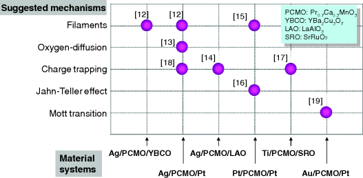
Figure 9.1 Various proposed resistive switching mechanisms for Pr0.7Ca0.3MnO3-based resistive switching devices [12–19]
Since the early exploration of the switching mechanisms of metal oxides, electronic effects have been considered as possible explanations. The dominant RRAM switching models today is based on the migration and reaction of ions or vacancies (e.g., oxygen ions or vacancies) that generates conductive paths within insulating oxides. However, several electronic effects or mechanisms may still contribute to the switching process in some RRAM materials. To categorize different RRAM switching mechanisms, the 2009 ITRS Emerging Research Device chapter classified the switching mechanisms into thermal effect, ionic effect, and electronic effect [20]. A real switching process may involve multiple effects and this classification is based on the dominant contributions. Thermal effect is related to power induced Joule heating and often involves the formation and disruption of localized conduction paths in an insulating material. Thermal effect resistive switching is usually unipolar. Ionic effect resistive switching involves the transport and electrochemical reactions of cations (e.g., Ag+, Cu+) and/or anions (e.g., O2−) and is usually bipolar switching. Cation-based ionic switching mechanism is well understood and the physical process of switching induced by ionic migration can be confirmed by microscopic imaging. However, anion-based switching is more complicated and the exact switching physics is under extensive research. This early version of RRAM categories from ERD has evolved into new forms and the so-called electronic effective RRAM is no longer a separate category in the ERD chapter. However, some electronic effects may still be involved in resistive switching process and this chapter provides a brief review of them.
The “electronic effect” covers several different mechanisms. Charge injection and trapping could modify transport characteristics and induce abrupt resistance change. Mott materials may experience several orders of magnitude of resistance change at the triggering of metal–insulator transition. Ferroelectric polarization reversal in ferroelectric oxides may cause oxide resistance change, based on which a device concept of ferroelectric tunnel junction (FTJ) has been proposed. This chapter will review these three electronic switching mechanisms and assess their potentials for memory applications. The following three sections will discuss the three electronic effects in sequence: charge injection and trapping, Mott metal–insulator transition, and ferroelectric polarization reversal.
9.2 Charge Injection and Trapping
9.2.1 Charge Trapping Induced Resistive Switching
The basic model of charge trapping resistive switching process can be described as:
- Injected charge carriers trapped inside of materials modify the band structure or interface properties, which may change transport properties and cause resistive switching.
- The release of trapped charges recovers the material to its original states.
- Retention of charge-trapping states depends on the release time of trapping charges.
The Simmons–Verderber model based on charge injection and trapping/detrapping well explained the measured switching I-V characteristics of an Au/SiO/Al structure [9]. Switching is as fast as a few nanoseconds, which was cited as evidence to relate the observed switching phenomena to electronic effects (rather than ionic or other effects involving atomic motions). It is suggested that during a “forming” process, Au ions are injected into SiO to introduce a broad band of localized impurity levels within the forbidden band of the insulator. Electrons can then move through the insulator by tunneling between adjacent sites within the impurity band. The memory effect is caused by charge (electron) storage within the insulator, which changes the band structure of the insulator and the field at the interface. The release of the trapped charge recovers the device back to its original state.
Recent publications claiming charge-trapping switching mechanisms are often based on two types of observations: (1) hysteretic I-V characteristics of a rectifying junction that can be attributed to interfacial modification by charge trapping; (2) I-V characteristics dominated by space charge limited conduction (SCLC) that is related to empty and filled trap states.
A Ti/Pr0.7Ca0.3MnO3 junction is found to be rectifying with hysteretic I-V characteristics [17]. The reversible bipolar resistive switching can be explained by the change of the width and/or height of a Schottky-like barrier, induced by trapped charge carriers in the interface states. A forming process is required before stable switching can be achieved, which may be related to the generation of oxygen defect induced states at the Ti/PCMO interface. In addition to metal/oxide junctions, hysteretic I-V characteristics are also observed in a rectifying epitaxial heterojunction SrRuO3/SrTi0.99Nb0.01O3 between two oxides, which can also be explained by charge trapping model [21].
An experiment was carefully designed to prove the interfacial switching effect by inserting a thin layer of Sm0.7Ca0.3MnO3 (SCMO) between Ti electrode and La0.7Sr0.3MnO3 (LSMO) [22]. While the Ti/LSMO interface shows no resistive switching, the insertion of SCMO of even one unit cell (uc) thickness induces resistive switching. As the thickness of SCMO increases, both hysteresis and rectification develop. Switching time also decreases from ∼10 μs for 1 uc SCMO to ∼100 ns for 5 uc SCMO. The effect of SCMO saturates after 5 uc, indicating that active layer thickness for resistive switching is several uc of SCMO adjacent to the Ti/SCMO interface.
In an Ag/Pr0.7Ca0.3MnO3/Pt structure, the hysteretic I-V characteristics can be accurately described by SCLC model; therefore, the resistive switching is linked to the transition from trap-unfilled SCLC to trap-filled SCLC [18]. Based on similar observations of SCLC-dominated I-V characteristics, charge-trapping model is adopted to explain the resistive switching behavior in Cu2O [23,24], TiOx [25], (Ba0.5Sr0.5)(Zr0.2Ti0.8)O3 [26,27], SrTiO3-δ/Nb:SrTiO3 heterojunction [28], ZrO2 [29], HfO2 [30], Gd-doped TiO2 [31], and so on. However, it should be noticed that the interpretation of the switching mechanisms in these devices may evolve over time and change with new observations.
By combining scanning electron microscopy (SEM) and electron beam induced current (EBIC) imaging with transport measurement on thin-film SrZrO3 doped with 0.2% Cr, it was shown that current conduction and switching are confined in areas localized at defects [32]. The memory effects were explained by the storage and release of charge carriers within the insulator. Similar switching is also observed in 10 μm Cr-doped single-crystal SrTiO3 [33]. Stable switching has been shown for more than 6000 write/erase cycles, with no change of signal after more than 105 readouts. Because of the existence of high initial resistance up to 100 V, it is suggested that bulk (not the interface) determines current flow across the insulator and switching originates from a change in bulk properties.
The reported switching parameters of some charge-trapping resistive switching materials reviewed in this section are summarized in Table 9.1 in Section 9.5 [9,17,18,21,22,25–27,29–32,34,35].
Table 9.1 Summary of switching characteristics of charge trapping resistive memory devices
| Devices | dI (nm) | Vsw (V) | Isw (A) | On/off ratio | Speed (s) | Retention | Cycling | References |
| Charge injection and trapping | ||||||||
| Au/SiO/Al | 20–300 | 4–8 | ∼10−2 | ∼100 | 10−9–10−7 | — | — | [9] |
| Ti/Pr0.7Ca0.3MnO3/SrTiO3 | 100 | 2–5 | ∼0.1 | 1–4 | ∼10−3 | — | — | [17] |
| SrRuO3/SrTi0.99Nb0.01O3/SrRuO3 | 100 | 2–4 | ∼10−2 | 1–100 | ∼10−4 | — | — | [21] |
| Ti/Sm0.7Ca0.3MnO3/La0.7Sr0.3MnO3 | 1–100 | 2–5 | 10−4–0.1 | >500 | ∼10−4 | — | — | [22] |
| Ag/Pr0.7Ca0.3MnO3/Pt | 150 | 1–2 | 0.1–0.01 | 10–104 | ∼10−7 | — | — | [18] |
| Al/TiOx/Ti | 10 | 3 | ∼10−3 | ∼103 | — | — | >100 | [25] |
| Pt/SrTiOx/Pt | 167 | 2–5 | 10−4 | ∼102 |
P: 5 × 10⁻⁸ E: 5 × 10⁻⁴ |
106 s at 125 °C | 105 | [34] |
| Pt/(Ba0.5Sr0.5)(Zr0.2Ti0.8)O3/Pt | 200 | 1–3 | 10−7–10−5 | ∼230 | — | — | — | [26] |
| Au/Cr/Zr+-implanted-ZrO2/n+-Si | 70 | 3–4 | ∼10−2 | ∼104 | — | >2500s | — | [29] |
| TiN/AlCu/HfO2/TiN | 20 | 0.5–1.5 | 10−2 | ∼4 | ∼5 × 10⁻⁸ | >104 s at 85 °C | >105 | [30] |
| (W or Al)/Gd:TiO2/Pt | 40 | 0.5–2 | ∼10−2 | ∼103 | — | — | >10 | [31] |
| Pt/SrZrO3(0.2% Cr)/SrRuO3 | 35 | — | ∼10−4 | 45–90 | — | ∼5 × 10⁴ s | — | [32] |
| Al/SiOx/p-Si/Al | 5–7 | ∼2 | — | ∼102 | — | >2000s | >103 | [35] |
| Mott transition | ||||||||
| Au/Pr0.7Ca0.3MnO3/Pt | 360 | ∼0.8 | 10−2–10−1 | ∼10 | — | — | — | [19] |
| Ag/CeO2/La0.67Ca0.33MnO3 | 80 | 2–4 | ∼10−2 | 102–104 | — | — | — | [46] |
| Pt/TiO2/TiN/Pt | 2.5 | ∼2 | — | >102 | 2 × 10⁻⁸ | — | >10 | [48,49] |
| Au/VO2 (sol-gel)/Au | 200 | >50 | 6 × 10⁻⁴ | ∼103 | — | — | >108 | [52] |
| Au/VO2 (anodic oxidation)/Au | 200 | 1–10 | 10−5–10−4 | — | 10−9–10−4 | — | — | [51] |
| Au/Cr/VO2 (epitaxy)/Cr/Au | ∼90 | 10–20 | ∼10−2 | — | — | — | — | [53] |
| Ferroelectrical polarization reversal | ||||||||
| Au/PbTiO3/La0.5Sr0.5CoO3 | 200 | 2–4 | 10−6–10−4 | ∼102 | <10−2 | — | — | [65] |
| Pt/Pb(Zr0.52Ti0.48)O3/SrRuO3 | 4–6 | 0.5–1 | ∼10−4 | ∼4 | — | — | — | [67] |
| Pt/SrTiO3/Pt | 4.5 | ∼0.8 | ∼10−2 | — | — | Unspecified extended period | — | [68] |
| BaTiO3 (probed by PFM) | 1–50 | ∼3 | — | 2–103 | — | — | — | [70] |
| Au/Co/BaTiO3/La0.67Sr0.33MnO3 | 500 | ∼2 | ∼10−5 | 102 | 10−8 | — | >900 | [71] |
| P(VDF:70%-TrFE:30%) | 2 mono-layer | <1 | — | ∼6 | — | — | — | [73] |
9.2.2 Charge-Trapping Resistive Switching Memory Performance
Scaling: Since charge-trapping mechanism involves defects or charge trapping centers, fluctuation or inhomogeneity of the defect density may limit the scalability of these devices. A defect modification model suggests a statistical size limit on the order of 10–100 nm [36]. Localized conduction and switching are also observed in some charge-trapping resistive switching devices [32], which are often considered evidence of promising scalability. Fundamentally, the size limit of these localized conduction and switching region is still subject to the density fluctuation of the trapping sites.
Speed: The write/erase speed depends on how fast the charge trapping/detrapping processes take place. Reported speed in literature varies from tens of μs to several ns. Slow measured speed could be attributed to parasitic RC delay in large device structures. An electronic effect switching process may occur in tens of nanosecond or shorter time [21]. However, the feasibility of sub-nanosecond operation in large arrays is unclear. Tradeoff between the on/off ratio and switching speed is observed in Ti/PCMO [17] and Ag/PCMO [18]. The study on the switching in SiOx shows a “dead time” (from tens of milliseconds up to several seconds) that prevents immediate repeating of cycles [9]. If such a dead time exists, memory access algorithms need to be designed accordingly to minimize delay. The reading speed of a charge-trapping resistive switching device is determined by peripheral circuitry. With a few orders of magnitude on/off ratio in these devices, reading is unlikely to be a concern, as long as reading voltage is not high enough to disturb device states.
On/off ratio: On/off ratio is determined by the resistance difference between the charge-trapped state and the charge-released state. The ratio could vary in a large range depending on trap-controlled conduction mechanisms. Ratios from<10 up to 105 have been reported. The on/off ratio in some devices was found to decrease with shorter switching pulse width, which presents a performance trade-off. A high on/off ratio helps to expedite reading and reduce errors.
Retention: Retention depends on the release time of trapped charges [18], which may depend exponentially on the trap depth or some activation energies [23]. Some estimation has shown that 10-year retention at room temperature is achievable for activation energy of 1.0–1.1 eV. Charge-trapping resistive switching materials may be engineered to achieve 10-year retention, but tradeoffs may exist between retention and other switching parameters. Retention of 1600 minutes at 85 °C has been measured on PCMO [12].
Endurance: The endurance of charge-trapping devices is limited by the stability of defects and trapping sites. A microscopic imaging study of localized switching process shows variation of the conduction/switching sites that indicates defect generations during switching [33]. Cycling fatigue due to defect generation is also observed in Pt/PCMO/Pt devices after 104 cycles [37].
Switching energy: In principle the minimum switching energy is associated with the trap depth; however, in reality much higher energy is required to switch these devices. The switching energy (E) can be estimated from the measured switching voltage (V), switching current (I) and switching time (t), that is, E = V·I·t. As an example, the switching parameters for AlCu/HfO2/TiN are V ≈ 1.5 V, I ≈ 0.3 mA, and t ≈ 50 ns, which results in E ≈ 2 × 10⁻¹¹ J/bit [31]. This demonstrated switching energy is in a typical range for resistive switching materials. It has been shown that switching voltage, current, and time can be further reduced from the values chosen above by material engineering and device optimization. Switching energy smaller than 10−12 J/bit appears feasible for charge-trapping resistive switching memories.
CMOS compatibility: Some resistive switching memories, including these based on charge-trapping mechanisms have been integrated in standard CMOS structure [11,23,38]. Some novel materials used in charge-trapping resistive switching devices have been shown to be compatible with Si CMOS process. The simple two-terminal structure of resistive switching devices makes it easy for integration in CMOS without area penalty (e.g., at via locations). In the 1-transistor-1-resistor (1T1R) memory structure, it is the selection transistors that limit memory scalability.
Analysis has shown that for charge-trapping switching mechanism there exists a tradeoff between switching speed and retention [39]. Sufficiently high trap depth or barrier height is required to suppress the escape of the trapped charges to achieve long retention; however, high barriers constrain the magnitude of current density required for fast reading and switching.
9.3 Mott Transition
9.3.1 Resistive Switching Induced by Mott Transition
Charge injection into some materials may induce a transition from strongly correlated to weakly correlated electrons, leading to a Mott metal–insulator transition [40–44]. Resistive switching may occur as a result of this transition.
An observation on the electrical trigger of resistive switching in magnetoresistive manganite PCMO at low temperature suggests the possibility of dielectric breakdown of the charge-ordered state in Mott insulators [45]. In the bipolar resistive switching observed in Au/Pr0.7Ca0.3MnO3/Pt structure at room temperature, the mixed valence state Mn4+/Mn3+ at the Au/PCMO interface is found critical for switching [19]. No resistive switching is observed at Au/PMO interface with only Mn3+ valence state or at Au/CMO interface with only Mn4+ valence state. An increase of Mn4+/Mn3+ ratio caused by oxygen annealing results in increasing HRS/LRS resistance ratio. It is postulated that the mixed Mn4+/Mn3+ valence states at the metal/PCMO interface can regulate current through metal–insulator transition induced by a critical carrier density modulated by electrostatic doping, which leads to resistive switching.
Similarly, bipolar resistive switching observed in an Ag/CeO2/L0.67Ca0.33MnO3 structure is also explained by mixed valence states of Ce4+/Ce3+ and Mott transition [46]. The on/off ratio reaches 105. Electrical field initiates the process of oxygen migration and the formation of oxygen vacancies facilitates the shift in the valence state of Ce cations. Such a valence shift of cerium oxide may propagate and self-assemble under the applied electric field through the insulator until a conductive percolation path of neighboring Ce3+ sites is created when some critical density of valence shifted sites is reached. The use of conductive oxide LCMO as the bottom electrode ensures free oxygen migration through the CeO2/LCMO interface.
In a 0.2 mol% Cr-doped SrTiO3 resistive switching material, x-ray absorption near-edge structure (XANES) spectra reveals significant valence change of Cr from Cr3+ to Cr4+ during electrical forming process [47]. It is suggested that the resistance change in Cr:SrTiO3 is caused by Mott transition associated with internal doping of the Ti 3d band due to a change of Cr-dopant valence.
Mott transition is also proposed as the mechanism for the bipolar resistive switching observed in a 2.5 nm anatase TiO2 layer grown by oxidation of a TiN diffusion barrier [48,49]. Mott transition may be triggered by the increase in donor concentration caused by the electron injection from the top electrode (Pt), which is accompanied by oxygen vacancy formation and O2− migration in the anatase TiO2 layer. Devices can be switched within 20–30 ns with ∼2 V voltage pulses. The on/off ratio reaches almost 400.
Vanadium oxide (VO2) is a well-known Mott material with potentials for high-speed device applications [50–57]. Sharp resistance change can be triggered by temperature [50,54,55] or current/voltage [51–53,56]. The metal–insulator transition is often accompanied by thermal structural phase transition (SPT), which complicates the switching mechanism and degrades device performance [53]. However, study has shown that thermal effect alone cannot describe the transition and electron correlation effects also contribute to the metal–insulator transition in VO2 [51,57]. With careful design of device geometry, material parameters and thermal condition, it may be possible to induce electronic transition without triggering thermal SPT [53,57].
The transition time of VO2 is shown to be dependent on voltage and can be as short as 1.5 ns [51]. The fundamental limit of the transition time may be on the order of ps [51]. On/off ratio is usually on the order of 103–105. Endurance as long as 108 cycles has been observed on sol-gel VO2 film [52], and on sputtered VO2 thin-film ∼100 switching cycles is also measured [54]. Some studies also show chaotic switching behaviors inside the hysteresis region near the onset of the transition [55]. Although material properties at nano-scale may differ drastically from those of bulk materials, switching characteristics of devices as small as 200 nm in diameter are found to be similar to that of larger devices [56].
The reported values of switching parameters of the Mott transition devices discussed above are summarized in Table 9.1 [19,46,48,49,51–53].
Mott transition is incorporated in a phenomenological model that describes an insulating medium as a nonpercolative structure of bulk domains and electrode/insulator interface as smaller domains. Mott transition due to strong electron correlation at the interface plays a key role for switching [58,59]. Another model for resistive switching (colossal electro-resistance) is developed based on interface Mott transition using the density matrix renormalization group (DMRG) method [60].
In addition to the usual two-terminal structure, Mott transition based nonvolatile memory may also be built in a three-terminal transistor structure, where a Mott transition layer is included in the gate stack to allow or block tunneling current into a charge trapping layer [61]. In another proposed transistor concept based on Mott transition, additional carriers are drawn into the channel electrostatically from source/drain by gate voltage to induce Mott transition and create a thin conducting layer at the interface [62,63]. It is suggested that Mott transition field-effect transistors can overcome some intrinsic limitations of Si MOSFET, such as lower carrier/dopant fluctuations and lower gate leakage.
9.3.2 Mott Transition Resistive Switching Memory Performance
Scaling: Properties of Mott transition materials in nano-scale may differ drastically from the properties of bulk materials [64]. Although switching devices on the scale of 200 nm has been shown to have the characteristics similar to these observed in larger devices, this size is much larger than competitive sizes of state of the art memory technologies. More research on the size effect of the Mott transition properties is needed to address the fundamental scaling limit of this type of devices.
Speed: Switching speed as short as 1.5 ns has been observed on VO2 [51], and TiO2-based devices can be switched with 20–30 ns pulses [48,49]. Since the transition is driven by electron–electron correlations, the fundamental speed limit is expected to be on the order of ![]() ·ρ where
·ρ where ![]() is the high-frequency dielectric constant and ρ is the specific resistivity of the material [51]. This value is on the order of 10−12 s, equivalent to a frequency limit of 1 THz.
is the high-frequency dielectric constant and ρ is the specific resistivity of the material [51]. This value is on the order of 10−12 s, equivalent to a frequency limit of 1 THz.
On/off ratio: Experiments have shown on/off ratio in the range of 103–105 on Mott transition devices [46,54]. This is comparable with charge-trapping and ferroelectric resistive switching devices.
Retention: Although retention has been shown in some materials associated with Mott transition, the retention mechanism needs further study. The electrical conditions that triggered the Mott transition have to be continuously present to sustain the transition states for retention, for example, by ferroelectric field or charge trapping [47]. Notice that the volatile switching due to Mott transition may also be utilized as memory select devices.
Endurance: Endurance as long as 108 cycles has been shown on VO2-based switching devices [51]. Without structural change, electrically triggered Mott transition is expected to have long endurance.
Switching energy: A rough estimation of switching energy can be made using the reported data on Pt/TiO2/TiN [48,49]. Reset switching can be done with 2.2 V, 30 ns pulses and LRS has the resistance of 0.2 kΩ. The switching energy is estimated to be E = V2/R·t ≈ 7 × 10⁻¹⁰ J/bit, a relatively high value due to large current. Lower switching energy may be achievable with improved materials and devices.
9.4 Ferroelectric Resistive Switching
9.4.1 Ferroelectric Resistive Switching Mechanism
If the “insulator” layer in the MIM structure is made of ferroelectric materials, ferroelectric polarization can modify the carrier transport characteristics and induce bistable resistive switching. It should be noted that unlike Ferroelectric RAM (FeRAM) where ferroelectric materials are used as capacitors, ferroelectric resistive switching memory operates based on the transport property across a ferroelectric layer which can be electrically modulated due to ferroelectric polarization reversal.
In an Au/PbTiO3/La0.5Sr0.5CoO3 Schottky diode with ferroelectric PbTiO3 layer, the interface charge and the band diagram can be continuously and permanently modified by an external electric field [65]. Bistable I-V behaviors are observed during voltage sweep, where the threshold voltage for set switching from HRS to LRS is related to the coercive field. The thickness of PbTiO3 layer is 0.2 μm, and HRS conduction is found to be either bulk controlled (SCLC) or electrode controlled (Schottky emission), depending on the direction and history of the applied electric field. The changing conduction mechanisms are related to the polarization dependence of the band bending and depletion region width, which is caused by the local field-dependent permittivity of the ferroelectric material. The Schottky barrier width is reduced (increased) when the polarization in the space–charge region of the diode is parallel (anti-parallel) to the internal electric field. Therefore, the resistive switching can be explained by the change of the Schottky barrier width caused by abrupt change of the polarization at coercive field.
If the ferroelectric layer is made thin enough to allow carrier tunneling, the tunneling property of the ferroelectric layer may also be modified electrically, leading to a new device concept named “ferroelectric tunnel junction” (FTJ) [66]. The electric field induced polarization reversal of a ferroelectric barrier may have pronounced effect on the conductance of FTJs. The polarization reversal changes the sign of the polarization charge at the barrier/electrode interface, the positions of ions in ferroelectric unit cells, and lattice strains inside the barrier [66].
In a resistive switching heteroepitaxial junction Pt/Pb(Zr0.52Ti0.48)O3/SrRuO3, the switching voltage matches well with the coercive electric field, suggesting the polarization reversal in the ferroelectric barrier as the origin of the resistive switching phenomena [67]. However, recent experiments suggest the possibility of ionic contributions in the switching process in these devices. Resistive switching observed in a junction between Pt electrode and ultrathin SrTiO3 (4.5 nm) is also attributed to ferroelectric polarization [68]. Although bulk, undoped SrTiO3 is not ferroelectric, epitaxial SrTiO3 thin film may show strain-induced ferroelectricity [69].
Robust ferroelectricity and resistive switching in highly strained ultra thin BaTiO3 (down to 1 nm thickness) are demonstrated by piezoresponse force microscopy (PFM) and conductive tip atomic force microscopy (CTAFM) [70]. The measured tunnel electro-resistance (TER, i.e., on/off ratio) increases from ∼200% at the thickness of 1 nm to ∼75 000% at 3 nm. The observed thickness dependence of the TER suggests that the ferroelectric resistive switching is caused by the polarization induced changes of the tunnel barrier characteristics (height, thickness, tunneling mass, etc.) rather than the changes in the density of states (DOS) at the barrier–electrode interface. Scalability of ferroelectric resistive switching in BaTiO3 is demonstrated down to device as small as 70 nm. A FTJ device with Au//Co/BaTiO3/La0.67Sr0.33MnO3 structure and diameter of 500 nm is fabricated and characterized [71,72]. It demonstrates on/off ratio as high as 100, low switching current of ∼1 × 10⁴ A/cm2, endurance over 900 cycles, and switching speed faster than 10 ns.
Resistive switching induced by polarization reversal is also observed on ferroelectric polymers [73,74]. The tunneling current measured by scanning tunneling spectroscopy (STS) on a two monolayer thick ferroelectric copolymer of VDF:70%-TrFE:30% (vinylidene fluoride with trifluoroethylene) can change more than six times when flipping the polarity of probing voltage [73]. This local “switching” of vertical conductance can be explained by rotation of the top layer polarization direction.
Some reported key switching parameters of the ferroelectric resistive switching devices discussed here are summarized in Table 9.1 [65,67,68,70,71,73].
The resistive switching characteristics can be quantitatively described by theoretical models [75–77]. The change of potential profile at different polarization directions in a FTJ structure could lead to significant resistance change and calculation shows that electro-resistance (i.e., on/off ratio) of FTJs can be as high as 103 [75]. Another FTJ model is developed based on strain-induced changes of the barrier thickness, electron effective mass, and conduction band edge at the coercive field [76]. The model predicts that asymmetric FTJs with dissimilar top and bottom electrodes have larger on/off ratio than symmetric FTJs.
More novel device concepts may be developed by combining ferroelectrics and ferromagnetism. It is found that resistance of a ferroelectric/ferromagnetic LiNbO3/La0.69Ca0.31MnO3 junction can be tuned by both magnetic field and electric field [78]. The voltage pulse induced resistive switching is attributed to ferroelectric polarization at the junction interface. Combining ferromagnetic electrodes with a ferroelectric tunnel barrier may produce multiferroic tunnel junctions (MFTJ). A four-state resistive switching device concept built on magnetic tunnel junctions with ferroelectric barriers is predicted based on first-principles calculations [79]. A Fe/BaTiO3/La0.67Sr0.33MnO3 structure was used to experimentally demonstrate local, large, and nonvolatile control of spin polarization by ferroelectric polarization reversal [80].
A critical requirement for functional FTJs is the existence of ferroelectricity in nanometer thick barrier materials [66]. Ferroelectricity is a cooperative phenomenon; therefore, it is generally expected that there is a critical thickness (tc) below which ferroelectricity collapses due to the depolarization field or finite size effects [81–84]. Recent theoretical and experimental studies have shown that either tc could be really small (a few unit cells) or there is essentially no intrinsic ferroelectric size limit for practical devices [83–96]. Figure 9.2 summaries the reported tc on some ferroelectric materials. These results indicate that FTJ devices with ultrathin ferroelectric layer (down to a couple of nm thickness) are feasible.
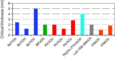
Figure 9.2 Reported critical thickness of some ferroelectric materials [83–96]
Major challenges still exist before FTJ or MFTJ can be implemented in device applications. For example, parasitic effects such as local conductivity and transport via localized states must be eliminated. Better understanding is needed regarding the mechanisms of domain formation, nucleation and switching in nanoscale ferroelectrics, and tunneling transport across polar thin film dielectrics [66].
9.4.2 Ferroelectric Resistive Switching Memory Performance
Resistive switching memory based on FTJ is an emerging area with many open questions, especially ferroelectric properties in nano-scale. Interestingly, much of the nano-ferroelectric domain behavior can be derived from bulk classical physics [96]. In addition, extensive research results are available for FeRAM and may provide useful references for the research on ferroelectric resistive switching memory [97,98].
Scaling: Numerous studies on finite size effects in ferroelectrics point to a critical particle size or film thickness below which ferroelectricity disappears [99]. This critical size may impose a scaling limit on ferroelectric resistive switching devices. It has been shown that ferroelectricity may persist in films as thin as a few nanometers. Achievable memory density is determined by lateral size limit. A study on self-assembly PbTiO3 and Pb(ZrxTi1−x)O3 nano-grains shows that ferroelectricity is preserved down to grain size of 20 nm [100]. Furthermore, BaTiO3 nanowires as small as 10 nm in diameter are shown to retain ferroelectricity [101]. Therefore, it seems feasible to scale ferroelectric resistive switching devices below 10 nm.
Speed: Switching speed of ferroelectric resistive switching memory is determined by the ferroelectric polarization reversal time. The reversal switch typically takes place by the generation of new reverse domains at particularly sites [98], whose rate in submicron ferroelectrics is limited by nucleation rather than by domain wall motion and can be less than 1 ns [96]. Switching speed shorter than 4 ns has been measured in LiTaO3 nano-domains using scanning nonlinear dielectric microscopy (SNDM) [102]. In FeRAM technology, access time as small as 280 ps has been tested in laboratory [98].
On/off ratio: On/off ratio of ∼102 has been demonstrated on Schottky diode made on thicker PbTiO3 film [65] and the ratio could be even higher in ultrathin BaTiO3 [70]. Although it has been shown that the on/off ratio decreases with the thickness of the ferroelectric tunnel barriers, a ratio of nearly 103 can be achieved with a 3 nm tunnel barrier [70,75].
Retention: Destabilization of the ferroelectric polarization state may cause the loss of information recorded in ferroelectric resistive switching memory. For example, oxygen migration under the depolarization field or other built-in field may cause retention degradation [98,103]. Nonvolatility of nano-scale ferroelectric thin film has been proven by experiments, for example, ferroelectric state in a 4 nm Pb(Zr0.2Ti0.2)O3 film is stable for over 140 h [93]. The retention time of induced polarization in BaTiO3 nanowires exceeds 5 days [98]. Some ferroelectric field effect devices have shown retention of 1–2 weeks or even over 10 months at room temperature [104–106]. Under optimal conditions, retention of ferroelectric memories may exceed 10 years at room temperature [97].
Cycling endurance: Ferroelectric memories have shown excellence endurance of 1011–1012 cycles [107–109]. Data projection predicts endurance longer than 1016 cycles [108]. The cycling limit may be imposed by polarization fatigue, that is, the reduction of switchable ferroelectric polarization by repetitive electrical cycling [98]. Further study is needed to understand the endurance failure in nano-scale ferroelectric films.
Switching energy: Switching voltage of ferroelectric resistive switching memory is related to the coercive field that has been shown to decrease with the film thickness into the nanometer range [67,96]. This is desirable for low-voltage, low-power memory applications. Switching energy <10 fJ/bit is estimated based on measured characteristics of Au//Co/BaTiO3/La0.67Sr0.33MnO3 FTJ devices [71].
9.5 Perspectives
Resistive switching memories have presented promising opportunities and also great challenges. In the category of electronic effect resistive switching, there are wide range of materials with different switching mechanisms and characteristics. The exact switching processes and device physics are still not clearly understood. Some of the claimed mechanisms for the reported devices discussed in this chapter may be found to be incomplete or even incorrect with further investigations.
Table 9.1 summarizes reported parameters of the three types of electronic effect resistive switching memories. Notice that some parameters (e.g., speed) may be significantly below the best achievable values due to parasitic effects. Charge injection and trapping are well known processes in semiconductor device physics and are adopted to explain many resistive switching phenomena. Fewer examples of switching devices based on Mott transition and ferroelectric polarization reversal have been reported, partially due to the difficulty of conclusively attributing a switching phenomenon to these mechanisms. Some intriguing research on these switching mechanisms and device application is based on theoretical modeling. For example, resistive switching is predicted in a two-dimensional electron gas (2DEG) induced by ferroelectric reversal in oxide LaAlO3/SrTiO3 heterostructures, which may allow device scaling down to several nanometers [110]. Figure 9.3 summarizes the measured switching current vs. voltage of these devices, with different colors for different types of electronic effects: charge trapping (blue), Mott transition (orange), and ferroelectric reversal (pink). Figure 9.4 plots the measured on/off ratio versus switching speed of these devices.

Figure 9.3 Reported switching current versus voltage of electronic-effect resistive switching devices. Blue: charge trapping; orange: Mott transition; pink: ferroelectric reversal. Sizes of the symbols have no physical meaning and are varied to differentiate the three mechanisms (Color in electronic version)
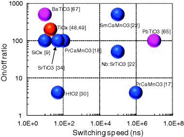
Figure 9.4 Reported on/off ratio versus switching speed of electronic-effect resistive switching devices. Blue: charge trapping; orange: Mott transition; pink: ferroelectric reversal (Color in electronic version)
In any binary switching devices for information representation and storage, some physical changes have to occur in the material to enable the transition between two distinguishable states. Intuitively one can expect that the switching involving only electronic changes (e.g., electron spin flipping, charge motion, injection, and trapping, etc.) may consume lower power, switch faster, and have longer endurance than changes involving atomic/ionic motions (e.g., mass transport, ionic migration, electrochemical reactions, etc.) In this sense, electronic effect resistive switching memory may have certain advantages over the switching devices based on thermally induced physical changes (e.g., phase change memory) or ionic motions (e.g., ionic effect memory).
An important requirement for emerging nonvolatile memories is the scalability superior to Flash memories. As discussed earlier, the scaling of charge-trapping memories is limited by the fluctuation or inhomogeneity of the defect density. Ferroelectricity is a collective phenomenon; therefore, it is expected that the size of switching devices due to ferroelectric reversal has to be large enough for the material to remain ferroelectric. However, this ferroelectric size limit has been shown to be as small as a few nanometers. The scaling limit of Mott transition still requires more study, but there does not appear to be a fundamental size limit. Overall, it appears that electronic effect RRAM devices can be scaled to several nanometers.
With the current memory technologies already at <45 nm technology nodes, increasing memory density by device scaling alone offers limited potential. Multi-level cell (MLC) design and 3D stackable structures provide more growth space for high-density memories. For devices with high on/off ratios and cumulative switching mechanisms (e.g., charge trapping), it may be possible to program devices to multiple levels by accurately controlling the resistance levels. FTJ-based devices are not a natural choice for MLC, because of the binary nature of ferroelectric polarization. However, the MFTJ discussed in Section 9.4.1 may enable MLC by combining ferroelectrics and ferromagnetism in one device. 3D stackable memories still face key challenges in memory select device.
Table 9.2 qualitatively summarizes the three electronic effect resistive switching memories and their potentials for the next-generation nonvolatile memories. Table 9.3 summarizes reported values of some key switching parameters for the three mechanisms reviewed in the paper.
Table 9.2 Summary of three electronic resistive switching mechanisms
| Types | Charge trapping | Mott transition | Ferroelectric |
| Data representation | Resistance change due to different transport properties of trap filled and trap empty states | Resistance change due to different transport properties of metallic and insulating states of Mott insulators | Resistance change due to different transport properties of ferroelectric tunnel layer at opposite polarization |
| Switching mechanism | Field-controlled trap filling and detrapping | Carrier injection induced Mott transition | Field-controlled polarization reversal |
| Scaling limit | Statistic fluctuation of defects and traps | Highly scalable, for example, interface 2DEG | Ferroelectric size effect; scalable to <10 nm |
| Multi-level cell capability | Possible; require accurate control of trap filling process | Probably difficult because of high sensitivity to small parameter change | Unlikely for ferroelectric tunnel junction (FTJ); possible with multiferroic tunnel junction (MFTJ) |
| CMOS compatibility | Compatible | Compatible | Compatible |
| Cross-bar compatibility | Prefer rectifying and nonlinear I-V, high on/off ratio; may require selection devices | Require high on/off ratio and asymmetric I-V; may require selection devices | Require high on/off ratio; may require selection devices |
Table 9.3 Electronic effect resistive switching memory performance metrics
| Charge trapping | Mott transition | Ferroelectric | |
| Cell element | 1 T-1R, 1D-1R | 1 T-1R, 1D-1R | 1 T-1R, 1D-1R |
| Scaling limit (nm) | 10–100 | <200 | ≤10 |
| On/off ratio | ≥102 | ≥103 | ≥103 |
| W/E time (ns) | <50 | ≤1 (1.5 ns demonstrated) | ≤4 |
| Retention time | 10 yr (1600 min at 85 °C demonstrated) | — | 10 yr (140 h demonstrated) |
| Cycling endurance | >104 cycles | >108 cycles | >1012 cycles |
| W/E voltage (V) | 1–5 | ≤1 | ≤1 |
| Read voltage (V) | <1 | ≤1 | <1 |
| Write energy (J/bit) | <1 × 10⁻¹¹ | <10−10 | <1 × 10⁻¹¹ |
| Challenges | Defect fluctuation; material stability | Possible structural change; thermal stability | Ferroelectric fatigue |
As a final note, a unique advantage of electronic effect resistive switching memory may lie in the large variety of materials and mechanisms. The combination of different materials and switching physics may provide innovative approaches to engineer the switching process to achieve better device performance. For example, the insertion of ferroelectric PZT layer at the interface of an Ag/PCMO junction enhances the switching effects and improves device characteristics [111]. The combination of a ferroelectric layer and a ferromagnetic layer in the LiNbO3/La0.69Ca0.31MnO3 junction may create multiferroic functionalities [78]. The prerequisite is clear understanding of these different mechanisms and the ability to differentiate and control these different processes.
9.6 Summary
This chapter reviews three electronic effects that may contribute to resistive switching mechanisms in oxide-based RRAM devices: charge injection and trapping, Mott metal–insulator transition, and ferroelectric reversal. Recent research on RRAM switching mechanisms has converged to ionic reaction and migration that induce the formation and rupture of filamentary conductive paths. Pure electronic effects have been considered less likely to dominate the switching process. However, various electronic effects may still contribute partially to the switching process. For Mott materials and ferroelectric oxides, metal–insulator transition and ferroelectric reversal are possible mechanisms that trigger switching processes. Although the classification of the electronic effect mechanisms is somewhat subjective, evidence of electronic effect switching process is continuously reported in literature. Exploring these potential electronic effect mechanisms is still valuable for the understanding of the complex resistive switching process in RRAM devices.
References
- 1. Pagnia, H. and Sotnik, N. (1988) Bistable switching in electroformed metal-insulator-metal devices. Physica Status Solidi (a), 108, 11–65.
- 2. Dearnaley, G., Stoneham, A.M., and Morgan, D.V. (1970) Electrical phenomena in amorphous oxide films. Reports on Progress in Physics, 33, 1129–1191.
- 3. Oxley, D.P. (1977) Electroforming, switching and memory effects in oxide thin films. Electrocomponent Science and Technology, 3, 217–224.
- 4. Ansari, A.A. and Qadeer, A. (1985) Memory switching in thermally grown titanium oxide films. Journal of Physics D: Applied Physics, 18, 911–917.
- 5. Argall, F. (1968) Switching phenomena in titanium oxide thin films. Solid-State Electronics, 11, 535–541.
- 6. Bruyere, J.C. and Chakraverty, B.K. (1970) Switching and negative resistance in thin films of nickel oxide. Applied Physics Letters, 16(1), 40–43.
- 7. Hickmott, T.W. (1965) Electron emission, electroluminescence, and voltage-controlled negative resistance in Al-Al2O3-Au diodes. Journal of Applied Physics, 36(6), 1885–1896.
- 8. Hiatt, W.R. and Hickmott, T.W. (1965) Bistable switching in niobium oxide diodes. Applied Physics Letters, 6(6), 106–108.
- 9. Simmons, J.G. and Verderber, R.R. (1967) New conduction and reversible memory phenomena in thin insulating films. Proceedings of the Royal Society A, 301, 77–102.
- 10. Beck, A., Bednorz, J.G., Gerber, Ch. et al. (2000) Reproducible switching effect in thin oxide films for memory applications. Applied Physics Letters, 77(1), 319–321.
- 11. Baek, I.G., Lee, M.S., Seo, S. et al. (Dec. 2004) Highly scalable non-volatile resistive memory using simple binary oxide driven by asymmetric unipolar voltage pulses, IEDM Tech. Dig., pp. 587–560.
- 12. Liu, S.Q., Wu, N.J., and Ignatiev, A. (2000) Electric-pulse-induced reversible resistance change effect in magnetoresistive films. Applied Physics Letters, 76(19), 2479–2481.
- 13. Nian, Y.B., Strozier, J., Wu, N.J. et al. (2007) Evidence for an oxygen diffusion model for the electric pulse induced resistance change effect in transition-metal oxides. Physical Review Letters, 98(14), 146403–146406.
- 14. Tsui, S., Baikalov, A., Cmaidalka, J. et al. (2004) Field-induced resistive switching in metal-oxide interfaces. Applied Physics Letters, 85(2), 317–319.
- 15. Fujimoto, M., Koyama, H., Kobayashi, S. et al. (2006) Resistivity and resistive switching properties of Pr0.7Ca0.3MnO3 thin films. Applied Physics Letters, 89(24), 2435041-3.
- 16. Hsu, S.T., Li, T., and Awaya, N. (2007) Resistance random access memory switching mechanism. Journal of Applied Physics, 101(2), 024517-1-8.
- 17. Sawa, A., Fujii, T., Kawasaki, M., and Tokura, Y. (2004) Hysteretic current–voltage characteristics and resistance switching at a rectifying Ti/Pr0.7Ca0.3MnO3 interface. Applied Physics Letters, 85(18), 4073–4075.
- 18. Odagawa, A., Sato, H., Inoue, I.H. et al. (2004) Colossal electroresistance of a Pr0.7Ca0.3MnO3 thin film at room temperature. Physical Review B-Condensed Matter, 70(22), 224403-1-4.
- 19. Kim, D.S., Kim, Y.H., Lee, C.E., and Kim, Y.T. (2006) Colossal electroresistance mechanism in a Au/Pr0.7Ca0.3MnO3/Pt sandwich structure: Evidence for a Mott transition. Physical Review B-Condensed Matter, 74(17), 174430-1-6.
- 20.International Roadmap Committee (2009) Emerging Device Research Chapter, in the International Technology Roadmap of Semiconductors.
- 21. Fujii, T., Kawasaki, M., Sawa, A. et al. (2005) Hysteretic current–voltage characteristics and resistance switching at an epitaxial oxide Schottky junction SrRuO3/SrTi0.99Nb0.01O3. Applied Physics Letters, 86(1), 012107-1-3.
- 22. Sawa, A., Fujii, T., Kawasaki, M., and Tokura, Y. (2006) Interface resistance switching at a few nanometer thick perovskite manganite active layers. Applied Physics Letters, 88(23), 232112-1-3.
- 23. Chen, A., Haddad, S., Wu, Y.C. et al. (Dec. 2005) Non-volatile resistive wwitching for advanced memory applications, IEDM Tech. Dig., pp. 765–768.
- 24. Chen, A., Haddad, S., Wu, Y.C. et al. (2007) Switching characteristics of Cu2O metal-insulator-metal resistive memory. Applied Physics Letters, 91(12), 123517-1-3.
- 25. Yu, L., Kim, S., Ryu, M. et al. (2008) Structure effects on resistive switching of Al/TiOx/Al devices for RRAM applications. IEEE Electron Device Letters, 29(4), 331–333.
- 26. Xia, Y., He, W., Chen, L. et al. (2007) Field-induced resistive switching based on space-charge-limited current. Applied Physics Letters, 90(2), 022907-1-3.
- 27. Xia, Y., Liu, Z., Wang, Y. et al. (2007) Conduction behavior change responsible for the resistive switching as investigated by complex impedance spectroscopy. Applied Physics Letters, 91(10), 102904-1-3.
- 28. Ni, M.C., Guo, S.M., Tian, H.F. et al. (2007) Resistive switching effect in SrTiO3-δ/Nb-doped SrTiO3 heterojunction. Applied Physics Letters, 91(18), 183502-1-3.
- 29. Liu, Q., Guan, W., Long, S. et al. (2008) Resistive switching memory effect of ZrO2 films with Zr+ implanted. Applied Physics Letters, 92(1), 012117-1-3.
- 30. Lee, H., Chen, P., Wu, T. et al. (Apr. 2008) HfO2 bipolar resistive memory device with robust endurance using AlCu as electrode, VLSI-TSA, pp. 146–147.
- 31. Liu, L.F., Tang, H., Wang, Y. et al. (Oct. 2006) Reversible resistive switching of Gd-doped TiO2 thin films for nonvolatile memory applications, Inter. Conf. Sol. State and Inter. Circ. Tech. (ICSICT), pp. 833–835.
- 32. Rossel, C., Meijer, G.I., Brémaud, D., and Widmer, D. (2001) Electrical current distribution across a metal–insulator–metal structure during bistable switching. Journal of Applied Physics, 90(6), 2892–2894.
- 33. Watanabe, Y., Bednorz, J.G., Bietsch, A. et al. (2001) Current-driven insulator–conductor transition and nonvolatile memory in chromium-doped SrTiO3 single crystals. Applied Physics Letters, 78(23), 3738–3740.
- 34. Choi, D., Lee, D., Sim, H. et al. (2006) Reversible resistive switching of SrTiOx thin films for nonvolatile memory applications. Applied Physics Letters, 88(8), 082904-1-3.
- 35. Tsai, C., Chang, T., Liu, P. et al. (2008) Low temperature improvement on silicon oxide grown by electron-gun evaporation for resistance memory applications. Applied Physics Letters, 93(5), 052903-1-3.
- 36. Tsui, S., Wang, Y.Q., Xue, Y.Y., and Chu, C.W. (2006) Mechanism and scalability in resistive switching of metal-Pr0.7Ca0.3MnO3 interface. Applied Physics Letters, 89(12), 123502-1-3.
- 37. Papagianni, C., Nian, Y.B., Wang, Y.Q. et al. (Nov. 2004) Impedance study of reproducible switching memory effect, Non-Volatile Memory Tech. Workshop, pp. 125–128.
- 38. Zhuang, W.W., Pan, W., Ulrich, B.D. et al. (Dec. 2002) Novell colossal magnetoresistive thin film nonvolatile resistance random access memory (RRAM), IEDM Tech. Dig., pp. 193–196.
- 39. Schroeder, H., Zhirnov, V.V., Cavin, R.K., and Waser, R. (2010) Voltage-time dilemma of pure electronic mechanisms in resistive switching memory cells. Journal of Applied Physics, 107(5), 054517-1-8.
- 40. Mott, N.F. (1968) Metal-insulator transition. Reviews of Modern Physics, 40, 677.
- 41. Mott, N.F. (1982) Review lecture: metal-insulator transitions. Proceedings of the Royal Society A, 382, 1–24.
- 42. Imada, M., Fujimori, A., and Tokura, Y. (1998) Metal-insulator transitions. Reviews of Modern Physics, 70(4), 1039–1263.
- 43. Edwards, P.P., Johnston, R.L., Rao, C.N.R. et al. (1998) The metal-insulator transition: a perspective. Philosophical Transactions of the Royal Society of London A, 356(1735), 5–22.
- 44. Ahn, C.H., Bhattacharya, A., Ventra, M.D. et al. (2006.) Electrostatic modification of novel materials. Reviews of Modern Physics, 78(4), 1185–1212.
- 45. Asamitsu, A., Tomioka, Y., Kuwahara, H., and Tokura, Y. (1997) Current switching of resistive states in magnetoresistive manganites. Nature, 388, 50–52.
- 46. Fors, R., Khartsev, S.I., and Grishin, A.M. (2005) Giant resistance switching in metal-insulator-manganite junctions: Evidence for Mott transition. Physical Review B-Condensed Matter, 71, 045305-1-10.
- 47. Meijer, G.I., Staub, U., Janousch, M. et al. (2005) Valence states of Cr and the insulator-to-metal transition in Cr-doped SrTiO3. Physical Review B-Condensed Matter, 72(15), 155102-1-5.
- 48. Fujimotoa, M., Koyama, H., Konagai, M. et al. (2006) TiO2 anatase nanolayer on TiN thin film exhibiting high-speed bipolar resistive switching. Applied Physics Letters, 89(22), 223509-1-3.
- 49. Fujimotoa, M., Koyama, H., Hosoi, Y. et al. (2006) High-speed resistive switching of TiO2/TiN nano-crystalline thin film. Japanese Journal of Applied Physics Letters, 45, L310–L312.
- 50. Morin, F.J. (1959) Oxides which show a metal-to-insulator transition at the Neel temperature. Physical Review Letters, 3(1), 34–36.
- 51. Stefanovich, G., Pergament, A., and Stefanovich, D. (2000) Electrical switching and Mott transition in VO2. Journal of Physics: Condensed Matter, 12(41), 8837–8845.
- 52. Guzman, G., Beteille, F., Morineau, R., and Livage, J. (1996) Electrical switching in VO2 sol-gel films. Journal of Materials Chemistry, 6(3), 505–506.
- 53. Kim, H.T., Chae, B.G., Youn, D.H. et al. (2005) Raman study of electric-field-induced first-order metal-insulator transition in VO2-based devices. Applied Physics Letters, 86(24), 242101-1-3.
- 54. Ko, C. and Ramanathan, S. (2008) Stability of electrical switching properties in vanadium dioxide thin films under multiple thermal cycles across the phase transition boundary. Journal of Applied Physics, 104(8), 086105-1-3.
- 55. Almeida, L.A.L. de, Deep, G.S., Lima, A.M.N., and Neff, H. (2000) Thermal dynamics of VO2 films within the metal–insulator transition: evidence for chaos near percolation threshold. Applied Physics Letters, 77(26), 4365–4367.
- 56. Ruzmetov, D., Gopalakrishnan, G., Deng, J. et al. (2009) Electrical triggering of metal-insulator transition in nanoscale vanadium oxide junctions. Journal of Applied Physics, 106(8), 083702-1-5.
- 57. Gopalakrishnan, G., Ruzmetov, D., and Ramanathan, S. (2009) On the triggering mechanism for the metal–insulator transition in thin film VO2 devices: electric field versus thermal effects. Journal of Materials Science, 44(19), 5345–5353.
- 58. Rozenberg, M.J., Inoue, I.H., and Sánchez, M.J. (2005) A model for non-volatile electronic memory devices with strongly correlated materials. Thin Solid Films, 486(1–2), 24–27.
- 59. Rozenberg, M.J., Inoue, I.H., and Sánchez, M.J. (2006) Strong electron correlation effects in nonvolatile electronic memory devices. Applied Physics Letters, 88(3), 033510-1-3.
- 60. Oka, T. and Nagaosa, N. (2005) Interfaces of correlated electron systems: proposed mechanism for colossal electroresistance. Physical Review Letters, 95(26), 266403-1-4.
- 61. Park, W.J., Lee, J.W., Jeon, S.H., and Kim, C.W. (2008) “Non-volatile memory device including metal-insulator transition material”, US Patent Application 0157186.
- 62. Zhou, C., Newns, D.M., Misewich, J.A., and Pattnaik, P.C. (1997) A field effect transistor based on the Mott transition in a molecular layer. Applied Physics Letters, 70(5), 598–600.
- 63. Newns, D.M., Misewich, J.A., Tsuei, C.C. et al. (1998) Mott transition field effect transistor. Applied Physics Letters, 73(6), 780–782.
- 64. Sharoni, A., Ramírez, J.G., and Schuller, I.K. (2008) Multiple avalanches across the metal-insulator transition of vanadium oxide nanoscaled junctions. Physical Review Letters, 101(2), 026404-1-4.
- 65. Blom, P.W.M., Wolf, R.M., Cillessen, J.F.M., and Krijn, M.P.C.M. (1994) Ferroelectric Schottky diode. Physical Review Letters, 73(15), 2107–2110.
- 66. Tsymbal, E.Y. and Kohlstedt, H. (2006) Tunneling across a ferroelectric. Science, 313(5784), 181–183.
- 67. Rodríguez Contreras, J., Kohlstedt, H., Poppe, U. et al. (2003) Resistive switching in metal–ferroelectric–metal junctions. Applied Physics Letters, 83(22), 4595–4597.
- 68. Son, J., Cagnon, J., and Stemmer, S. (2009) Electrical properties of epitaxial SrTiO3 tunnel barriers on (001) Pt/SrTiO3 substrates. Applied Physics Letters, 94(6), 062903-1-3.
- 69. Pertsev, N.A., Tagantsev, A.K., and Setter, N. (2000) Phase transitions and strain-induced ferroelectricity in SrTiO3 epitaxial thin films. Physical Review B-Condensed Matter, 61(2), R825–R829.
- 70. Garcia, V., Fusil, S., Bouzehouane, K. et al. (2009) Giant tunnel electroresistance for non-destructive readout of ferroelectric states. Nature, 460, 81–84.
- 71. Chanthbouala, A. et al. (2012) Solid-state memories based on ferroelectric tunnel junctions. Nature Nanotechnology, 7, 101–104.
- 72. Chanthbouala, A. et al. (2012) A ferroelectric memristor. Nature Materials, 11, 860–864.
- 73. Qu, H., Yao, W., Garcia, T. et al. (2003) Nanoscale polarization manipulation and conductance switching in ultrathin films of a ferroelectric copolymer. Applied Physics Letters, 82(24), 4322–4324.
- 74. Bune, A.V., Fridkin, V.M., Ducharme, S. et al. (1998) Two-dimensional ferroelectric films. Nature, 391, 874–877.
- 75. Zhuravlev, M.Y., Sabirianov, R.F., Jaswal, S.S., and Tsymbal, E.Y. (2005) Giant electroresistance in ferroelectric tunnel junctions. Physical Review Letters, 94(24), 246802-1-4.
- 76. Kohlstedt, H., Pertsev, N.A., Contreras, J.Rodriguez., and Waser, R. (2005) Theoretical current-voltage characteristics of ferroelectric tunnel junctions. Physical Review B-Condensed Matter, 72(12), 125341-1-10.
- 77. Velev, J.P., Duan, C.G., Belashchenko, K.D. et al. (2007) Effect of ferroelectricity on electron transport in Pt/BaTiO3/Pt tunnel junctions. Physical Review Letters, 98(13), 137201-1-4.
- 78. Guo, S.M., Zhao, Y.G., Xiong, C.M. et al. (2007) Current-voltage characteristics of LiNbO3/La0.69Ca0.31MnO3 heterojunction and its tunability. Applied Physics Letters, 91(14), 143509-1-3.
- 79. Velev, J.P., Duan, C.G., Burton, J.D. et al. (2009) Magnetic tunnel junctions with ferroelectric barriers: prediction of four resistance states from first principles. Nano Letters, 9(1), 427–432.
- 80. Garcia, V. et al. (2010) Ferroelectric control of spin polarization. Science, 327, 1106–1110.
- 81. Batra, I.P. and Silverman, B.D. (1972) Thermodynamic stability of thin ferroelectric films. Solid State Communications, 11(1), 291–294.
- 82. Batra, I.P., Wurfel, P., and Silverman, B.D. (1973) New type of first-order phase transition in ferroelectric thin films. Physical Review Letters, 30(9), 384–387.
- 83. Kohlstedt, H., Pertsev, N.A., and Waser, R. (2002) Size effects on polarization in epitaxial ferroelectric films and the concept of ferroelectric tunnel junctions including first results. Materials Research Society Symposium Proceedings, 688, C6.5.
- 84. Junquera, J. and Ghosez, P. (2003) Critical thickness for ferroelectricity in perovskite ultrathin films. Nature, 422, 506–509.
- 85. Gerra, G., Tagantsev, A.K., Setter, N., and Parlinski, K. (2006) Ionic polarizability of conductive metal oxides and critical thickness for ferroelectricity in BaTiO3. Physical Review Letters, 96(10), 107603-1-4.
- 86. Kim, Y.S., Kim, D.H., Kim, J.D. et al. (2005) Critical thickness of ultrathin ferroelectric BaTiO3 films. Applied Physics Letters, 86(10), 102907-1-3.
- 87. Petraru, A., Kohlstedt, H., Poppe, U. et al. (2008) Wedgelike ultrathin epitaxial BaTiO3 films for studies of scaling effects in ferroelectrics. Applied Physics Letters, 93(7), 072902-1-3.
- 88. Bea, H., Fusil, S., Bouzehouane, K. et al. (2006) Ferroelectricity down to at least 2 nm in multiferroic BiFeO3 epitaxial thin films. Japanese Journal of Applied Physics, 45, L187–L189.
- 89. Chu, Y.H., Zhao, T., Cruz, M.P. et al. (2007) Ferroelectric size effects in multiferroic BiFeO3 thin films. Applied Physics Letters, 90(25), 252906-1-3.
- 90. Despont, L., Koitzsch, C., Clerc, F. et al. (2006) Direct evidence for ferroelectric polar distortion in ultrathin lead titanate perovskite films. Physical Review B-Condensed Matter, 73(9), 094110-1-6.
- 91. Fong, D.D., Stephenson, G.B., Streiffer, S.K. et al. (2004) Ferroelectricity in ultrathin perovskite films. Science, 304(5677), 1650–1653.
- 92. Lichtensteiger, C., Dawber, M., Stucki, N. et al. (2007) Monodomain to polydomain transition in ferroelectric PbTiO3 thin films with La0.67Sr0.33MnO3 electrodes. Applied Physics Letters, 90(5), 052907-1-3.
- 93. Tybell, T., Ahn, C.H., and Triscone, J.M. (1999) Ferroelectricity in thin perovskite films. Applied Physics Letters, 75(6), 856–858.
- 94. Gajek, M., Bibes, M., Fusil, S. et al. (2007) Tunnel junctions with multiferroic barriers. Nature Materials, 6, 296–302.
- 95. Duan, C., Sabirianov, R.F., Mei, W. et al. (2006) Interface effect on ferroelectricity at the nanoscale. Nano Letters, 6(3), 483–487.
- 96. Scott, J.F. (2007) Applications of modern ferroelectrics. Science, 315(5814), 954–959.
- 97. Scott, J.F. and de Araujo, C.A.P. (1989) Ferroelectric memories. Science, 246(4936), 1400–1405.
- 98. Dawber, M., Rabe, K.M., and Scott, J.F. (2005) Physics of thin-film ferroelectric oxides. Reviews of Modern Physics, 77(4), 1083–1130.
- 99. Ahn, C.H., Rabe, K.M., and Triscone, J.M. (2004) Ferroelectricity at the nanoscale: local polarization in oxide thin films and heterostructures. Science, 303(5657), 488–491.
- 100. Roelofs, A., Schneller, T., Szot, K., and Waser, R. (2003) Towards the limit of ferroelectric nanosized grains. Nanotechnology, 14(2), 250–253.
- 101. Yun, W.S., Urban, J.J., Gu, Q., and Park, H. (2002) Ferroelectric properties of individual barium titanate nanowires investigated by scanned probe microscopy. Nano Letters, 2(5), 447–450.
- 102. Fujimoto, K. and Cho, Y. (2003) High-speed switching of nanoscale ferroelectric domains in congruent single-crystal LiTaO3. Applied Physics Letters, 83(25), 5265–5267.
- 103. Boikov, Y.A., Goltsman, B.M., Yarmarkin, V.K., and Lemanov, V.V. (2001) Slow capacitance relaxation in (BaSr)TiO3 thin films due to the oxygen vacancy redistribution. Applied Physics Letters, 78(24), 3866–3868.
- 104. Watanabe, Y. (1995) Epitaxial all-perovskite ferroelectric field effect transistor with a memory retention. Applied Physics Letters, 66(14), 1770–1772.
- 105. Watanabe, Y., Tanamura, M., and Matsumoto, Y. (1996) Memory retention and switching speed of ferroelectric field effect in (Pb, La)(Ti, Zr)O3/La2CuO4:Sr heterostructure. Japanese Journal of Applied Physics, 35, 1564–1568.
- 106. Tseng, T.Y. and Lee, S.Y. (2003) Improvement in retention time of metal–ferroelectric–metal–insulator–semiconductor structures using MgO doped Ba0.7Sr0.3TiO3 insulator layer. Applied Physics Letters, 83(5), 981–983.
- 107. Chung, Y. (2002) Experimental 128-kbit ferroelectric memory with 1012 endurance and 10-year data retention. IEE Proceedings - Circuits, Devices and Systems, 149(2), 136–142.
- 108. Lee, E., Jung, D., Kang, Y. et al. (2008) A characterization of endurance in 64 Mbit ferroelectric random access memory by analyzing the space charge concentration. Japanese Journal of Applied Physics, 47, 2725–2727.
- 109. Yoon, S., Lee, N., Ryu, S. et al. (2005) Effect of ferroelectric switching time on fatigue behaviors of (117)- and (00l)-oriented (Bi,La)4Ti3O12 thin films. Thin Solid Films, 484(1–2), 374–378.
- 110. Niranjan, M.K., Wang, Y., Jaswal, S.S., and Tsymbal, E.Y. (2009) Prediction of a switchable two-dimensional electron gas at ferroelectric oxide interfaces. Physical Review Letters, 103(1), 016804-1-4.
- 111. Xing, Z.W., Wu, N.J., and Ignatiev, A. (2007) Electric-pulse-induced resistive switching effect enhanced by a ferroelectric buffer on the Pr0.7Ca0.3MnO3 thin film. Applied Physics Letters, 91(5), 052106-1-3.