
21
Nanomagnet Logic: A Magnetic Implementation of Quantum-dot Cellular Automata
Michael T. Niemier, György Csaba, and Wolfgang Porod
University of Notre Dame, USA
21.1 Introduction
The system-level, information processing architectures to be discussed here are potential targets for devices that can be organized in the automata-like architecture proposed in [1] – which suggested using the position of electrons on quantum dots to represent binary state and process information.
Initially, experimentalists targeted metal-dot implementations of the Quantum-dot Cellular Automata (or QCA) device architecture (see device, wire, and gate schematic in Figure 21.1a, Figure 21.1b, and Figure 21.1c respectively), and individual devices [2], gates [3], latches [4], power gain [5], and fanout [6] were soon demonstrated. However, metal-dot QCA devices require cryogenic operating temperatures that severely limit the potential for deployed hardware – and hence application spaces. In an effort to raise operating temperatures, some research groups pursued/continue to pursue QCA devices that take the form of a synthesized chemical molecule [7]. (Scaling device size downward can increase the energy separation between states [8], and hence operating temperature.) Experimentally, a self-assembled monolayer of mixed-valence compounds appears to switch between states that could be mapped to logic 1s and 0s [9]. However, both practical devices, and a mechanism for the deterministic placement of ∼1 × 1 nm2 molecules with acceptable error rates, have yet to be developed. (No devices in the aforementioned switching experiment were deterministically placed.) Semiconductor-based devices have also been studied – and could potentially raise operating temperature [10] – but most still require subKelvin temperatures [11].
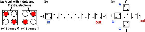
Figure 21.1 (a) QCA devices are typically comprised of four dots with two extra electrons; binary information is represented by charge configuration. (b) Electrostatic interactions propagate information from dot to dot in a QCA wire. (c) Electrostatic interactions also perform a majority voting function in a QCA majority gate
Alternatively, magnetic devices with nanometer feature sizes also are capable to move, process, and store information in a cellular automata-like architecture. Magnetic quantum-dot cellular automata (MQCA) devices – referred to here as Nanomagnet Logic (NML) per the latest naming convention from the ITRS [12] – will retain state without power, are radiation-hard, and are projected to dissipate less than 40 kT per switching event for a gate operation [13]. Experimentally, Cowburn performed the first room temperature experiments with QCA-like devices by showing that a magnetic soliton could propagate through a line of circular supermalloy discs [14]. Building on this work, researchers at the University of Notre Dame (ND) began to consider oval magnetic islands, which represent binary states due to magnetic shape anisotropy, and to explore potential approaches for clocking ensembles of NML devices – particularly focusing on how device shape could affect device to device coupling such that magnets in a circuit ensemble would settle into a logically correct state in response to a magnetic (clock) field and new inputs [15]. Additional research has since targeted – and experimentally demonstrated – the five essential “tenets” [16] that a digital device (i.e., NML) must satisfy: support for a functionally complete logic set (i.e., via majority logic gates [13] and/or 2-input AND/OR gates [17,18]), concatenability [13], nonlinear response characteristics [19], gain/fanout [20,21], and unidirectional dataflow [22]).
Given this technological state of the art, it is our belief that a magnetic implementation of the QCA device architecture (i.e., NML) represents the most viable path forward at the device level. For this reason, both our own research and this narrative considers the QCA architecture from the perspective of NML (although many of the ideas discussed here could be applied to the electrostatic QCA device architecture too).
Looking at the rest of this chapter, in Section 21.2, we will review the technological state of the art for different implementations of the NML device architecture. In Section 21.3, we address system-level architectures for NML assuming that the devices are used to implement “traditional” Boolean logic gates (adder designs and systolic arrays are discussed); Section 21.4 considers more unconventional NML-based information processing architectures (i.e., threshold logic, nonBoolean architectures, and cellular automata). Finally, in Section 21.5, we present our view on future prospects for the QCA device architecture – from a systems architecture perspective – and identify what we believe to be important and relevant future research directions.
21.2 Technology Background
21.2.1 An “In-Plane” Device Architecture
NML processes information via coupling between neighboring, nano-scale magnets. Most work with NML has focused on devices that couple in-plane (denoted iNML, see schematic in Figure 21.2a). (Recent work has also employed devices with out-of-plane, perpendicular magnetic anisotropy (PMA); this device architecture will be discussed in Section 21.2.2.).
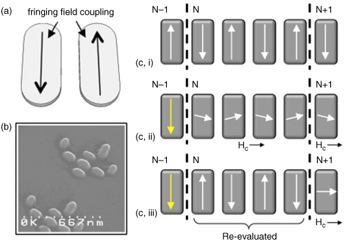
Figure 21.2 (a) iNML device schematic. (b) Scanning electron microscopy (SEM) of programmable majority gate. (c, i–iii) how an AF-line would be clocked
Since 2010, experimental progress (driven in part by our research group at the University of Notre Dame, as well as other groups at UC-Berkeley [23], VCU [24], South Florida [25], Minnesota (UMN) [26], and so on who are now studying NML) suggests that it is possible to move beyond isolated line and gate structures (e.g., the majority gate as shown in Figure 21.2b [19]), and toward more functional, circuit-level structures. Notably, fanout structures [20,21], a 1-bit full adder [27], and so on have been experimentally demonstrated and successfully re-evaluated with new inputs. Both field-coupled [28] and spin transfer torque (STT) [26,29,30] electrical inputs have been realized. For electrical output, multiple NML-magnetic tunnel junction hybrids [31–33] have been proposed and simulated.
Externally supplied switching energy is needed to re-evaluate (or clock) a magnet ensemble with new inputs. To modulate the energy barriers of iNML device ensembles “on-chip,” [34] proposed using hard axis directed magnetic fields from current driven wires. Ensembles of magnets could be grouped in clocking zones. Figure 21.2c illustrates the effects of the clocking field. From the initial state in Figure 21.2c,i, magnets in clocking zones N and N + 1 are put into a metastable logic state (i.e., along the hard/short axis) against the preferred shape anisotropy (Figure 21.2c,ii). If a driving neighbor (i.e., in zone N − 1) provides a y-directed biasing field, the driven magnet's magnetization rotates toward a preferred easy (long) axis. When the clock is removed, magnets should relax to a new, low energy ground state (Figure 21.2c,iii) in order. Clock energy could be amortized over hundreds of thousands of devices as a single clock line could control many parallel ensembles. Fringing fields from devices themselves also help with the transition to the 0/metastable state in Figure 21.2c,ii. As such, the magnitude of the required clock field (and current) need not be excessively high [34,35], and this approach to clocking could lead to performance “wins” at the application level [35–37]. Notably, proposals for line clock structures [34] were experimentally realized and used to flip the state of single magnets [38], as well as to re-evaluate lines and gates [22]. Moreover, recent experimental results [37,39,40] suggest that materials-based solutions could allow for further reductions in clock wire current.
iNML devices should also be amenable to voltage-controlled clocking, and multiferroics [41] and magnetostriction [24], have also been proposed as potential iNML clocks. Multiferroic materials (e.g., BFO) could allow for electric field control of magnetism [41]. uses multiferroic materials to demonstrate the switching of an in-plane ferromagnetic component (i.e., a nanomagnetic island). Also, [24] considers how the magnetization state of a multiferroic nanomagnet can be rotated via the coupling between a magnetostrictive layer and a piezoelectric layer. This work suggests that only 10 s of millivolts are needed to induce a rotation of 90° into a metastable state, and that stress-based clocking would lead to clock energy dissipation of just ∼200 kT per device.
If voltage-controlled clocking becomes feasible, it would almost certainly be the preferred approach for iNML clocking. When looking toward circuits and systems, potential advantages include reductions in clock energy [24], and more fine-grained control of an NML ensemble (useful architecturally as discussed in [42], and Section 21.3.1.4 of this document). That said, many of the architectural ideas discussed here are by in large amenable to current or voltage-controlled clocks – particularly as both clocking approaches place devices in metastable states for re-evaluation (a potential source of error that will be considered in Section 21.5).
21.2.2 An “Out-of-Plane” Device Architecture
A pNML device schematic is shown in Figure 21.3a. Thin PMA nanomagnets switch through nucleation and domain wall propagation [43,44]. Irradiation or ion milling could be used to define a “soft spot,” where a domain wall may nucleate. The nucleated wall subsequently propagates through the dot, fully reversing it. The coercivity of the magnet is determined by the coercivity of its highest-irradiated region. This reversal behavior is markedly different from in-plane permalloy nanomagnets, which remain nearly single-domain during switching and rotate coherently (through a 0/metastable state as described above).
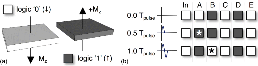
Figure 21.3 (a) Graphical representation of logic 0, 1 for pNML. (b) How information would move in an AF-ordered line (assuming the left edge of each magnet is FIB irradiated); * is used to show dataflow
Both computational [45] and experimental [46] results suggest that appropriately irradiated pNML structures can be controlled by a uniform, homogeneous, oscillating, global clock field. Consider the antiferromagnetically (AF) ordered line schematic in Figure 21.3b. Here, we (i) refer to the period of the sinusoidal, out-of-plane field as Tpulse with peak amplitude of Hpulse, and (ii) assume that dots are FIB irradiated on their left edges, so information will flow from left to right. After the first application of Hpulse (in the +z direction), the dot immediately adjacent to the flipped input will change state after 0.5 Tpulse. Switching occurs as Hpulse is of sufficient magnitude to eliminate parallel alignment in the dot pair at the input, but not of sufficiently high magnitude to alter the state of other dots in the line. (Again, irradiation location determines which dot will switch.) With successive applications of the time varying field, multiple bits of information can move through an AF-line segment simultaneously, and an inherent pipeline is created. Notably, majority gates [47], AF-lines [46], and full adders [48] comprised of multi-layered pNML devices have all been experimentally demonstrated.
When considering experimental realizations of “on-chip” clocks, large arrays of pNML devices could be controlled with on-chip inductor structures [49] that could be coupled with a capacitance in an LC oscillator – which opens the door to adiabatic energy recycling. pNML devices are also amenable to voltage-controlled clocking. Recent experiments suggest that it should be possible to change the easy axis of patterned CoFeB layers with PMA from out-of-plane to in-plane with modest voltages [50]. As such, a pNML device would transition through a metastable state with this clocking approach.
21.3 NML Circuit Design Based on Conventional, Boolean Logic Gates
21.3.1 Boolean Logic
Here, we consider the prospects for the NML device architecture when using NML devices to realize random, combinational logic blocks – for example, that might be used in a general-purpose microprocessor. We begin by discussing the pros and cons of the iNML and pNML device architectures (Sections 21.3.1.1–21.3.1.4), and conclude with an effort to quantitatively benchmark NML logic against CMOS equivalents. In Section 21.3.1, we will use an adder as a running case study.
21.3.1.1 Less Complex Signal Routing
When considering the layout of an iNML circuit, assuming a Cartesian grid, data will propagate through AF-ordered interconnect when moving in the ±x direction, and ferromagnetically (F)-ordered interconnect when moving in the ±y direction. As such, the x dimension (i.e., the width) of every device must essentially be fixed in order to allow for transitions between AF-ordered and F-ordered lines. Theoretically, this construct could be relaxed. As per Figure 21.4a, a line comprised of five devices that are each 60 nm wide, with 10 nm spacing between devices will have the same length as a line of seven devices that are 40 nm wide with 10 nm between devices. However, varying the size/aspect ratio of devices is difficult as: (i) clock field requirements can change significantly [51], (ii) very precise lithography would be required, (iii) variations to width are also limited in that we need to ensure devices remain single domain, and (iv) fringing fields from a smaller device may be insufficient to “drive” a larger device.
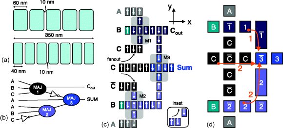
Figure 21.4 (a) With iNML, device size could be varied to create equal length line segments, but clocking requirements for the dots in each line can change significantly. (b) Majority gate-based full adder. (c) Schematic of iNML full adder. (d) Schematic of pNML full adder
Assuming iNML devices of constant size, transitions between F-ordered and AF-ordered interconnect can prove to be problematic when considering concatenated gate structures. As an example, consider a majority gate-based, one-bit full adder (see schematic in Figure 21.4b). Note that in this design, the carry input signal is fed to gates M1 and M3, while the complement of the carry signal is fed to gate M2. Also, the complement of M1 is required as an input to M3. Given the combination of AF- and F-ordered interconnect, obtaining the proper signal value at the desired gate input is difficult to achieve.
As a representative example, consider an iNML-based schematic of the 1-bit adder shown in Figure 21.4c. To better illustrate potential routing issues, we have made explicit copies of the A, B, and C inputs at each gate. If a single copy of the C input were to fan out to gates M1, M2, and M3, M1 and M2 would receive the wrong value. Using M2 as an example, the C input to gate M2 should have a negative y component of magnetization, but instead would have a positive y component of magnetization via F-ordered interconnect. While carry signal routing might be addressed by eliminating one magnet from the middle C input, the input to M3 would then be affected. One solution to this problem could be to create a staggered transition between AF- and F-ordered interconnect (see Figure 21.4c inset), and physical-level simulations suggest that such a structure may function properly, but this idea is unproven experimentally.
That said, this problem is much easier to address with pNML given that: (i) both x- and y-directed interconnect are AF-ordered, and (ii) that it is possible to vary the size of a given device. A potential pNML-based schematic of an adder appears in Figure 21.4d. By changing the size of the device that serves as the M1 and M2 input to M3, desired signal values can easily be routed to a given gate. While larger device sizes could impact the required length of Tpulse, ensembles with mixed dot sizes have been experimentally demonstrated [52], and thus no new constructs are required. Notably, magnets could be on the order of one micron long [53].
21.3.1.2 Data Races
Upon closer examination of Figure 21.4d, one might wonder whether or not “data races” could occur. Consider the input paths to M3. There is essentially just one (albeit larger) device between the output of gate M1 and the decision device in M3, there are two devices between the carry input and the decision magnet of M3, and there are two devices between the output of M2 and M3's decision magnet. (This does not even account for critical path differences given the initial evaluations of M1 and M2.) Thus, at issue is whether or not different signal arrival times will impact logical correctness.
For iNML, this is a potential concern. The success or failure of a gate is largely a function of clocking – for example, whether or not devices switch in a soliton-like fashion or devices switch in the presence of an applied clock field. With soliton-based switching, all devices in a circuit ensemble are placed into a 0°, metastable (MS) state – for example, by a clocking field. The external field is removed, and each device in the ensemble is expected to remain in a hard-axis-biased state until set by an appropriate neighbor. (While this is an unstable state of the system, dipole fields from neighboring magnets do help to preserve it [23].) All inputs to the ensemble are set, and easy axis directed fringing fields from said inputs cause neighboring devices to switch. Fringing fields from these devices then set the state of the next neighbor, and so on.
In [23], the authors noted that thermal noise could induce premature, random, and unwanted switching. To combat this problem [23], suggested fabricating magnetic islands with a magnetocrystalline biaxial anisotropy – that is, such that U(θ) becomes Ku cos2(θ) + ¼K1 sin2(2θ), where K1 is the biaxial anisotropy constant. The biaxial anisotropy term introduces a local minimum in the energy landscape of an individual magnetic island at 0° – which should further promote the hard axis stability of the ensemble. Given the effects of thermal noise at T = 300 K [23], reports that a line of hard-axis biased devices with a biaxial term remained in a 0°/MS state until a device was set by an appropriate neighbor, when a device without the biaxial term did not.
In [54], Spedalieri et al. extended the work of [23] and considered the switching behavior of a suite of majority gates with biaxial anisotropy. The clocking scheme assumed in [54] was similar to the approach used in [23] (and explained above). Notably, assuming gates comprised of 30 × 15 × 6 nm magnets, the gate error rate can exceed 15%. The most common errors observed were: (i) premature switching in randomized islands due to thermal noise and (ii) gates where devices essentially remained hard-axis biased (due to a biaxial constant/biaxial anisotropy that was too large).
It was also shown that sufficiently strong coupling fields in the case of pNML [68] or sufficiently small clocking zones in the case of iNML [69] reduce error rates to an acceptable level, where circuit-level solutions can be used for eliminating errors.
Alternatively, magnets can also be driven to a new, logically correct state before a clocking field is removed. [55] reports gate simulations where inputs do not arrive at a decision magnet simultaneously, but the gate still functions correctly. The clock field is applied until all signals arrive at the compute magnet, and it has time to respond. (The clock field prevents a decision magnet from relaxing prematurely.) While this approach to switching may prevent race conditions, it will also: (i) result in an increase in clock energy and (ii) make successive devices in a group weaker drivers, eventually limiting the width of a clock line.
As with signal routing, managing potential data races can be much easier with FIB-irradiated pNML. To illustrate, consider the majority gate (with some initial state) shown in Figure 21.5. As before, we will assume an out-of-plane, sinusoidal field as shown in Figure 21.3b. Now, assume that the top and middle inputs to this gate change state (see Figure 21.5b). The time evolution of the gate is shown in Figure 21.5c–j. Even though the output of the gate changes state after the new, middle input arrives (Figure 21.5f), it changes back to the logically correct state after the new, top input arrives (Figure 21.5i). As the middle input is unchanged, no metastabilities in the second input arm appear, and the compute device is allowed to react to all inputs.
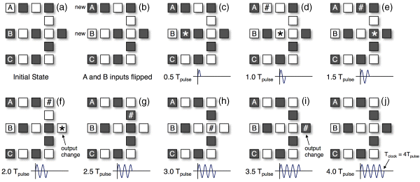
Figure 21.5 Time evolution of an pNML majority gate when subjected to a sinusoidal, out-of-plane field; data propagation from A and B inputs is illustrated with # and * respectively
Finally, consider an NML ensemble where multiple levels of logic are connected together. Using the above gate as an example, if we define Tclock to be NTpulse (Figure 21.5j), where N is defined by the longest critical path through a bit slice, we can synchronize the application of new inputs in successive bit slices to ensure that a well-timed circuit (and logically correct output) is achieved.
21.3.1.3 Pipeline Depth
For iNML, a multi-phase clock is required to define dataflow directionality through a magnet ensemble (Figure 21.2c). However, controlling an iNML ensemble with multiple clock lines – for example, an extended AF-line segment like that shown in Figure 21.6a – results in an inherent pipeline, which will improve circuit throughput. More specifically, every time data propagates completely through a clock group, a new input can begin to traverse the same group. Essentially, a new value can be written into or read out of our AF-line/shift register every time the last wire cycles through all ϕ phases (where ϕ would equal three for a three-phase clock). The magnets overlaid on top of N wires (where N is the number of clock phases) represent a bit of information (see Figure 21.6a).
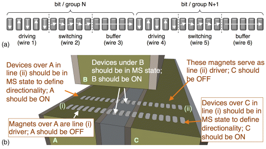
Figure 21.6 (a) Bit definition in an iNML AF-line (three-phase clock). (b) Why bi-directional dataflow is difficult to achieve with line-based, three-phase clock
Assuming a line clock, the number of magnets per pipe stage will ultimately be limited by the width of a given line (see Figure 21.6b). Practically, this cannot be arbitrarily small as narrow clock wires will: (i) have a much higher resistance which will adversely affect clock energy and (ii) making very narrow, clad lines (i.e., less than 100 nm wide) with good field confinement will obviously become prohibitive. This is not to say that a bit of information could not traverse multiple gates within a given group, but only one bit could be stored per AF-ordered line that traverses a given group (Figure 21.6a).
We reiterate that other approaches for clocking iNML are also being studied. As noted earlier, potential advantages to electric field-based clocking include additional energy reductions, and more fine-grained control of an ensemble – which could lead to deeper pipelines. (It should be noted that a potential disadvantage of the aforementioned clocks is that every device may need to be contacted individually, which would increase fabrication complexity.) That said, in a pNML ensemble, pipe depth could be completely independent of clock feature size, and devices do not need to be contacted individually (i.e., assuming domain wall switching modes). Regarding fabrication and throughput, this would obviously be advantageous.
21.3.1.4 Achieving Bi-directional Dataflow
Information processing hardware for countless applications requires feedback – which implicitly suggests that bi-directional dataflow is required. Assuming a line clock, with iNML, three clock wires (as shown in Figure 21.6b) cannot facilitate dataflow in multiple directions (e.g., in parallel, AF-ordered lines). Assuming we want data to flow from left to right in line (i) and from right to left in line (ii), the two AF-ordered lines would require different excitation patterns. For example, for line (i), wires A, B, and C should be OFF, ON, and ON respectively, while for line (ii), wires A, B, and C should be ON, ON, and OFF respectively. Thus, for a line clock, bi-directional dataflow must be accomplished at the granularity of the clock structures themselves. However, for pNML, directionality can be achieved simply by changing the position of FIB irradiation. Similarly, with voltage-controlled clocking, bidirectional dataflow could be achieved in a fine-grained manner for both iNML and pNML.
21.3.1.5 Benchmarking
Here, we briefly discuss energy and performance metrics for iNML and pNML adder designs. We begin by considering recent results from the NRI's architectural-level benchmarking efforts led by Nikonov and Young – where multiple devices were evaluated assuming a common set of fabrication parameters and circuit-level benchmarks (see [56] for more detail). Note that as only the iNML device architecture was rigorously vetted through the NRI, only results that project the energy, delay, and throughput of iNML current and voltage-controlled 32-bit adders are discussed below. (The adder design used in [56] is based on the design in Figure 21.4c.) That said, we do conclude this subsection by briefly comparing and contrasting the iNML and pNML adder designs in Figure 21.4c and d.
We particularly wish to highlight the impact of inherent pipelining on an iNML-based adder's performance/energy/throughput. Notably, the NRI's benchmarking analysis “[does] not incorporate any pipelining in [these] calculations, even though some logic technologies are not constrained by power dissipation may produce higher computational throughput by pipelining.” As per the discussion above, NML circuits could (and should) be inherently pipelined with no overhead. Thus, as per Figure 21.7a, computations in an adder could overlap. If we conservatively assume that 10 adds are active simultaneously, as per Figure 21.7b and c, (generated via the code associated with [56]) the energy–delay products of iNML adders improve and become competitive with low power CMOS. Furthermore, standby power effects, intangibles regarding operating environments, and so on could represent added benefits. Moreover, as per Figure 21.7d, the throughput per unit area of an iNML adder (quantified as peta-integer operations per second, per square centimeter) moves into the most desirable area of the plot.
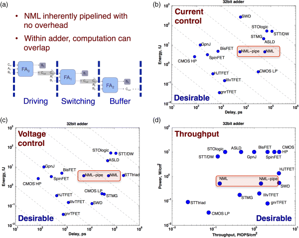
Figure 21.7 (a) Inherent pipelining in ripple carry adder. (b) NRI projections for 32-bit adder assuming current-controlled switching of spin-based devices – the impact of inherent pipelining on performance/energy of the iNML device architecture is noted. (c) NRI projections for 32-bit adder assuming (magnetostictive) voltage controlled switching of spin-based devices – the impact of inherent pipelining on performance/energy of the iNML device architecture is noted. (d) NRI projections for throughput assuming magnetostrictive, voltage-controlled switching of spin-based devices – the impact of inherent pipelining on performance/energy of the iNML device architecture is noted. (PIOPS/cm2 refers to the number of peta-integer operations per cm2)
Finally, the pNML device architecture could offer additional advantages. When comparing the adder design schematics in Figure 21.4c (iNML) and Figure 21.4d (pNML) the number of devices in the critical path in the pNML design is 6 less than the iNML design (8 vs. 14). Furthermore, even if iNML devices with 20 × 30 nm footprints were employed, the area of the one-bit design would be essentially the same as a pNML design comprised of devices with 50 × 50 nm footprints and 50 × 100 nm footprints (i.e., 0.133 μm2 for iNML vs. 0.136 μm2 for pNML). (Differences can largely be attributed to ease in signal routing.)
21.3.2 Systolic Arrays
Here, we consider alternative, system-level architectures (e.g., nonVon Neumann architectures) that might employ NML devices to perform Boolean logic functions. Of particular interest are architectural approaches that can exploit deeply pipelined logic, and avoid large-scale interconnect.
21.3.2.1 Architecture Overview
We anticipate that NML-based hardware will be used to implement systolic architectures [57] that would in turn process information in the aforementioned application spaces. The nearest neighbor interactions and inherently pipelined logic associated with NML map extremely well to systolic architectures developed in the late 1970s and early 1980s [57]. In a systolic architecture, data flows from a computer's memory, through many (and often identical) processing elements, before returning to memory. Additional processing is done on some subset of data by each processing element. As such, this can significantly reduce the need for global signal broadcasts. This should allow us to minimize NML's drawbacks (nearest neighbor dataflow and higher latency devices when compared to CMOS) and exploit its more desirable features (inherently pipelined logic with no overhead).
As one example, consider the convolution problem where, given a sequence of weights w1, w2,…wk and the input sequence x1, x2,…xk, the resulting sequence yi = w1xi + w2xi+1 + wkxi+k−1 is calculated. Also, if the multiplication and addition operations in the convolution expression above are transformed to Boolean XOR and AND operations, the convolution operation would be transformed to a pattern matching operation. In either instance, streams of data would flow from left to right while a cumulative output would flow from right to left. (And as noted in Section 21.3.1.4, this can be achieved for iNML via voltage-controlled clocking and for pNML with either a global clock or a voltage-controlled clock.)
Moreover, future information processing workloads will be required to perform information processing tasks that have natural systolic solutions. Systolic solutions exist for many problems including filtering, polynomial evaluation, discrete Fourier transforms, matrix arithmetic and other nonnumeric applications involving graphing algorithms and data structures. Below, we will present a more thorough case study of pattern matching (PM) hardware – which is needed at the application-level for data mining, genomics, intrusion detection, and so on.
21.3.2.2 Toward NML Implementations of Systolic Architectures
The fundamental processing element (PE) in a systolic PM circuit appears in Figure 21.8a. Individual bits of a data stream serve as one input to an XNOR gate. The other input to the XNOR is a bit (bi) of a pattern of interest. (This bit of information could be stored directly at the gate in a nonvolatile, NML device. We are investigating the use of spin transfer torque (STT) to program the b bits.) If the bits match, the output of the XNOR gate is a logic 1; otherwise a logic 0 results. This output then becomes one input to the AND gate – the output of which captures the global history of multiple, concatenated PEs. If at any point the output of an XNOR gate is a 0, the accumulated global history is set to 0, which suggests that there is no match in input stream bits xm…xm+n (see Figure 21.8b).
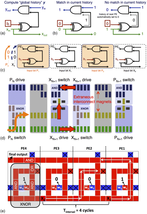
Figure 21.8 (a) Logic gates in a systolic PM PE. (b) How PE functions assuming match/no match in incoming input stream. (c) Concatenated PEs to examine a four-bit pattern; while x inputs must be staggered by one PE to ensure global history bits and new x inputs arrive at next PE simultaneously, input streams (e.g., P0-to-n, X0-to-n) can be interleaved to achieve full hardware usage. (d) Schematic of potential iNML-based systolic array that: (i) assumes voltage-controlled clocking (shading color denotes common clock phases) and (ii) the existence of a two-input XOR gate for simplicity (see [17] for possible realizations of this gate). (e) Concatenated pNML PEs – to reconcile pNML timing requirements, need to stagger x inputs by 4Tpulse if no interleaving
More specifically, when a computation commences, bits from the input data stream (x0…xn) flow through the sequence of PEs (i.e., from left to right, as per Figure 21.8). When the first input bit (x0) arrives at the rightmost PE (PE0 in Figure 21.8c), initialization is complete, and streaming data analysis can begin. Thus, bit x0 would be compared to bit w0 via an XNOR operation, and the output of this gate would then be ANDed with the input signal yin – initialized to logic “1.” This “global history” is then shifted to an adjacent (left) PE (e.g., PE1 in Figure 21.8c) such that we can consider the next bit of the input stream. When the shifted global history reaches the leftmost PE (PE3 in Figure 21.8c), a match is detected if the initial logic “1” has been preserved.
That said, some architectural-level timing constraints must also be satisfied. For instance, bits of the input stream must be “spaced” two PEs apart to ensure that global history bits and streaming input data meet at the proper time. (Note the position of x1 in Figure 21.8c). This will degrade circuit throughput. However, two different input streams could be interleaved within the systolic array – assuming that one would want to search for the same pattern in each. Interleaved dataflow (e.g., p1, x1, p0, x0 as noted in Figure 21.8c) would allow for full hardware usage and the highest possible throughput.
21.3.2.3 An iNML Implementation
A schematic representation of an iNML realization of the PEs depicted in Figure 21.8a/Figure 21.8c appears in Figure 21.8d. Here, voltage clocking is assumed (as per Figure 21.6b, fine-grained bi-directional dataflow cannot be easily achieved with a line clock). The color of the underlying shading denotes clock phase, and arrows/labels denote how interleaved data streams would flow through the systolic array. (Note that for simplicity, this schematic assumes the existence of a two-input XNOR gate – which could be possible per [17]). By eliminating extraneous interconnect magnets (see labeled devices in Figure 21.8d) the critical path through a given PE could be reduced.
21.3.2.4 A pNML Implementation
A pNML-based design for the PM systolic array appears in Figure 21.8e. To perform the required AND function, a majority voting gate is essentially transformed to an AND gate by hard-coding one input to logic “0.” Similarly, the XNOR gate is realized by performing the operation A“B + AB.” Again, majority gates are transformed to AND and OR gates by hard-coding inputs to logic “0”s and logic ‘1”s respectively. As reported in [49,58], the functionality of this design has been verified by micromagnetic simulation.1
By taking advantage of the ability to selectively size pNML devices,2 it is possible to balance the critical paths through PE1 and PE0. This allows us to reconcile the architectural-level timing requirements of the bidirectional systolic array with those of the pNML clock – for example, to ensure that the output of PE0 is coordinated with the evaluation of the XNOR gate in PE1. Thus, the output of the XNOR in PE1, and the output (from the AND gate) in PE0 should arrive at the AND gate in PE1 simultaneously. This allows the input data stream to move through the systolic array uninterrupted to avoid stalls and maximize throughput. As highlighted in Figure 21.8e, the interval between x inputs is regular and equal to 4Tpulse. This suggests that after the pipeline/systolic array is filled (i.e., the first bit of the input stream reaches PE0), a new response/match check will exit the systolic array every 4Tpulse time units (if data is not interleaved), and every 2Tpulse time units (if data is interleaved). Simulations of this particular design suggest that the circuit functioned properly when subjected to an out-of-plane field where Hpulse was approximately ±70 mT, and Tpulse was 15 ns.
21.3.2.5 Benchmarking
While a detailed discussion is beyond the scope of this document we do note that projected area–energy–delay projects could be 50–130× better than CMOS functional equivalents (even when inherent pipelining is introduced into CMOS designs) [59]. Similarly, the energy associated with pNML-based designs could be one or two orders of magnitude better than CMOS functional equivalents at iso-performance [49,60].
21.4 Alternative Circuit Design Techniques and Architectures
Here, we consider more “unconventional’ approaches for processing information with the NML device architecture. Specifically, approaches for, and the impact of using NML to realize threshold logic gates (Section 21.4.1), nonBoolean information processing hardware (Section 21.4.2), and cellular automata (Section 21.4.3) are all discussed. Again, comparisons to CMOS equivalents are made whenever appropriate/possible.
21.4.1 Threshold Logic
We believe that devices with PMA (i.e., pNML) could be especially well-suited for realizing threshold logic circuits. As an example, we consider how an adder comprised of multiple layers of pNML-based devices might fare given the context of the most recent NRI benchmarking effort.
The design (Figure 21.9) is based on the two majority gate threshold adder from [61]. The carry output (Cout) can be determined simply by performing the majority voting function M(A, B, Cin) that is native to NML [13]. The sum output can then be realized by a five-input majority voter: ![]() . With the in-plane device architecture, the single domain limit necessitates that device footprint be relatively small which limits fan-in. pNML devices can not only be larger (increasing fan-in), but can also couple in multiple dimensions. Note that in Figure 21.9, the AF-coupling between the A, B, and C inputs and the Cout target would result in the generation of
. With the in-plane device architecture, the single domain limit necessitates that device footprint be relatively small which limits fan-in. pNML devices can not only be larger (increasing fan-in), but can also couple in multiple dimensions. Note that in Figure 21.9, the AF-coupling between the A, B, and C inputs and the Cout target would result in the generation of ![]() . Additionally, by placing the Sum target above A, B, Cin, and
. Additionally, by placing the Sum target above A, B, Cin, and ![]() , the correct signal values will be fed to Sum.3 (The Sum target is sized such that the fringing field magnitude from Cout is two times that of A, B, or Cin.) As such, a full adder can be realized with just five devices. If we assume that F = 15 nm (as is done in the most recent NRI benchmarking), with this approach, a 32-bit adder could be ∼45× smaller than an iNML-based design and ∼145× smaller than a CMOS design. Moreover, as the carry out signal and sum signals could be calculated simultaneously (see Figure 21.10b—generated via the code associated with [56]), a single, 32-bit add could be completed in the time required for 33 magnet switching events (a 900% reduction compare to iNML). as per Figure 21.10a, this could make the power-constrained throughput of pNML-based hardware highly competitive with respect to other NRI technologies (without even considering any additional benefits from inherent pipelining associated with NML).
, the correct signal values will be fed to Sum.3 (The Sum target is sized such that the fringing field magnitude from Cout is two times that of A, B, or Cin.) As such, a full adder can be realized with just five devices. If we assume that F = 15 nm (as is done in the most recent NRI benchmarking), with this approach, a 32-bit adder could be ∼45× smaller than an iNML-based design and ∼145× smaller than a CMOS design. Moreover, as the carry out signal and sum signals could be calculated simultaneously (see Figure 21.10b—generated via the code associated with [56]), a single, 32-bit add could be completed in the time required for 33 magnet switching events (a 900% reduction compare to iNML). as per Figure 21.10a, this could make the power-constrained throughput of pNML-based hardware highly competitive with respect to other NRI technologies (without even considering any additional benefits from inherent pipelining associated with NML).
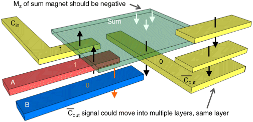
Figure 21.9 Schematic of integrated adder cell using pNML. (Assuming “0” maps to ↓, and “1” maps to ↑, the magnetization state for input combination A = 1, B = 0, Cin = 1 is shown.) Note that the Cout magnet (with a complemented value) could move a signal up in the vertical direction to another level, or within the same plane
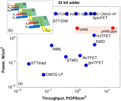
Figure 21.10 (a) Multi-layer pNML circuits offer the promise of high computational throughput (in the context of existing NRI benchmarking work). Note that power projections are based on existing NRI data for magnetostrictive switching. PIOPS/cm2 refers to the number of peta-integer operations per cm2. (b) Schematic showing concatenated bits. In a pipelined circuit, a new result could be completed every two clock cycles after the pipeline is filled
21.4.2 NonBoolean Computing
We also believe that NML devices could be used to create nonBoolean information processing systems. As an example, we summarize work presented in [60] that considers an arrangement of pNML devices that could be used for image edge detection.4
To begin, consider the arrangements of pNML devices shown in Figure 21.11a. Red boxes represent devices that are magnetized up (+Mz). Later, blue boxes will represent devices that are magnetized down (−Mz). Thus, to make an analogy to a black and white image, one could equate a −Mz magnetization state of an input device to a white pixel, and a +Mz magnetization state to a black pixel.) Input devices could presumably be set via STT [62], and are indicated by green boxes. While pNML devices are assumed, we assume that no dots are FIB irradiated. Therefore, in Figure 21.11a, we might assume that all pNML devices (in both the “interconnect” as well as the inputs) were initially magnetized such that their z-component of magnetization was positive (i.e., by an external field, voltage-based clock, and/or STT.). Additionally, this suggests that a 3 × 3 black square is encoded by this magnet arrangement.
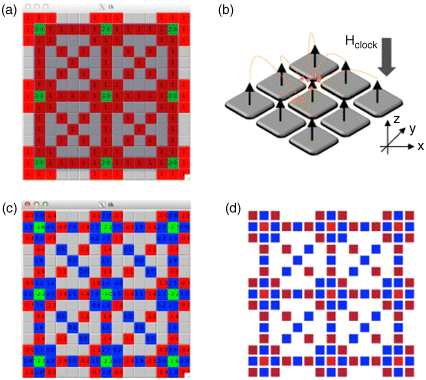
Figure 21.11 (a) Arrangement of pNML devices for edge detection. (b) Fringing fields and a clock field influence which pNML device would switch first – here, a middle device experiences the highest downward directed field (−Hz). (c) Intermediate state of system shown in Figure 21.11a assuming downward directed field. (d) Micromagnetic simulations (at 0 K) very similar to projected states in Figure 21.11c. (Minor differences most likely due to direction of nominal x, y-directed biasing fields)
Now, assume that we subject this system to an out-of-plane field that is directionally opposite to the magnetization state of “interconnect” magnets (per Figure 21.11a, a negative Hz field would be applied), and that gradually increases in magnitude. One would expect pNML devices that have more neighbors with a +z component of magnetization to switch first as fringing fields from neighboring devices – also directed in the −z direction – influence switching as well. (As an example, looking at Figure 21.11b, the middle device should switch first as it influenced by both the applied external field as well as neighboring fringing fields.)
In initial studies, we assumed that a given magnet is influenced by devices that are two “squares” away – that is, devices that are closer to a given device will have more influence over it than those that are farther away. (Practically speaking, the pNML design space is large, and the influence of particular device could be “tuned” by changing dot size, material, spacing between dots, irradiating dots, or combinations thereof.) We also assume that the state of the input dots does not change during the switching process – which could be achieved by varying device size, limited FIB irradiation, or combinations thereof. Thus, given different assumptions regarding neighbor to neighbor influence, we calculated how susceptible a given device is to switching when subjected to an out-of-plane field.
If we assume: (i) that the influence of a given magnet falls of as 1/r2, (ii) the arrangement of magnets (with the initial state) shown in Figure 21.11a, and (iii) that this magnet ensemble is subjected to a field that is directed in the opposite direction to the initial magnetization state of the devices, the final state of the system is predicted to be similar to that shown in Figure 21.11c.5
Note that the number of cells that surround the center input devi`ce that were initially magnetized down (opposite to the direction of the applied field) is lower than the number of cells that surround devices that are now magnetized up. However, the number of devices that surround the input devices on the “edge” of the 3 × 3 black square is lower (i.e., for the center pixel, 6 of the 8 surrounding devices have changed state, while for the edge pixels, only 4 or 5 of the surrounding devices have changed state). If one could measure the resistance of the input and its surrounding cells, one could detect the edges in a black and white image with: (i) a short field pulse per the discussion above and (ii) resistance measurements.6 Therefore, even though NML devices have longer switching latencies than a CMOS transistor, an edge detection operation could be accomplished with just a single field pulse and simultaneous reads. The devices in the system “evolve” in parallel.
Notably, micromagnetic simulations suggest that the magnet ensemble described above will evolve almost as predicted (see Figure 21.11d). (Minor differences between Figure 21.11c and Figure 21.11d most likely result from the direction of the nominal x- and y-directed biasing fields that initiate a torque on a given pNML device.) That said, micromagnetic simulations were performed at 0 K, and multiple devices can switch simultaneously as appropriate (e.g., due to the influence of equally weighted neighbors in this environment.) However, we will ultimately need to consider how thermal noise [12] impacts ordered switching. For example, if one cell switches first, it may impact another cell that should switch at the same time, which could impact final system state.
21.4.3 Cellular Automata
Cellular Automata (CA) is a classic and early example of computationally universal nonBoolean computing and ancestor of many modern cellular architectures (such as CNNs). It displays two highly desirable architectural properties of a realizable nano-scale computing system: high-level of parallelism, and nearest neighbor interconnections [63].
In the first step of a CA computation, each computing units (cells) of a CA have to initialized to a certain (possibly digital) value – the initialization pattern can be looked as an input image. Once initialized, the cell's state evolves in discrete time according to a logical rule and the result of the computation is read out after a number of computing steps elapsed. This computing scheme clearly lends itself to a natural realization in pNML architectures.
As a case study for a two-dimensional pNML-based cellular automata, we implemented an image filtering algorithm as described in [64]. Noise of a black and white image can be reduced by: (i) assigning a cell for each pixel of the image, (ii) in every CA iteration, each cell assumes the pixel value of the majority of its neighbors and itself, and (iii) the iteration is repeated for several (5–15) steps until the noise disappears but the image still retains most of its useful information. In these scheme each cell requires an external input/output (for initialization and read-out) and interconnections to the neighboring cells (to determine their majority). The results of the filtering similar to the ones obtainable by a standard Gaussian filter.
A pNML implementation we designed is shown in Figure 21.12. The design does not require any wire crossings and it is entirely tileable, that is, an arbitrary number of cells can be placed and the output (input) of each cell can directly contact the input (output) of its neighbors. Details of the design and simulation results are given in [65].
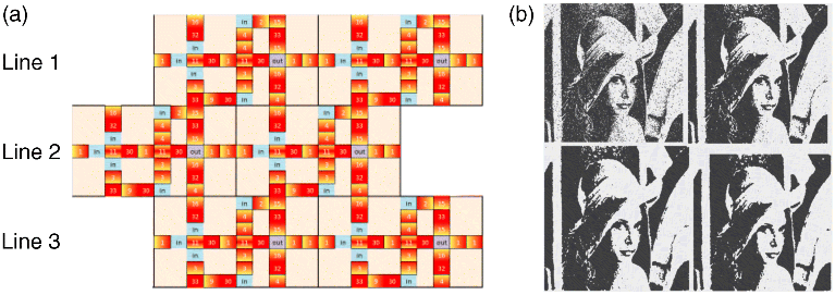
Figure 21.12 (a) Six cells of a noise-filtering CA, realized from pNML dots. The lighter side of the dots denotes their irradiated side. Note that even-index and odd-index lines obey slightly different rules and they are shifted with respect to each other, so the design is tillable. (b) Image processing results using the modified CA rule: the original image and the processed image is shown after four, eight and 12 iterations, respectively
In order to arrive to this simple design, we slightly changed the used CA rule of [64] and a slightly different rule is applied to even and odd-numbered rows. For even-numbered rows the updated value of the state variable of cell i, j is:
and for rows with odd indices:
where i, j are the column and row indices of the cell.
These cell rules ignore one neighbor (out of the four) and take into account another one with a double weight. We found that although it is a different CA rule from the one described in [64], it performs the filtering operation equally well: as it is shown in the images of Figure 21.12b. The noisy original image clears up after four, eight, and 12 iterations. The overhead of inputting and reading out the image amortized over these number of iteration steps.
Signal race conditions may cause undesired operation of this CA (or any other CA operation): depending on the data being processed some cells may pass data to neighboring cells “too early” and the computing units of the CA fall out of synchrony. To prevent this, the designs needs “transfer dots,” that enable the flow of magnetic information only after each eighth clocking cycles, where all cell outputs are ready. These transfer dots are labeled as “in” in Figure 21.12a.
21.5 Retrospective, Future Challenges, and Future Research Directions
Here, we briefly review what we believe are important issues and paths to pursue in order for NML/QCA-like devices to become a viable information processing technology.
21.5.1 Retrospective: Experimental Progress to Date
When compared to other emerging information processing technologies, we believe that there has been significant progress with both iNML and pNML on the experimental front. For iNML, fanout structures [21], a one-bit full adder [27], and so on have been experimentally demonstrated and successfully re-evaluated with new inputs. Both field-coupled [28,66] and spin transfer torque (STT) [26,29,30] electrical inputs have been realized. For electrical output, multiple iNML-magnetic tunnel junction hybrids [33] have been proposed and simulated.
Field-based, CMOS compatible line clock structures have been used to simultaneously switch the states of multiple magnetic islands [38], as well as to re-evaluate iNML lines and gates with new inputs [22]. Additionally, recent experiments have considered materials-based solutions to further reduce field/energy requirements for line clock structures. Notably, results from [37,39] suggest that the component energy metrics could be further reduced by as much as 16×. Alternative clocking mechanisms – for example, via multiferroics [41], magnetostriction [24], or the Spin Hall Effect [67] – might also be paths to further reductions in clock energy.
Experimental results suggest that appropriately irradiated pNML structures (to define dataflow directionality) can be controlled by a uniform, homogeneous, oscillating, global clock field [46]. Majority gates [47], AF-lines [46], multi-plane signal crossings [68], and full adders [48,69] have all been experimentally demonstrated with this clocking approach. Field coupled inputs have also been demonstrated [70].
Looking to chip-level implementations, large arrays of pNML devices could be controlled with on-chip inductor structures [49] that could be coupled with a capacitance in an LC oscillator – which opens the door to adiabatic energy recycling. Devices with PMA are also amenable to voltage-controlled clocking [50].
That said, for both device architectures, challenges still remain – particularly with respect to efficient interconnect, reliable device switching, and fault tolerant architectures.
21.5.2 Challenge 1: Efficient Interconnect
One challenge associated with processing information using devices that communicate via fringing fields is interconnect. Signal routing and signal propagation times can be adversely affected. Devices with PMA can help to alleviate the aforementioned issues. With respect to signal routing, the large single-domain size in pNML enables the use of long (several micrometer) domain walls for information transfer. Moreover, per [63] CoPt domain walls can cross above/below one other, and conducing stripes can cross a 30 nm vertical “step” without unwanted pinning. Moreover, simulations suggest that by creating a nucleation center where two stripes cross, the interaction can be switched on, and one of the walls can stop or pass the other wall depending on their relative orientation. (Conditional passing of domain walls may even be used to realize PLAs.) The benefits of NML/domain-wall logic hybrids are threefold: (i) the footprint of domain wall-based devices is reduced and electrical components are necessary only at the inputs and outputs, (ii) interconnect complexity and delay of dot-based interconnections in NML is also reduced, and (iii) more reliable signal transmission may ensue.
Regarding signal propagation times (as well as signal routing), consider an array multiplier – where bits of data word A must be distributed to processing elements in each column of the multiplier, and the bits of data word B must be distributed to processing elements (PE) in each row of the multiplier. If one were to move this information to individual PEs via AF-lines, both signal routing and communication delay would be adversely affected. However, domain wall motion in magnetic stripes above and below NML processing elements could be used to preprogram PEs with the A and B input bits required – vastly simplifying design layout. (The work presented in [71] could be considered to be a preliminary, experimental proof of concept.)
21.5.3 Challenge 2: Error Tolerance
Any circuit and/or architecture comprised of NML devices must ultimately be tolerant to fabrication variations. Consider an iNML device with a symmetric, rounded-rectangle shape. A given device will be in the highest energy state if magnetized along its hard axis with no applied field (see Figure 21.12). However, lower energy states are equivalent and occur at ±90 °. [With no external stimulus to keep such a device in a hard axis-biased state, thermal noise, minor fabrication variations, etc. should determine whether or not it relaxes such that its y-component of magnetization is positive (↑) or negative (↓).] By changing a magnet's geometry, its energy landscape can change as well. More specifically, if the edge of a magnet becomes “slanted,” the highest-energy state does not occur when a device is magnetized along its (geometrically) hard axis. Rather, if biased along its geometrically hard axis, a device is already on one side of the potential barrier and should always relax such that the sign of the y-component of magnetization (i.e., its binary state) is always the same – see Figure 21.13. If devices are sufficiently large, we can exploit the aforementioned energy barrier shift to realize nonmajority gate, two-input AND/OR logic [55]. However, as device sizes scale, the effects of minor fabrication variations on device switching behavior can become more pronounced. If energy barrier shifts like those described above occur, a stuck at fault can ensue.
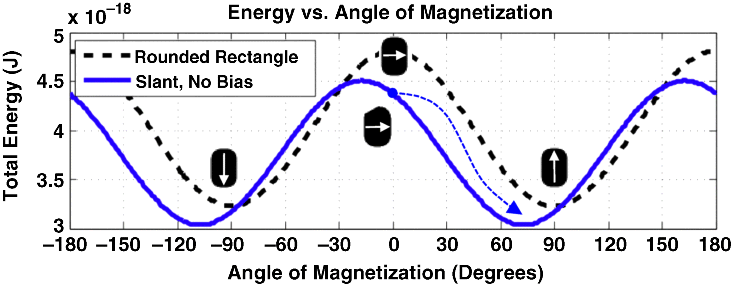
Figure 21.13 Total energy curves for slant-edge and rounded rectangle magnet – device with slanted edge already on one side of barrier in 0° state
In pNML, switching field distributions (SFD; from defects formed during layer growth) can impact operation. The width of SFD strongly depends on layer deposition conditions, postgrowth annealing and the applied FIB dose. Thermally induced SFD also have a strong effect. Initial studies show that coupling fields are sufficiently strong to ensure device operation in the presence of SFD [72].
21.5.4 Paths Forward
While NML circuits show benefits over CMOS-based logic, a “killer application” has yet to emerge. We envision that NML circuits may become especially useful in applications, which require close integration of data storage and processing functions. The combination of dense, nonvolatile, possibly three-dimensional storage capabilities of coupled nanomagnet arrays with processing capabilities (such as the systolic pattern matching or image processing) may serve as hardware for future intelligent storage devices.
A challenge with scaled NML is unwanted bit flips that can occur during the switching process due to thermal noise, lithographic variation, and so on. At the device level, improved device to device couplings [73,74] and devices with biaxial anisotropy [23] have been suggested as possible mechanisms to improve the reliability of an NML-based computation. However, even magnet ensembles that employ devices with biaxial anisotropy can be error prone [54]. Thus, fault tolerant architectures should be studied and developed. Of initial interest are stochastic computer architectures where the value of a signal is interpreted as a probability regardless of normal or faulty conditions. Stochastic computation is naturally fault tolerant since a small number of bit flips only result in small deviations from the desired value. While computation time could increase as the precision of stochastic values increases, given the inherently pipelined, streaming dataflow associated with NML, more efficient implementation of stochastic computation architectures should be possible with NML devices (e.g., as one of the main drawbacks of stochastic computation is the rapid growth of computation time with respect to precision).
Notes
References
- 1. Lent, C.S., Tougaw, P.D., Porod, W., and Bernstein, G.H. (1993) Quantum cellular automata. Nanotechnology, 4, 49–57.
- 2. Orlov, A.O., Amlani, I., Bernstein, G.H. et al. (1997) Realization of a functional cell for quantum-dot cellular automata. Science, 277, 928–930.
- 3. Amlani, I., Orlov, A.O., Toth, G. et al. (1999) Digital logic gate using quantum-dot cellular automata. Science, 284, 289–291.
- 4. Orlov, A.O., Kummamuru, R.K., Ramasubramaniam, R. et al. (2001) Experimental demonstration of a latch in clocked Quantum-dot cellular automata. Applied Physics Letters, 78, 1625–1627.
- 5. Kummamuru, R.V., Timler, J., Toth, G. et al. (2002) Power gain in a quantum-dot cellular automata latch. Applied Physics Letters, 81, 1332–1334.
- 6. Yadavalli, K.K., Orlov, A.O., Timler, J.P. et al. (2007) Fanout gate in quantum-dot cellular automata. Nanotechnology, 18, 375401.
- 7. Jiao, J., Long, G.J., Grandjean, F. et al. (2003) Building blocks for the molecular expression of quantum cellular automata: Isolation and characterization of a covalently bonded square array of two ferrocenium and two ferrocene complexes. Journal of the American Chemical Society, 125, 7522–7523.
- 8. Lent, C.S. and Tougaw, P.D. (1997) A device architecture for computing with quantum dots. Proceedings of the IEEE, 84, 541–557.
- 9. Qi, H., Sharma, S., Li, Z. et al. (2003) Molecular Quantum Cellular Automata cells: electric field driven switching of a silicon surface bound array of vertically oriented two-dot molecular quantum cellular automata. Journal of the American Chemical Society, 125, 15250–15259.
- 10. Haider, M.B., Pitters, J.L., DiLabio, G.A. et al. (2009) Controlled coupling and occupation of silicon atomic quantum dots at room temperature. Physical Review Letters, 102, 046805.
- 11. Mitic, M., Cassidy, M.C., Petersson, K.D. et al. (2006) Demonstration of a silicon-based quantum cellular automata cell. Applied Physics Letters, 89, 013503-3.
- 12. ITRS (2012) International Technology Roadmap for Semiconductors. Available www.itrs.net.
- 13. Imre, A., Csaba, G., Ji, L. et al. (2006) Majority logic gate for magnetic quantum-dot cellular automata. Science, 311, 205–208.
- 14. Cowburn, R.P. and Welland, M.E. (2000) Room temperature magnetic quantum cellular automata. Science, 287, 1466–1468.
- 15. Bernstein, G.H., Imre, A., Metlushko, V. et al. (2005) Magnetic QCA systems. Microelectronics Journal, 36, 619–624.
- 16. Waser, R. (2003) Nanoelectronics and information technology: Advanced electronic materials and novel devices, Wiley-VCH, Weinheim.
- 17. Kurtz, S., Varga, E., Niemier, M. et al. (2011) Two input, non-majority magnetic logic gates: experimental demonstration and future prospects. Journal of Physics: Condensed Matter, 23, 053202.
- 18. Varga, E., Siddiq, M., Niemier, M.T. et al. (2010) Experimental Demonstration of Non-Majority, Nanomagnet Logic Gates, Device Research Conference, pp. 87–88.
- 19. Varga, E., Niemier, M.T., Bernstein, G.H. et al. (June 22 2009) Non-volatile and Reprogrammable MQCA-based Majority Gates, Device Research Conference, pp. 1–2.
- 20. Varga, E., Liu, S., Niemier, M.T. et al. (2010) Experimental Demonstration of Fanout for Nanomagnet Logic, Device Research Conference, Notre Dame, IN, pp. 95–96.
- 21. Varga, E., Orlov, A., Niemier, M.T. et al. (2010) Experimental demonstration of fanout for nanomagnetic logic. IEEE Transactions on Nanotechnology, 9, 668–670.
- 22. Alam, M.T., Kurtz, S., Siddiq, M.J. et al. (2012) On-chip clocking of nanomagnet logic lines and gates. IEEE Transactions on Nanotechnology, 11, 273–286.
- 23. Carlton, D.B., Emley, N.C., Tuchfeld, E., and Bokor, J. (2008) Simulation Studies of Nanomagnet-Based Logic Architecture. Nano Letters, 8, 4173–4178.
- 24. Salehi, F.M., Roy, K., Atulasimha, J., and Bandyopadhyay, S. (2011) Magnetization dynamics, Bennett clocking and associated energy dissipation in multiferroic logic. Nanotechnology, 22, 155201.
- 25. Pulecio, J.F. and Bhanja, S. (2010) Magnetic cellular automata coplanar cross wire systems. Journal of APhys., 107, 034308.
- 26. Lyle, A., Harms, J., Klein, T. et al. (2012) Spin transfer torque programming dipole coupled nanomagnet arrays. Applied Physics Letters, 100, 012402-3.
- 27. Varga, E., Niemier, M.T., Csaba, G. et al. (2013) Experimental Realization of a Nanomagnet Full Adder Using Slanted-Edge Input Magnets, INTERMAG/MMM, Chicago, IL.
- 28. Siddiq, M.A.J., Niemier, M.T., Bernstein, G.H. et al. (2013) A Field Coupled Electrical Input for Nanomagnet Logic, accepted for publication in IEEE Transactions on Nanotechnology.
- 29. Lyle, A., Harms, J., Klein, T. et al. (2011) Integration of spintronic interface for nanomagnetic arrays. AIP Advances, 1, 042177 11.
- 30. Lyle, A., Klemm, A., Harms, J. et al. (2011) Probing dipole coupled nanomagnets using magnetoresistance read. Journal of Applied Physics, 98, 092502.
- 31. Liu, S., Hu, X.S., Nahas, J. et al. (2011) Design and optimization of magnetic-electrical interfaces for NML circuit output, Design Automation Conference, Work-in-progress session.
- 32. Liu, S., Hu, X.S., Nahas, J.J. et al. (2011) Magnetic-electrical interface for nanomagnet logic. IEEE Transactions on Nanotechnology, 10, 757–763.
- 33. Liu, S., Hu, X.S., Niemier, M.T. et al. (2013) A design space exploration of the magnetic-electrical interfaces for nanomagnet logic. IEEE Transactions on Nanotechnology, 12, 203–214.
- 34. Niemier, M.T., Hu, X.S., Alam, M. et al. (2007) Clocking Structures and Power Analysis for Nanomagnet-Based Logic Devices, International Symposium on Low Power Elec. and Design (ISLPED), Portland, OR, pp. 26–31.
- 35. Dingler, A., Niemier, M.T., Hu, X.S., and Lent, E. (2011) Performance and Energy Impact on Locally Controlled NML Circuits. ACM Journal on Emerging Technologies in Computing, 7, 1–24.
- 36. Dingler, A., Niemier, M., Hu, X.S. et al. (2009) System-Level Energy and Performance Projections for Nanomagnet-based Logic, 2009 IEEE/ACM International Symposium on Nanoscale Architectures (NANOARCH), pp. 21–26.
- 37. Li, P., Csaba, G., Sankar, V.K. et al. (2012) Power Reduction in Nanomagnet Logic Clocking through High Permeability Dielectrics, Device Research Conference, State College, Pennsylvania, pp. 129–130.
- 38. Alam, M.T., Siddiq, M.J., Bernstein, G.H. et al. (2010) On-chip clocking for nanomagnet logic devices. IEEE Transactions on Nanotechnology, 9, 348–351.
- 39. Li, P., Csaba, G., Sankar, V.K. et al. (2013) Paths to Clock Power Reduction via High Permeability Dielectrics for Nanomagnet Logic Circuits, Joint MMM/Intermag Conference, Chicago, IL.
- 40. Li, P., Sankar, V.K., Csaba, G. et al. (2012) Magnetic properties of enhanced permeability dielectrics for NML circuts. IEEE Transactions on Magnetics, 48, 3292–3295.
- 41. Chu, Y.H., Martin, L.W., Holcomb, M.B. et al. (2008) Electric-field control of local ferromagnetism using a magnetoelectric multiferroic. Nature Materials, 7, 478–482.
- 42. Crocker, M., Hu, X.S., and Niemier, M. (2010) Design and Comparison of NML Systolic Architectures, 2010 IEEE/ACM International Symposium on Nanoscale Architectures (NANOARCH), pp. 29–34.
- 43. Becherer, M., Kiermaier, J., Breitkreutz, S. et al. (2010) On-chip Extraordinary Hall-effect sensors for characterization of nanomagnetic logic devices. Solid State Electronics, 54, 1027–1032.
- 44. Shaw, J.M., Russek, S.E., Thomson, T. et al. (2008) Reversal mechanisms in perpendicularly magnetized nanostructures. Physical Review B, 78, 024414.
- 45. Ju, X., Wartenburg, S., Rezgani, J. et al. (2012) Nanomagnet logic from partially irradiated Co/Pt nanomagnets. IEEE Transactions on Nanotechnology, 11, 97–104.
- 46. Eichwald, I., Bartel, A., Kiermaier, J. et al. (2012) Nanomagnet Logic: error-free directed signal transmission by an inverter chain. IEEE Transactions on Magnetics, 48, 4332–4335.
- 47. Breitkreutz, S., Kiermaier, J., Eichwald, I. et al. (2012) Majority gate for nanomagnetic logic with perpendicular magentic anisotropy. IEEE Transactions on Magnetics, 48, 4336–4339.
- 48. Breitkreutz, S., Kiermaier, J., Eichwald, I. et al. (2013) Experimental Demonstration of a 1-bit Full Adder in Perpendicular Nanomagnetic Logic, to appear in IEEE Transactions on Magnetics, vol. 49.
- 49. Ju, X., Niemier, M., Becherer, M. et al. (2013) Systolic pattern matching hardware with out-of-plane nanomagnet logic devices. IEEE Transactions on Nanotechnology, 12, 399–407.
- 50. Wang, W.-G., Li, M., Hageman, S., and Chien, C.L. (2012) Electric-field-assisted switching in magnetic tunnel junctions. Nature Materials, 11, 64–68 01//print.
- 51. Dingler, A., Kurtz, S., Niemier, M. et al. (2012) Making Non-Volatile Nanomagnet Logic Non-Volatile, Design Automation Conference (DAC), pp. 476–485.
- 52. Becherer, M., Csaba, G., Emling, R. et al. (2009) Field-coupled Nanomagnets for Interconnect-Free Nonvolatile Computing, International Solid-State Circuits Conference, ISSCC, pp. 474–475.
- 53. Hellwig, O., Berger, A., Kortright, J.B., and Fullerton, E.E. (2007) Domain structure and magnetization reversal of antiferromagnetically coupled perpendicular anisotropy films. Journal of Magnetism and Magnetic Materials, 319, 13–55.
- 54. Spedalieri, F.M., Jacob, A.P., Nikonov, D.E., and Roychowdhury, V.P. (2011) Performance of magnetic quantum cellular automata and limitations due to thermal noise. IEEE Transactions on Nanotechnology, 10, 537–546.
- 55. Niemier, M.T., Bernstein, G.H., Csaba, G. et al. (2011) Nanomagnet logic: Progress toward system-level integration. Journal of Physics: Condensed Matter, 23, 493202.
- 56. Nikonov, D. E. and Young, I. A. (2013) Overview of Beyond-CMOS Devices and a Uniform Methodology for Their Benchmarking, Proceedings of the IEEE, 101(12), 2498–2533.
- 57. Kung, H.T. (1982) Why systolic architectures? Computer, 15, 37–46.
- 58. Ju, X., Niemier, M.T., Becherer, M. et al. (2012) Design of a Systolic Pattern Matcher for Nanomagnet Logic, IWCE 2012 (International Workshop on Computational Electronics, University of Wisconsin-Madison, May 2012).
- 59. Bernstein, G., Csaba, G., Hu, X.S. et al. (2012) Nanomagnet Logic, NRI Annual Review, Gaithersburg, Maryland.
- 60. Niemier, M., Ju, X., Becherer, M. et al. (2012) Boolean and Non-Boolean Architectures for Out-of-Plane Nanomagnet Logic, Procedings of the International Workshop on Cellular Nanoscale Networks and their Applications, August 29–31 2012, pp. 1–6.
- 61. Lageweg, C., Cotofana, S., and Vassiliadis, S. (2002) A full adder implementation using SET based linear threshold gates, Electronics, Circuits and Systems, 2002. 9th International Conference on, vol. 2. pp. 665–668.
- 62. Mangin, S., Ravelosona, D., Katine, J.A. et al. (2006) Current-induced magnetization reversal in nanopillars with perpendicular anisotropy. Nature Materials, 5, 210–215.
- 63. Toffoli, T. and Margolus, N. (1987) Cellular Automata Machines: A New Environment for Modeling, MIT press.
- 64. Popovici, A. and Popovici, D. (2002) Cellular Automata in Image Processing, Fifteenth International Symposium on Mathematical Theory of Networks and Systems.
- 65. Haughan, K. (2013) Cellular Automata Designs for Out of Plane Nanomagnetic Logic, to be submitted for IEEE Conference on Nanotechnology.
- 66. Siddiq, M.A., Niemier, M., Csaba, G. et al. (2013). Demonstration of Field Coupled Input Scheme on Line of Nanomagnets, accepted in IEEE Transactions on Magnetics.
- 67. Bhowmik, D., Long, Y., and Salahuddin, S. (2012) Possible route to low current, high speed, dynamic switching in a perpendicular anisotropy CoFeB-MgO junction using Spin Hall Effect of Ta, Electron Devices Meeting (IEDM), 2012 IEEE International. pp. 29.7.1–29.7.4.
- 68. Eichwald, I., Wu, J., Kiermaier, J. et al. (2013) Towards a Signal Crossing in double-layer Nanomagnetic Logic, to appear in IEEE Transactions on Magnetics, vol. 49.
- 69. Breitkreutz, S., Eichwald, I., Kiermaier, J. et al. (2013) 1-Bit Full Adder in Perpendicular Nanomagnet Logic using a Novel 5-Input Majority Gate, accepted at the Joint European Magnetic Symposium (JEMS), Rhodos, Greece, August 25–30 2013.
- 70. Kiermaier, J., Breitkreutz, S., Csaba, G. et al. (2012) Electrical input structures for nanomagnetic logic devices. Journal of Applied Physics, 111, 07E341 3.
- 71. Varga, E., Csaba, G., Bernstein, G.H., and Porod, W. (2012) Domain-wall assisted switching of single-domain nanomagnets. Magnetics, IEEE Transactions on, 48, 3563–3566.
- 72. Breitkreutz, S., Kiermaier, J., Ju, X. et al. (2011) Nanomagnetic Logic: Demonstration of Directed Signal Flow for Field-coupled Computing Devices, ESSDERC Helsinki, Finnland.
- 73. Breitkreutz, S., Kiermaier, J., Yilmaz, C. et al. (2011) Nanomagnetic logic: compact modeling of field-coupled computing devices for system investigations. Journal of Computational Electronics, 10, 352–359.
- 74. Csaba, G. and Porod, W. (2010) Behavior of Nanomagnet Logic in the presence of thermal noise, Computational Electronics (IWCE), 2010 14th International Workshop on, pp. 1–4.