
11
Molecular Transistors
Mark A. Reed1, Hyunwook Song2, and Takhee Lee3
1Departments of Electrical Engineering and Applied Physics, Yale University, USA
2Department of Applied Physics, Kyung Hee University, Korea
3Department of Physics, Seoul National University, Korea
11.1 Introduction
Since Aviram and Ratner initially proposed a molecular rectifier in 1974 to predict the feasibility of constructing a functional molecular device using single molecules as the active elements [1], the field of molecular electronics has attracted significant interest over the past few decades [2–9]. The concept of making a functional device based on the properties inherent in a single molecule offers fascinating possibilities due to the potentially diverse electronic functions of the component molecules that can be tailored by chemical design and synthesis. Within the past few years, a wide range of characteristic functions illustrated by single molecules has been reported, including diodes [10–12], transistors [13–16], switches [17–21], and memory [21–23]. Single molecules provide ideal systems to investigate charge transport on the molecular scale, which is a subject of intense current interest for both practical applications and achieving a fundamental understanding of novel physical phenomena that take place at this length scale. This chapter focuses primarily on experimental aspects of devices that consist of one or very few molecules contacted between external electrodes. In particular, we concentrate on the characterization and manipulation of charge transport in this regime.
11.2 Experimental Approaches
11.2.1 Fabrication Methods
The fabrication of single-molecule electronic devices is a very challenging task. Conventional lithography is still unable to deliver resolution at the molecular scale, and it is beyond the capability of traditional microfabrication technologies. Nevertheless, a broad range of groups have devised a number of sophisticated experimental techniques. For an extended discussion, we refer the interested reader to the excellent reviews on various experimental testbeds of molecular electronic devices by Chen et al. [24], Akkerman et al. [6], McCreery et al. [8], and Li et al. [25] The common concept in all of these methods is the ability to form nanometer-sized gap (nanogap) electrodes. Individual molecules can occasionally bridge a gap between electrodes, thus creating reliable molecular junctions that allow charge transport measurements through constituent single molecules.
A common approach adopted to create molecular-scale electrode gaps is called a “break junction.” Break junctions can be categorized into two types: mechanically controllable break junctions and electromigrated break junctions. Mechanically controllable break junctions (MCBJs) were introduced by Moreland et al. [26] and Muller et al. [27] This technique consists of a lithographically defined, metallic free-suspended bridge or a notched wire above a gap etched in an insulating (polymer or oxide) layer, fixed on the top of a bendable substrate [28–39]. The bendable substrate is most often made from a phosphor–bronze sheet owing to its superior mechanical deformation properties. This substrate is put in a three-point bending geometry, where it can be bent by moving a piezo-controlled pushing rod, as illustrated in Figure 11.1. As the substrate is bent, the metallic wire is elongated until finally the metallic constriction breaks and two fresh electrode surfaces are created. The molecules can be assembled between the separate gap electrodes by different methods. For example, one can break the electrodes while molecules are present either in solution [32] or in the gas phase [37] or by adding a solution with the desired molecules after the breakage of the metallic wire [38,39]. The first example of MCBJs to make molecular junctions was illustrated by Reed et al. (see Figure 11.1b and c) in 1997 [32]. In this study, a gold wire was covered with a self-assembled monolayer (SAM) of 1,4-benzenedithiol (BDT), which is able to bind to two gold electrodes through thiol groups. The gold wire was subsequently elongated in the molecular solution until breakage. Once the wire was broken, the solvent was evaporated and the wires were brought together until the onset of a conductance value. With the proper control experiments (which were performed identically but without the molecules), the measured conductance value could be ascribed to a small number (ideally one) of BDT molecules bridging the gap. One of the main advantages of MCBJs is that the contact size can be continuously adjusted under the precise control of a piezoelectric component without polluting the junction. Furthermore, the ability to repeat back and forth bending of the flexible substrates allows statistics to be obtained using a large number of measurements of the target molecule [30,31,37]. Although the exact local configuration of the junctions is unknown, it is evident from theoretical studies that the exact shape, configuration, and mechanical stress of the metal-molecule contacts are very important in influencing the result of experiments on single molecules [40–43].
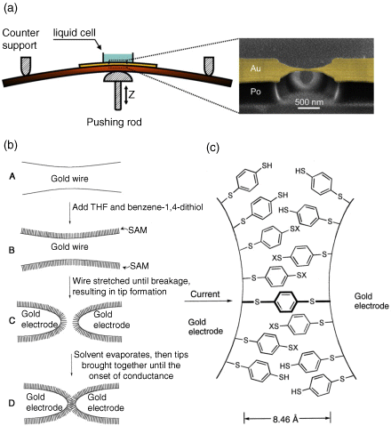
Figure 11.1 (a) Schematics of the MCBJ principle with a liquid cell and a SEM image of the central part of the microfabricated Au junction. Po is a polymer insulating layer. Reproduced with permission from [28]. Copyright 2008 American Chemical Society. (b) Schematic of the measurement process. Step A: The gold wire of the break junction before breaking and tip formation. Step B: After addition of 1,4-benzenedithiol, SAMs form on the gold wire surfaces. Step C: Mechanical breakage of the wire in solution produces two opposing gold contacts that are SAM-covered. Step D: After the solvent is evaporated, the gold contacts are slowly moved together until the onset of conductance is achieved. Steps C and D (without solution) can be repeated numerous times to test for reproducibility. Reproduced with permission from [32]. Copyright 1997 Science. (c) Schematic of a 1,4-benzenedithiol SAM between proximal gold electrodes formed in an MCBJ. The thiolate is normally H-terminated after deposition; end groups denoted as X can be either H or Au, with the Au potentially arising from a previous contact/retraction event. These molecules remain nearly perpendicular to the Au surface, making other molecular orientations unlikely. Reproduced with permission from [32]. Copyright 1997 Science
Electromigrated break junctions (EBJs) were first developed by Park et al. in 1999 [44]. The controlled passage of a large density current or the application of a large direct current voltage to a continuous thin metal wire predefined by electron-beam lithography causes the electromigration of metal atoms and the eventual breakage of the metal wire (Figure 11.2a). If performed properly, a separate electrode pair with distances of approximately 1–2 nm can be created so that the target molecule can subsequently bridge the gap between the broken electrodes. To incorporate the molecules into EBJs, two different approaches can be taken. One approach is to either deposit the molecules onto the electrode surface, after which the breaking process proceeds, or to first break and then assemble the molecules into the separate electrodes. Because a gate electrode can be readily fabricated on the substrate before the breaking process is performed by electromigration, the EBJs are especially advantageous in making three-terminal device configurations (see Figure 11.2a) [14,16,45]. In contrast to MCBJs, the nanogap junctions formed by electromigration cannot make a large repetitive collection of measurements with the same junction. Thus, a large number of devices must be fabricated to examine the statistical behavior of the electromigration breaking process [44,46,47]. Moreover, the technique must be used with care. The local heating of the junction during electromigration can increase the temperature, resulting in large gaps, the destruction of the molecules, and the formation of gold islands inside the gap [48]. Unintentional metal debris in the gap interferes with the insertion of the molecules of interest and can mask the intrinsic molecular signals [49–52]. Careful correlation of spectroscopies can be used to eliminate the presence of metal islands. Recently, a few groups prepared electromigrated nanogaps on free-standing transparent SiNx membranes to permit the use of transmission electron microscopy (TEM) to image the nanogap formation in situ (Figure 11.2b) [53,54].
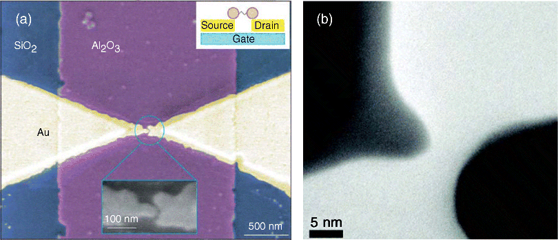
Figure 11.2 (a) SEM image of the metallic electrodes fabricated by electron beam lithography and the electromigrated break junction technique. The image shows two gold electrodes separated by 1 nm above an aluminum pad, which is covered with an 3-nm layer of aluminum oxide. The whole structure is defined on a silicon wafer. The central regions correspond to a gold bridge with a thickness of 15 nm and a minimum lateral size of 100 nm. The outer regions represent portions of the gold electrodes with a thickness of 100 nm. Reproduced with permission from [45]. Copyright 2002 Nature Publishing Group. (b) TEM images of a typical electromigrated nanogap on SiNx membrane. Reproduced with permission from [53]. Copyright American Chemical Society
Scanning tunneling microscopy (STM) and conducting-probe atomic force microscopy (CP-AFM) has also been widely used to measure the charge transport properties of a very small number of molecules (from several tens of molecules to a single molecule). The strength of STM lies in its combination of high-resolution imaging and spatially resolved electrical spectroscopy (so-called scanning tunneling spectroscopy, STS), providing the local density of states with atomic spatial resolution [55–57]. In general, the electrical contact is accomplished through the air gap (or vacuum tunneling gap, in ultrahigh vacuum STM) between the molecule or the molecular monolayer and the STM tip, which leads to considerable difficulty in evaluating the true conductance of single molecules. A significant improvement was demonstrated by Xu et al. [58], who measured the conductance of a single molecule by repeatedly forming several thousands of metal–molecule–metal junctions. This technique is referred to as a STM-controlled break junction (STM-BJ). In STM-BJs, molecular junctions are repeatedly and quickly formed by moving the STM tip into and out of contact with a metal electrode surface in a solution containing the molecules of interest. Single or a few molecules, bearing two anchoring groups at their ends, can bridge the gap formed when moving the tip back from the surface (Figure 11.3a). Because of the large number of measurements possible, this technique provides robust statistical analysis of the conductance data, and histograms of the conductance evolution during breaking show evidence of the formation of molecular junctions [58–68].
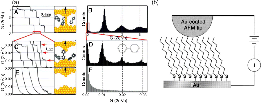
Figure 11.3 (a) Graph A: Conductance of a gold contact formed between a gold STM tip and a gold substrate decreases in quantum steps near multiples of G0 (= 2e2/h) as the tip is pulled away from the substrate. Graph B: Corresponding conductance histogram constructed from 1000 conductance curves as shown in graph A shows well-defined peaks near 1 G0, 2 G0, and 3 G0 due to conductance quantization. Graph C: When the contact shown in graph A is completely broken, corresponding to the collapse of the last quantum step, a new series of conductance steps appears if molecules such as 4,4′ bipyridine are present in the solution. These steps are due to the formation of the stable molecular junction between the tip and the substrate electrodes. Graph D: Conductance histogram obtained from 1000 measurements as shown in graph C shows peaks near 1 ×, 2 ×, and 3 × 0.01 G0 that are ascribed to one, two, and three molecules, respectively. Graphs E and F: In the absence of molecules, no such steps or peaks are observed within the same conductance range. Reproduced with permission from [58]. Copyright 2003 Science. (b) Formation of a molecular junction by contacting an alkanethiol self-assembled monolayer with an Au-coated AFM tip. Reproduced with permission from [69]. Copyright 2000 American Chemical Society
In CP-AFM [69–76], the metal-coated tip, acting as the top electrode, is gently brought into direct contact with the molecules on a conducting substrate, acting as the bottom electrode (this process is monitored by the feedback loop of the AFM apparatus) while an external circuit is used to measure the current–voltage characteristics (Figure 11.3b). This procedure eliminates the current reduction caused by the extra tunneling gap in the STM setup [67,74–76]. However, the conducting probe tip of the CP-AFM coated with a metallic layer is significantly larger than an atomically sharp STM tip [69,75]. This difference produces a higher uncertainty in the number of molecules measured. Furthermore, one needs to consider the roughness and morphology of the bottom electrode substrate to estimate the number of molecules under investigation. The critical requirement for CP-AFM measurements is the very sensitive control of the tip-loading force to avoid applying excessive pressure to the molecules [77]. Excessive pressure may modify the molecular conformation and thus its electronic properties. On the other hand, the ability to apply a controlled mechanical pressure to a molecule to change its conformation can be a powerful tool to investigate the relationship between conformation and charge transport in molecular junctions [72,73,78].
A number of other approaches have been tried to create two electrodes with a molecular-sized gap for electronic transport experiments on molecular junctions. For example, Morpurgo et al. [79] proposed electrochemical deposition in which the inter-electrode distance can be tuned on the atomic scale in an aqueous solution by depositing (or removing) atoms at a low rate. Another method to control the inter-electrode distance on the molecular scale was reported by Kubatkin et al. [15] Using a shadow mask technique and evaporation at variable angles in ultrahigh vacuum (UHV) conditions, they obtained well-defined molecular devices under clean conditions and at low temperatures. An alternative method to overcome the mismatch between the resolution of lithographic methods and the molecular size was described by Dadosh et al. [80] using gold nanoparticles with a typical diameter of 10 nm. The molecules can be attached to the gold particles by thiol bonds such that they form particle–molecule–particle dumbbells from solution. Recently, single-walled carbon nanotubes (SWNT) have been used as electrodes separated by a nanogap (less than 10 nm) [81]. The nanogap electrodes can be obtained by a precise oxidation cutting of the SWNT, and the two facing SWNT ends that are terminated by carboxylic acids are covalently bridged by the molecules of interest functionalized with amine groups at both ends. These functionalized contacts can be used to fabricate devices with a variety of molecules, acting as pH sensors [81], photogated switches [82], and DNA hybridization sensors [83]. Very recently, Bjørnholm et al. [84] showed a new method for the direct synthesis and growth of end to end linked gold nanorods using gold nanoparticle seeds with a dithiol-functionalized poly(ethylene glycol) (SH-PEG-SH) linker. This method results in a nanogap with a size of 1–2 nm between two gold rods, which suggests the possibility of fabricating nanogap electrodes incorporating a single molecule or several molecules by bottom-up chemical assembly.
11.2.2 Electronic Transport Fundamentals
A full understanding of the transport properties of a molecular junction represents a key step towards the realization of single-molecule electronic devices and requires detailed microscopic characterization of the active region of the junction. Indeed, a hurdle in most single-molecule electronic devices is the unambiguous demonstration that the charge transport occurs only through a single molecule of interest. For these reasons, the analysis of the transport properties of the molecular junction attracts much attention in the field, and a variety of experimental techniques have been established in recent years.
The charge transport mechanism of a molecular junction can be revealed by the characteristic temperature[85–87] and length dependences [87–89]. Therefore, measurements of temperature- and length-variable transport for the molecular junction are necessary to examine the charge transport mechanism. In particular, two distinct transport mechanisms have been extensively discussed in the literature [2,5,6,8,85–90]: coherent transport via tunneling or superexchange and incoherent thermally activated hopping. Coherent tunneling or superexchange dominates through relatively short molecules and the conductance value (G) decreases exponentially as the molecular length increases, according to Equation 11.1:
where d is the molecular length, and β is the tunneling decay coefficient (varying between 0.7–0.9 Å−1 for alkyl chains and 0.2–0.5 Å−1 for π-conjugated molecules). In addition to the exponential decay of the conductance with molecular length, this coherent tunneling process is characterized by temperature-independent transport. On the other hand, incoherent hopping is known to be responsible for charge transport along long-conjugated molecular wires, and the conductance follows an Arrhenius relation given by:
where kB is the Boltzmann constant, T is the temperature, and Ea represents the hopping activation energy. The incoherent charge hopping is also characterized by a weak length-dependent transport that results in conductance that scales linearly with the inverse of the molecular length.
From Reference [87], Figure 11.4a shows a representative temperature-variable current–voltage [I(V)] of 1,8-octanedithiol bridging the Au nanogap electrodes broken by electromigration as described in the previous section. The I(V) curves were measured between 4.2 and 90 K, and no temperature dependence was observed [87]. The temperature-independent I(V) characteristic is a clear manifestation of coherent tunneling transport and eliminates many other potential mechanisms. In this study [87], the conductance of five different alkanedithiols having between eight (DC8) and 12 (DC12) carbon atoms was also measured to examine the length-dependent conductance (Figure 11.4b). In accordance with Equation 11.1, a semilog plot of the conductance versus the molecular length was linear. From the linear fit (the solid line across data points) in Figure 11.4b, the β value was found to be 0.88 (= 0.71 Å−1) per carbon atom, assuming a through-bond tunneling [87]. This β value is in good agreement with the previously reported values of alkyl chains in literature [70,86]. Thus far, a consistent picture has emerged for the coherent tunneling mechanism of saturated alkyl chains and short-length conjugated molecules [86,91,92]. The coherent tunneling transport can be reasonably expected when the Fermi energy of the electrode lies within the large energy gap between the highest occupied molecular orbital (HOMO) and the lowest unoccupied molecular orbital (LUMO) of the short molecules. Collectively, the correct exponential decrease of conductance upon a molecular length increase, the temperature-independent I(V) characteristics, and the agreement with decay coefficients all point to the formation of a valid molecular junction.
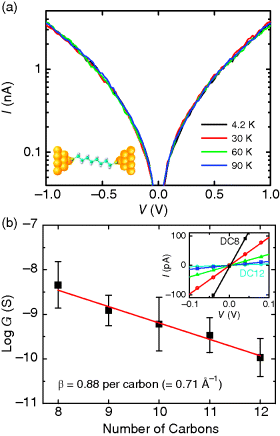
Figure 11.4 (a) Semilog plot of temperature-variable I(V) characteristics for Au–1,8-octanedithiol–Au junctions at selected temperatures (4.2, 30, 60, and 90 K). (b) Semilog plot of the conductance versus the number of carbon atoms for five different length alkanedithiol nanogap junctions. The decay coefficient (β) can be determined from the linear fit (the solid line), yielding a β value of 0.88 (= 0.71 Å−1) per carbon atom. Inset shows length-dependent I(V) curves in the low-bias linear regime, where a conductance value is obtained from linear fits to the data. Reproduced with permission from [87]. Copyright American Chemical Society
Conjugated molecules made of repeating units with modulated molecular length are ideal for understanding charge transport mechanisms because these molecular systems permit the investigation of not only coherent tunneling and incoherent hopping but also the transition between two distinct transport mechanisms by systematically changing the molecular length [88,90]. This transition from tunneling to hopping was observed by Frisbie and colleagues [88], who synthesized oligophenyleneimine (OPI) molecules of various lengths (ranging from 1.5 to 7.3 nm) bonded to Au through a thiolate linkage. The OPI molecular wires were grown on the Au substrate by stepwise imination with alternating addition of benzene-1,4-dicarboxaldehyde and benzene-1,4-diamine, as shown in Figure 11.5a. The transport characteristics of the OPI wires were then measured using CP-AFM. In the semilog plot of resistance versus molecular length (Figure 11.5b), a clear transition of the length dependence of resistance was observed near 4 nm (OPI 5), indicating that the transport mechanism is different in short (OPI 1 to 4) and long (OPI 6 to 10) wires. In the short wires, the linear fit in Figure 11.5b indicates that the data are well-described by Equation 11.1 for coherent nonresonant tunneling. The β value is found to be 3.0 nm−1, which is within the range of β values of typical conjugated molecules [93]. For long OPI wires, a much flatter resistance versus molecular length relation (β ∼ 0.9 nm−1) was shown. The extremely small β value suggests that the principal transport mechanism is incoherent hopping [88]. A plot of resistance versus molecular length for long OPI wires is linear (see Figure 11.5b, inset), which is consistent with hopping as described above and indicates that Equation 11.1 does not apply for the long wires [88]. The change in transport mechanism apparent in the length-dependent measurements was verified by the temperature dependence. Figure 11.5c shows that the resistance for OPI 4 is independent of temperature from 246 to 333 K, as expected for tunneling. On the other hand, both OPI 6 and OPI 10 display the strongly thermally activated transport that is characteristic of hopping [88]. The activation energies determined from the slopes of the data were identical at 0.28 eV for both OPI 6 and OPI 10 [93].
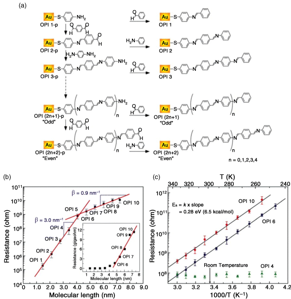
Figure 11.5 (a) Molecular structure and synthetic route to oligophenyleneimine wire precursors (OPI-p) and OPI monolayers on gold substrates. (b) Measurements of molecular wire resistance with CP-AFM. A gold-coated tip was brought into contact with an OPI monolayer on a gold substrate. The I-V traces were obtained over ±1.5 V for OPI 3 to 10 and ±1.0 V for OPI 1 and 2 at a load of 2 nN on the tip contact. Semilog plot of resistance versus molecular length for the gold/wire/gold junctions. Each data point is the average differential resistance obtained from 10 I(V) traces in the range −0.3 to +0.3 V. Error bars, 1 SD. Straight lines are linear fits to the data according to Eq. Eq. (11.1). (Inset) A linear plot of resistance versus molecular length, demonstrating linear scaling of resistance with length for the long OPI wires. (c) Arrhenius plot for OPI 4, OPI 6, and OPI 10. Each data point is the average differential resistance obtained at six different locations on samples in the range −0.2 to +0.2 V. Error bars, 1 SD. Straight lines are linear fits to the data. Reproduced with permission from [88]. Science
Hines et al. [90] also reported results that support a transition between tunneling and hopping in series of conjugated single-molecule junctions by carrying out both length- and temperature-dependent measurements of conductance using a STM-BJ method. These results provide experimental support for a theoretically predicted transition from tunneling for short molecules to thermally activated hopping for longer molecules [94,95].
Poot et al. [96] showed the temperature dependence of gated three-terminal molecular junctions containing sulfur end-functionalized tercyclohexylidenes. At low temperatures, they found temperature-independent transport, and at temperatures above 150 K, the current increased exponentially with increasing temperature (Figure 11.6). Over the entire temperature range (10–300 K) and for different gate voltages, a simple model [97] of transport through a single level well-described the experimental results, which indicates that the temperature dependence arises from the Fermi distribution in the leads [96].
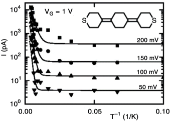
Figure 11.6 Current as a function of inverse temperature of the sulfur end-functionalized tercyclohexylidene molecule (see the inset) for four different source–drain voltages (50, 100, 150, and 200 mV), plotted for gate voltage of 1.0 V. Reproduced with permission from [96]. Copyright 2000 American Chemical Society
11.2.3 Molecular Junction Spectroscopies
A critical question is the identity of the molecules that inhabit the active region of the junction. Inelastic electron tunneling spectroscopy (IETS), an all-electronic spectroscopy due to localized molecular vibrational modes, was discovered in 1966 by Jaklevic and Lambe [98]. This pioneering work clearly showed the ability to detect the vibrational features of molecules buried in the interface of a metal–insulator–metal (MIM) device. To explain the principles of IETS (see also Reference [99]), Figure 11.7 shows the energy-band diagrams of a tunnel junction and the corresponding I(V), dI/dV, and d2I/dV2 plots. When a negative bias (small with respect to the tunnel barrier) is applied to the left metal electrode, the left Fermi level is lifted. An electron from an occupied state on the left side tunnels into an empty state on the right side, and its energy is conserved (process a). This process is elastic tunneling. During this process, the current increases linearly with the applied small bias (less than the vibrational energy; Figure 11.7b). However, if there is a vibrational mode with a frequency of ω localized inside this barrier, then the electron can lose a quantum of energy, ![]() ω, to excite the vibrational mode and tunnel into another empty state when the applied bias is large enough such that eV ≥
ω, to excite the vibrational mode and tunnel into another empty state when the applied bias is large enough such that eV ≥ ![]() ω (process b) [100,101]. This process opens an inelastic tunneling channel for the electron, and its overall tunneling probability is increased. Thus, the total tunneling current has a kink that is a function of the applied bias (Figure 11.7b). This kink becomes a step in the differential conductance (dI/dV) plot and a peak in the d2I/dV2 plot. Typically, only a very small fraction of electrons tunnel inelastically (the cross-section for such an excitation is very small because the electron traversal time is much smaller than the oscillator period), and thus the IETS conductance step is often too small to be conveniently detected. In practice, investigators use a phase-sensitive (“lock-in”) detection technique to directly measure the peaks of the second derivative of I(V). The IETS signal, which is proportional to the second derivative of I(V), is usually measured by an AC modulation method. Theoretically, the signal can also be determined by a mathematical differential approach that computes the numerical derivatives of the directly measured I(V) characteristics [102]. However, this method is generally not feasible in practice due to insufficient signal to noise ratios or bit resolutions of the instrumentation used to acquire the data.
ω (process b) [100,101]. This process opens an inelastic tunneling channel for the electron, and its overall tunneling probability is increased. Thus, the total tunneling current has a kink that is a function of the applied bias (Figure 11.7b). This kink becomes a step in the differential conductance (dI/dV) plot and a peak in the d2I/dV2 plot. Typically, only a very small fraction of electrons tunnel inelastically (the cross-section for such an excitation is very small because the electron traversal time is much smaller than the oscillator period), and thus the IETS conductance step is often too small to be conveniently detected. In practice, investigators use a phase-sensitive (“lock-in”) detection technique to directly measure the peaks of the second derivative of I(V). The IETS signal, which is proportional to the second derivative of I(V), is usually measured by an AC modulation method. Theoretically, the signal can also be determined by a mathematical differential approach that computes the numerical derivatives of the directly measured I(V) characteristics [102]. However, this method is generally not feasible in practice due to insufficient signal to noise ratios or bit resolutions of the instrumentation used to acquire the data.
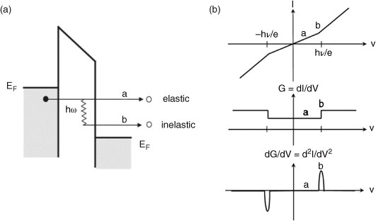
Figure 11.7 (a) Energy band diagram of a tunnel junction with a vibrational mode of frequency ω localized inside: “a” is the elastic tunneling process; “b” is the inelastic tunneling process. (b) Corresponding I(V), dI/dV, and d2I/dV2 characteristics. Reproduced with permission from [99]. Copyright 2008 Elsevier
IETS recently became a primary characterization technique to identify the component molecules present in molecular junctions (not an adlayer or impurity, but molecules forming the active region of a junction) [103–106], analogous to infrared and Raman spectroscopy for macroscopic samples, for the unambiguous determination of the molecular species in the junction. An example of experimental IETS measurements is shown in Figure 11.8 [106], which shows the I(V) curve, the differential conductance (dI/dV), and the IETS (d2I/dV2) spectrum of Au-octanedithiol (ODT)-Au and Au-benzenedithiol (BDT)-Au junctions measured at 4.2 K using an electromigrated break junction. Although the I(V) characteristics seem to be linear over the bias range measured, the plots of dI/dV and d2I/dV2 exhibit significant features corresponding to vibrational modes of the molecules under investigation. Standard AC modulation techniques with a lock-in amplifier are used to directly obtain the first and second harmonic signals proportional to dI/dV and d2I/dV2, respectively [107]. As explained above, a molecular vibration coupled to tunneling charge carriers gives rise to an increase in slope of the dI/dV curve owing to an inelastic tunneling process, which then appears as a step and peak in the first (dI/dV) and second (d2I/dV2) derivatives, respectively. The plot of d2I/dV2 versus V is referred to as the IETS spectrum. The observed spectral features were assigned to specific molecular vibrations by comparison with previously reported infrared, Raman, and IETS measurements and by density functional theory calculations. For the ODT junction (Figure 11.8c), peaks were reproducibly observed at 92, 119, 143, 161, 181, and 355 mV, which correspond to ν(C-S) stretching, δr(CH2) rocking, ν(C-C) stretching, γw(CH2) wagging, δs(CH2) scissoring, and ν(C-H) stretching modes, respectively. The absence of a prominent peak corresponding to the ν(S-H) stretching mode at 319 mV (2575 cm−1) suggests that the thiol (–SH) anchoring group reacts with the Au electrode pairs broken during the electromigration. In the IETS spectrum of the BDT junction (Figure 11.8f), three prominent peaks reproducibly appeared at 96, 142, and 201 mV, corresponding to γ(C–H) aryl out of plane bending, ν(18a) stretching, and ν(8a) stretching modes, respectively. These modes originate from vibrations of the phenyl ring. A theoretical study predicted that the ν(18a) and ν(8a) ring modes should have strong vibronic coupling in phenylene molecules [108] and is consistent with these results. The dominance of aromatic ring modes in IETS spectra has also been experimentally observed for various conjugated molecules [109,110]. The fully assigned IETS spectrum provides unambiguous experimental evidence of the existence of the desired molecules in the region of the junction and, correlating with the other characteristics of the junction transport, only leaves the IETS-identified molecule as the only element in the junction through which tunneling is occurring.
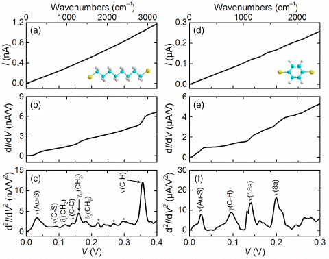
Figure 11.8 Transport properties of gold junctions measured at 4.2 K: (a)–(c) Au-ODT-Au and (d)–(f) Au-BDT-Au. (a) and (d) I(V) characteristics. The insets display the chemical structure of each molecule. (b) and (e) Differential conductance (dI/dV) obtained from lock-in first harmonic signal. (c) and (f) IETS spectrum (d2I/dV2) obtained from lock-in second harmonic signal. The peaks are labeled with their assigned vibrational modes. Reproduced with permission from [106]. Copyright 2009 American Institute of Physics
The first observation of IETS in a single molecule was obtained in STM [111]. The possibility of performing IETS studies using STM was discussed soon after its invention [112]. However, due to difficulties in achieving the extreme mechanical stability that is necessary to observe small changes in tunneling conductance, this technique has only recently been realized [111]. In the STM implementation of IETS, the MIM tunnel junction is replaced by a STM junction consisting of a sharp metallic tip, a vacuum gap, and a surface with the adsorbed molecules. Using STM-IETS, elegant imaging and probing can be performed at the same time, and vibrational spectroscopy studies on a single molecule can be achieved [113]. One of the most fruitful techniques for IETS of molecular structures arose from the pioneering work of Gregory [114] in 1990, in which a junction between two crossed wires was delicately made by a deflecting Lorentz force. Kushmerick et al. [115] demonstrated that reproducible molecular junctions could be formed with sufficient stability and robustness for clear IETS signatures [109]. The ease of electrode and molecular exchange has allowed elegant and thorough investigations of structure–function relationships. The technique has also enabled investigations into such areas as selection rules [116] and pathways [117], illustrating the power of IETS in characterizing and understanding nanoscale junctions. Wang et al. also reported an IETS study of an alkanedithiol self-assembled monolayer (SAM) using a nanometer-scale device (nanopore technique) [103]. Remarkably, the authors were able to verify that the observed spectra were indeed valid IETS data by examining the peak width as a function of temperature and AC modulation voltage (refer to the following paragraph) [103]. Recently, Hihath et al. [118] reported the IETS spectra of a single 1,3-propanedithiol molecule using an STM break junction at cryogenic temperatures. In particular, these authors were able to observe simultaneous changes in the conductance and vibrational modes of a single molecule as the junction was stretched. This ability allowed them to correlate the changes in the conductance with the changes in the configuration of a single-molecule junction. Moreover, the authors were also able to conduct a statistical analysis of the phonon spectra to identify the most relevant modes. These vibrational modes matched the IR and Raman spectra well and have been described by a simple one-dimensional model [118]. Another useful example of IETS for studying molecular junctions was reported by Long et al. [110] This study provides insight into changing transport characteristics resulting from exposure to air. IETS spectra have shown that molecular conduction could be significantly affected by rapid hydration at the gold–sulfur contacts. The detrimental effects of hydration on molecular conduction are important for understanding charge transport through gold–thiol molecular junctions exposed to atmospheric conditions.
An important tool to verify that the obtained spectra are indeed valid IETS data is to examine the vibrational peak width broadening as a function of temperature and applied modulation voltage. The width of a spectral peak includes a natural intrinsic linewidth, WI, and two broadening effects: thermal broadening (5.4kBT/e, where kB is Boltzmann's constant and T denotes temperature) due to the breadth of the Fermi level and modulation broadening (1.7Vm, where Vm is the AC modulation voltage) due to the dynamic detection technique used to obtain the second harmonic signals [119]. The full width at half maximum (FWHM) of the d2I/dV2 vibrational peak in IETS is given by [98,120]:
Figure 11.9 illustrates a study of the linewidth broadening of a vibrational peak in IETS measurements. Figure 11.9a shows the modulation broadening of a representative IETS feature {from Reference [16, the ν(C–H) stretching mode of ODT molecules in the electromigrated break junction} at a constant temperature of 4.2 K. The data points show the FWHM of the experimental peak. Considering the known thermal broadening and modulation broadening, the intrinsic linewidth, WI, can be determined from a fit to the modulation broadening data (Figure 11.9a, solid line), giving WI = 4.94 ± 0.89 meV (following Equation 11.3). Figure 11.9b shows the thermal broadening of the same ν(C–H) peak at a fixed modulation, demonstrating excellent agreement between the experimental FWHM values (circles) and theoretical values (squares).
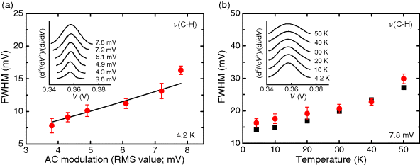
Figure 11.9 Full width at half maximum (FWHM) of the peak corresponding to the ν(C–H) stretching mode (∼357 mV) as a function of AC modulation voltage (a) and temperature (b). The circles indicate experimental data, and the solid line (a) and squares (b) show theoretical values. The error bars are determined by the Gaussian fitting. Insets show successive IET spectroscopy scans for the ν(C–H) mode under increasing AC modulation voltage (a) and increasing temperature (b), as indicated. r.m.s., root mean squared. Reproduced with permission from [16]. Copyright 2009 Nature Publishing Group
Over the last few years, IETS has evolved into an essential tool in the field of molecular electronics. Although IETS requires cryogenic temperatures, it is the only available method that provides both structural and electronic information about a single-molecule electronic device for a particular conformation and contact geometry of the molecular junction at low temperature [8]. From sophisticated comparisons between experiments and theoretical computations, IETS can be more useful for characterizing numerous aspects of molecular junctions, such as identification of the molecule, information on the nature of the interfaces, orientation of the molecule, and even electronic pathways [2].
Recently an additional tool, transition voltage spectroscopy (TVS), became an increasingly popular spectroscopic tool for molecular junctions [16,121–125] and other diverse nanoelectronic systems [126]. Specifically, TVS is used to give insight into the energy offset between the contact Fermi level and the nearest molecular level responsible for charge transport in molecular junctions by measuring the transition voltage (Vtrans) required to generate the inflection behavior of a Fowler–Nordheim (F-N) plot, that is, the corresponding analysis of ln(I/V2) against 1/V for I(V) characteristics [121,122].
By combining TVS with ultraviolet photoelectron spectroscopy (UPS), Beebe et al. [121] correlated the charge transport properties of π-conjugated molecules with their effective band lineup. In this study, CP-AFM and crossed-wire tunnel junction measurements on molecular junctions revealed a characteristic minimum in the F-N plot at a bias voltage, Vtrans (Figure 11.10a), which scaled linearly with the HOMO energy (which is the nearest molecular level for the measured molecules) obtained from UPS (Figure 11.10b) [121]. These results show that the magnitude of Vtrans is molecule-specific (as a form of spectroscopy) and depends directly on the manner in which the conjugation path is extended. In general, the HOMO–LUMO gap of π-conjugated molecules decreases with an increase in conjugation length [127]. It is thus reasonable to expect longer conjugated molecules to exhibit a smaller value of Vtrans than shorter conjugated molecules within a given molecular series [122]. Recently, TVS also facilitated the calibration of orbital energy positions in molecular transistors [16,128].
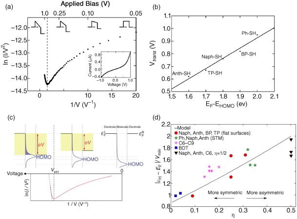
Figure 11.10 (a) Solid circles represent the average of 100 I–V curves for an Au-anthracenethiol-Au junction measured by CP-AFM. The dashed line corresponds to the voltage at which the tunneling barrier transitions from trapezoidal to triangular (Vtrans). Also shown are representations of the barrier shape at various values of applied bias. The inset shows current-voltage data on standard axes. (b) Vtrans (CP-AFM) versus EF-EHOMO energy difference (UPS). Reproduced with permission from [121]. Copyright 2006 American Physical Society. (c) Schematic of the theoretical model [129] to qualitatively explain the inflection of F-N curve. Also shown are representations of the barrier shape at various values of applied bias. The inset shows current–voltage data on standard axes. Reproduced with permission from [129]. Copyright 2010 American Physical Society. (d) Ratio between the HOMO energy (at zero bias) and the transition voltage, (denoted as Vmin in the figure), versus asymmetry parameter, η. The solid line is obtained from a Lorentzian transmission function and symbols are results of ab initio finite bias calculations (see Reference [130] for details). Reproduced with permission from [130]. Copyright 2010 American Physical Society
TVS was initially interpreted by a simple barrier picture for charge tunneling in a junction [121]. Within this interpretation, the transition behavior in the F-N plots corresponds to a change in the tunneling mechanism from direct tunneling through a trapezoidal barrier to Fowler–Nordheim tunneling (or field emission) through a triangular barrier (see the barrier shapes in Figure 11.12a) [121]. The transition voltage equals the barrier height, which is interpreted as the energy gap from the metal electrode's Fermi level to the nearest molecular level. However, as pointed out by Huisman et al. [124], the naïve tunnel barrier model is inconsistent with experimental data. On the other hand, the TVS experiments on molecular junctions are more appropriately described by the coherent Landauer approach with a single transport level [124]. Charge transport through such a junction is described by a transmission function, which is assumed to have a Lorentzian shape. Within the coherent Landauer transport picture, Vtrans can be directly scaled with the barrier height (ΦB) in molecular junctions, thus giving valid information on molecular energy levels. Araidai et al. [129] theoretically investigated the origin of an inflection behavior appearing in the F-N plot of I(V) characteristics for molecular junctions. The results show that the inflection does not necessarily indicate the transition between the two regimes of direct tunneling and Fowler–Nordheim tunneling. Their close examination of the relation between the behavior of the F-N curve and the transmission function showed that the inflection takes place when the molecular level responsible for the charge transport approaches the edge of the electrode-bias window (Figure 11.10c) [129]. Although the origin of the inflection behavior drastically differs from the conventional model, the F-N plots obtained from their calculations show very similar behavior to those from recent experiments [129]. Recently, Chen et al. [130] reported extensive ab initio calculations to simulate TVS for a broad class of molecular junctions. The numerical data closely follow the trend expected from an analytical model with a Lorentzian-shaped transmission function. Interestingly, the ratio of Vtrans to the HOMO level position was found to vary between 0.8 and 2.0 depending on the junction asymmetry (as shown in Figure 11.10d), which means that it is necessary to consider the asymmetry of the molecular junction to use TVS as a quantitative spectroscopic tool to probe the molecular levels [130].
The interpretation of TVS, fulfilled by comparison of the Simmons model and the coherent Landauer approach, suggests that length-dependent TVS measurements for saturated alkyl chains can provide a critical test to distinguish true molecular junctions from a vacuum tunnel junction with no molecules [124]. The saturated alkyl molecular system constitutes an important control series in molecular transport experiments to corroborate valid molecular junctions because molecular energy levels remain nearly unchanged with molecular length, and the transport mechanism has been extensively established. To this end, TVS on a series of alkanedithiol molecules having different lengths (ranging from DC8 to DC12) was performed, employing electromigrated break junctions [87]. Vtrans for a series of alkanedithiol molecules is summarized graphically in Figure 11.11a. The average value of Vtrans, represented by the solid line in Figure 11.11a, falls within the standard deviation (within two dashed lines) of measured values for each of the molecules, thereby illustrating that Vtrans is invariant with molecular length for alkanedithiols. This result is consistent with the fact that the HOMO–LUMO gap of these molecules is virtually length independent. Thus, this result agrees with the data of Beebe et al. [122]. Similarly, ultraviolet photoelectron spectroscopy measurements have shown that the energy offset between the HOMO and the electrode's Fermi level for different length alkyl chains is constant [131,132]. It should be noted that such length constancy in Vtrans for the alkanedithiol junctions is fully in agreement with the results expected from a coherent molecular transport model based on the Landauer formula, that is, Vtrans is independent of molecular length (longer than ∼8 Å) for constant barrier heights (ΦB; see Figure 11.11b) [124]. These findings on length-dependent TVS measurements provide additional verification of the formation of a true molecular junction [87].
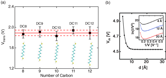
Figure 11.11 (a) Vtrans as a function of molecular length for a series of alkanedithiols from DC8 to DC12. The solid line represents the mean value of Vtrans for five different length alkanedithiols, and two dashed lines show the standard deviation for averaging. Error bars on each data point also denote the standard deviation across individual measurements for different devices. Chemical structures for each molecule are displayed in the inset. Reproduced with permission from [87]. Copyright 2010 American Chemical Society. (b) Vtrans (denoted as Vm in the figure) versus molecular length d. Vtrans becomes length independent for d > 8 Å. Reproduced with permission from [124]. Copyright 2010 American Chemical Society
An additional technique, thermopower (also called the Seebeck coefficient, S), has been utilized to investigate single molecule junctions. Paulsson and Data stressed in a theoretical paper that thermoelectric measurements can provide new insights into charge transport in molecular junctions [133]. Analogous to the hot point probe measurements commonly used to establish the p- or n-type character of semiconductors [134], the thermoelectric voltage yields valuable information regarding the location of the Fermi energy. Previous proposals have suggested that the location of the Fermi energy can be deduced from the asymmetry of the I(V) curve caused by asymmetric contacts [135]. However, this measurement is performed far from equilibrium and requires detailed knowledge of the contacts [133]. In contrast, the thermoelectric voltage in molecular junctions is large enough to be measured but is rather insensitive to the detailed coupling to the contacts, and it gives valuable information about the position of the Fermi energy relative to the molecular levels [133]. Interestingly, these thermoelectric measurements suggest that a molecular junction could be the basis for not only molecular electronics but also thermoelectric energy conversion devices [136].
The first experiment on the thermoelectric measurement in single-molecule junctions was reported by Reddy et al. in 2007 [136]. These authors used STM break junctions to trap molecules between two gold electrodes with a temperature differential and statistically measured the thermoelectric voltage of 1,4-benzenedithiol (BDT), 4,4-dibenzenedithiol (DBDT), and 4,4-tribenzenedithiol (TBDT) in contact with gold at room temperature. These data were used to construct histograms for each temperature differential, which were used to estimate the average and the variation in the junction thermopower (or Seebeck coefficient), Sjunction.
The relation between Sjunction of the Au-molecule-Au junction and the measured thermoelectric voltage, ΔV, is given by [136]:
where SAu is the Seebeck coefficient of bulk Au, which is 1.94 μV/K at 300 K [137]. ΔVpeak is plotted as a function of ΔT, where ΔVpeak corresponds to ΔV at the peak of the distribution in the histogram. From the slope ΔVpeak/ΔT and Equation 11.4, it was found that SAu-BDT-Au = +8.7 ± 2.1 μV/K, where the error is the FWHM [136]. Similar experiments were also performed with DBDT and TBDT, and statistical analysis revealed that SAu-DBDT-Au = +12.9 ± 2.2 μV/K and SAu-TBDT-Au = +14.2 ± 3.2 μV/K [136]. There seems to be a linear dependence of the thermopower with molecular length, which is in contrast to the exponential dependence of electrical resistance that is generally attributed to tunneling across the molecule. The relative position of the HOMO and LUMO levels with respect to the EF of the metal electrodes can be related to the measured value of Sjunction [133]. The Landauer formula [138] is used to relate Sjunction to the transmission function, τ(E). It is shown that Sjunction can be obtained as [136]:
where kB is the Boltzmann constant. The transmission function for the case of the Au-BDT-Au junction, which was derived using the nonequilibrium Green's function formalism in conjunction with the extended Huckel theory [133]. It is clear that τ(E) ∼ 1 when EF aligns with either the HOMO or the LUMO levels and decreases rapidly to below 0.01 in between [136]. Using this transmission function in Equation 11.5, it was shown that, depending on the position of the Fermi energy with respect to molecular levels, the thermopower can be either positive or negative. If EF is closer to the HOMO, the sign is positive, indicative of hole-dominated transport. If, on the contrary, the LUMO is closer to EF, then the thermopower is negative, indicative of electron-dominated transport. SAu-BDT-Au is positive (p-type), and thus, EF is closer to the HOMO level (hole-dominated transport) [136]. Using the measured value of SAu-BDT-Au = +8.7 ± 2.1 μV/K from Figure 11.14c, EF was also estimated to be 1.2 eV from the HOMO level [136].
Baheti et al. [139] also performed thermopower measurements to elucidate the effects of chemical structure on the electronic structure and charge transport in molecular junctions. Again, the authors used a STM break-junction technique to measure the Seebeck coefficient of several benzene derivatives, where 1,4-benzenedithiol (BDT) was modified by the addition of electron-withdrawing or electron-donating groups such as fluorine, chlorine, and methyl on the benzene ring, and the thiol end groups on BDT were replaced by cyanide end groups [139]. For the substituted BDT molecules, it was observed that the thermopower of the molecular junction decreases for electron-withdrawing substituents (fluorine and chlorine) and increases for electron-donating substituents (methyl) [139]. In fact, this change in the measured thermopower is reasonably predictable. Electron-withdrawing groups remove electron density from the σ-orbital of the benzene ring, allowing the ring's high-energy π system to stabilize. Because the HOMO has a largely π character, its energy is therefore decreased, shifting it further away from EF. As discussed above, such a shift results in a decrease of the thermopower. Alternatively, the addition of electron-donating groups increases the σ-orbital electron density in the benzene ring, leading to an increase in the energy of the π-system and thereby shifting the HOMO closer to EF. This shift causes the enhancement of the thermopower in this case. Moreover, the sign of the thermopower for cyanide end groups were found to be negative, which indicates that charge transport in 1,4-benzenedicyanide is dominated by the LUMO [139]. Thus, these measurements show that it is possible to tune the thermoelectric properties of molecular junctions in a controllable way by the addition of substituents.
Combined optical and transport experiments on molecular junctions can reveal a wealth of additional information beyond that available from purely electronic measurements [140]. Exciting recent works have demonstrated that simultaneous single-molecule optical spectroscopy and transport measurement is possible [140–142]. These experiments are based on the fact that the metallic nanogap electrodes used to create molecular junctions are able to act as tremendously effective plasmonic antennas, leading to dramatic surface-enhanced Raman scattering in the junctions [141,142], which thus makes it possible to perform surface-enhanced Raman spectroscopy (SERS) of a target molecule placed on the nanogaps (for a review of SERS, see Reference [143]).
Ward et al. [140–142,144] performed a series of optical experiments on Au nanogap structures prepared with electromigration using a confocal Raman microscope. The initial experiments examined nanogaps as a potential SERS substrate [141], with para-mercaptoaniline (pMA) as the molecule of interest. Nanoconstrictions were placed in parallel to allow the simultaneous electromigration of seven nanogaps at one time (Figure 11.12a). Samples were characterized using a Raman microscope via spatial maps and time spectra of the SERS response. Prior to electromigration, no significant SERS response was detected anywhere on the devices. Following electromigration, the authors observed a SERS response that was strongly localized to the resulting gaps. Successive spectra measured directly over the SERS hotspot revealed “blinking” and spectral diffusion, phenomena often associated with single- or few-molecule Raman sensitivity [141]. Blinking occurs when the Raman spectrum rapidly changes on the second timescale, with the amplitudes of different modes changing independently of one another. Spectral shifts as large as ±20 cm−1 were observed, making it difficult to directly compare SERS spectra with other published results. Blinking and spectral shifts are attributed to the movement or rearrangement of the molecule relative to the metallic substrate. It is unlikely that an ensemble of molecules would experience the same rearrangements synchronously, and thus the observation of blinking and wandering is expected only in situations where a few molecules are probed [141].
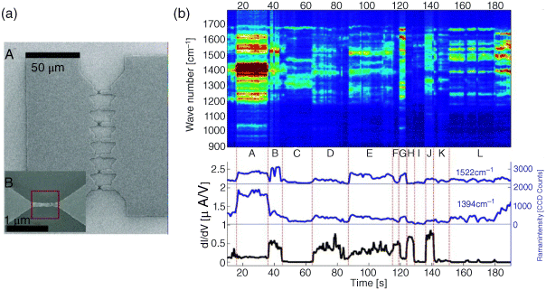
Figure 11.12 (a) Micrograph A: Full multibowtie structure, with seven nanoconstrictions. Inset B: Close-up of an individual constriction after electromigration. Note that the resulting nanoscale gap (<5 nm at closest separation, as inferred from closer images) is toward the right edge of the indicated red square. Reproduced with permission from [141]. Copyright 2010 American Chemical Society. (b) Waterfall plot of Raman spectrum (1 s integrations) and conduction measurements for a pMA sample. The device experiences periods of correlation (regions B, D, E) and anticorrelation (region L) between Raman intensity and conduction. Distinct changes in conduction are observed with every significant change in the Raman spectrum and are indicated by vertical lines. The modes near 1394 and 1522 cm−1 show similar intensity fluctuations except at region B and the end of region L. This results in the saturation of the signal at region A which would otherwise resolve into well-defined peaks. The 1522 cm−1 mode has been shifted upward on the lower graph for clarity. Reproduced with permission from [142]. Copyright 2010 American Chemical Society
In a subsequent experiment [142], the same group performed simultaneous SERS and transport measurements, including Raman microscope observations over the center of nanogap devices during electromigration. Molecules of interest, pMA or a fluorinated oligomer (FOPE), were assembled on the Au surface prior to electromigration. Once the device resistance exceeded approximately 1 kΩ, SERS could be seen. This result indicates that localized plasmon modes responsible for the large SERS enhancements may now be excited. As the gap migrates further, the SERS response scaled logarithmically with the device resistance until the resistance reached approximately 1 MΩ. In most samples, the Raman response and conduction of the nanogap become decoupled at this point, with the conduction typically changing little while uncorrelated Raman blinking occurs. In about 11% of 190 devices, however, the Raman response and conduction showed very strong temporal correlations [142]. A typical correlated SERS time spectrum and conductance measurement for a FOPE device are presented in Figure 11.12b. Because the conduction in nanogaps is dominated by approximately a single molecular volume, the observed correlations between conductance and Raman measurements strongly indicate that the nanogaps have single-molecule Raman sensitivity. It is then possible to confirm that electronic transport is taking place through the molecule of interest from the characteristic Raman spectrum. Data sets such as those shown in Figure 11.12b implicitly contain an enormous amount of information about the configuration of the molecule in the junction [140].
Tian et al. [36] reported a combined SERS and mechanically controllable break-junction method to measure the SERS signals of molecules located inside the nanogap between two electrodes on a Si chip [874]. They showed that the SERS signal depends critically on the separation of the electrodes and the incident light polarization. In particular, when the incident laser polarization was along the two electrodes, the field in the nanogap was the strongest because of the coupling to the localized surface plasmon resonance of the two gold electrodes [145]. Moskovits and colleagues carried out SERS measurements on Rhodamine (R6G) adsorbed in nanogaps produced in single Ag nanowire by electromigration [146]. For gaps that divide the nanowire uniformly across its width, the SERS intensity was maximum when the electric vector was oriented parallel to the long axis of the nanowire (i.e., across the gap). In the experiment of Ioffe et al. [147], SERS was also used as a tool to spectroscopically monitor heating (and cooling) processes in conducting molecular junctions, which involved measuring both the Stokes and anti-Stokes components of the Raman scattering.
11.3 Molecular Transistors
11.3.1 Orbital Gated Transport
Theoretical proposals have indicated that the field-effect gating of a molecular junction is possible in a fashion similar to a conventional field-effect transistor (FET) [148–152]. Indeed, the experimental demonstration of a true molecular transistor, one that depends on the external modulation of molecular orbitals, has been the outstanding challenge of the field of molecular electronics since soon after its inception [1].
We recently presented the construction and characterization of molecular transistors [16], where the transport current is controlled by directly modulating the energy of the molecular orbitals of a single molecule (based purely on electrostatic gate control). As illustrated in Figure 11.13a, individual molecules are connected to source and drain electrodes with a bottom-gate control electrode in a FET configuration. In such devices, the energies of the molecular orbitals with respect to the Fermi level of the electrodes can be directly tuned by adjusting the gate voltage, VG. We made such devices using the electromigration technique of fracturing a continuous gold wire (coated with the desired molecules in vacuum at 4.2 K) that is placed over an oxidized aluminum gate electrode [14,45,153]. This arrangement produces source and drain electrodes with a nanometer-scale gap that are often bridged by single or very few molecules.
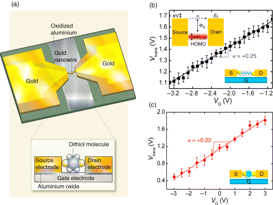
Figure 11.13 (a) Schematic illustration of a molecular transistor. Diagram A: Each device consists of a fractured gold nanowire overlaid on a strip of oxidized aluminum. Inset B: Side-on, close-up view of a device. The broken ends of the nanowire form the source and drain electrodes of the transistor, and the oxidized aluminum forms the gate electrode. Aluminum oxide on the surface of the gate electrode provides a necessary layer of insulating material known as the gate dielectric. A single molecule (here, an aromatic dithiol) connects the source and drain electrodes. The components of the device are not drawn to scale. Reproduced with permission from [144]. Copyright 2010 Nature Publishing Group. (b) Linear scaling of Vtrans in terms of VG for 1,8-octanedithiol. Inset: Schematic of the energy band for HOMO-mediated hole tunneling, where eVG,eff describes the actual amount of molecular orbital shift produced by gating. (c) Linear scaling of Vtrans in terms of VG for 1,4-benzenedithiol. Reproduced with permission from [16]. Copyright 2010 Nature Publishing Group
We verified that the charge transport properties were through the inserted molecules, using a combination of transport techniques that gives a self-consistent characterization of the molecular junction [16]. Inelastic electron tunneling spectroscopy (IETS) was used to measure the interactions between the tunneling charge carriers and the vibrational modes of the molecules in the devices. This technique provides definitive proof that the measured currents actually pass through the molecules in molecular transistors. We tested two types of transistor, each with a different molecule in the junction: either an alkanedithiol (containing two SH groups connected by a saturated hydrocarbon chain) or an aromatic dithiol (containing two SH groups connected by a benzene ring). Because each dithiol has its own vibrational fingerprint (see Figure 11.14), the IETS spectra of the devices provide unambiguous identification of the component molecules in the junctions.
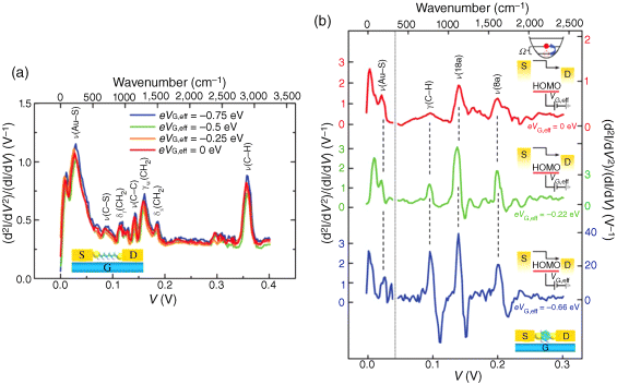
Figure 11.14 (a) IETS spectra for a Au-ODT-Au junction measured at 4.2 K for different values of eVG,eff, with vibration modes assigned. (b) IETS spectra for a Au-BDT-Au junction measured at 4.2 K for different values of eVG,eff, with vibration modes assigned. The left-hand y axis corresponds to the left shaded region of the spectra, and the various right-hand y axes (with different scales) correspond to the related spectra in the right region. The vertical dotted line corresponds to V = 45 mV (363 cm−1). Significant modification in the spectral intensity and line shape for the benzene ring modes, g(C–H), n(18a) and n(8a), was observed for different values of eVG,eff, as indicated. Insets: Energy diagrams illustrating inelastic tunneling as the position of the HOMO resonance shifts as a result of gating. Reproduced with permission from [16]. Copyright 2010 Nature Publishing Group
Transition voltage spectroscopy (TVS), which measures the transition voltage (Vtrans) required to generate inflection behavior in a Fowler–Nordheim plot was also used. It has previously been shown [121,122] that Vtrans is proportional to the difference in energy between the gating orbital of the molecular junction (the orbital that modulates charge transport) and the Fermi levels of the source and drain electrodes, where the Fermi level is the highest possible energy for a conducting electron in an electrode. By measuring Vtrans using TVS at different applied gate voltages, we demonstrated that a linear relationship exists between the gate voltages and molecular orbital energy in their devices (Figure 11.13b and c), as expected for molecular transistors [128]. The slope in the linear relationship, α = ΔVtrans/ΔVG, is the gate efficiency factor, which describes the effectiveness of molecular orbital gating. The actual amount of molecular orbital shift produced by the applied gate voltage can also be determined in terms of an effective molecular orbital gating energy, eVG,eff = |α|eVG. In a three-terminal device, a negative or positive gate voltage would respectively raise or lower the orbital energies in the molecules relative to EF [149,150]. Therefore, a positive value of α indicates HOMO-mediated hole tunneling (p-type-like; Figure 11.13b, inset). Conversely, α is negative for LUMO-mediated electron tunneling (n-type-like). By extrapolating the y-intercept from the linear fit in Figure 11.13b, Song et al. obtained the zero-gate transition voltage, Vtrans,0 = 1.93 ± 0.06 V for Au-octanedithiol (ODT)-Au junctions, which provides an estimate of the original position (at VG = 0 V) of the HOMO level relative to EF. For Au-benzenedithiol (BDT)-Au junctions, the positive sign of α explicitly indicates that HOMO-mediated tunneling is the dominant transport channel (Figure 11.13c). It was found to be Vtrans,0 = 1.14 ± 0.04 V for the BDT junction, which is much less than the value for the ODT junction owing to the π-conjugated BDT molecule having a smaller HOMO–LUMO gap.
We further examined the dependence of the IETS spectra on molecular orbital gating [16]. The IETS spectra of the transistors that incorporate alkanedithiol (ODT) were essentially unaffected by the gate voltage (Figure 11.14a). This finding indicates that charge transport through the device is nonresonant; that is, there is a large energy difference between the dithiol's HOMO and the electrode's Fermi level. Conversely, we observed that the applied gate voltage strongly modulates the IETS spectra of transistors that incorporate an aromatic dithiol (BDT; Figure 11.14b) [16]. Specifically, when a negative gate voltage is applied (which brings the energy of the molecular junction's HOMO closer to that of the electrode's Fermi level), the signal intensities of the spectra increase greatly and the shapes of the vibrational peaks change. The change in peak shape is a clear indication of increased coupling between the tunneling charge carriers and the molecular vibrations, owing to a near resonance between the HOMO and the Fermi level [154,155].
Collectively, these results demonstrate direct gate modulation of molecular orbitals in molecular transistors. The IETS spectra reveal which orbitals are resonantly enhanced, and dramatic differences are seen in the comparison between near resonant and far from resonant systems. These observations validate the concept of orbital-modulated carrier transport and elucidate both charge transport mechanisms and the electronic structure of molecular junctions.
Subsequently, Cao et al. [156] reported electrode structures with a controllable molecular-scale gap between source and drain electrodes and a third terminal of a buried gate using photolithography and molecular lithography with self-assembled mono/multiple molecule layer(s) as a resist. The synthesized thiolated phthalocyanine-derivative molecules were assembled between the tailored molecular gap of the fabricated FET electrode structures in solution via Au-S bonding, forming stable contacts between the electrodes and the molecules [156]. The electrical measurements at room temperature show that the device has transport characteristics of a typical p-type FET device with large gate modulation [156]. In addition, the transistor effect has been also observed at a monolayer level, for example, for alkanethiol [157] and various conjugated molecules [158–160].
11.3.2 Coulomb Blockade and Kondo Regimes
Solid-state molecular transistors have been used to study two additional mechanisms in single molecule quantum dots [13–15,45–47,153]: Coulomb blockades, in which the flow of electrons is controlled by the sequential charging of a molecule due to electron–electron Coulomb repulsion, and the Kondo effect, in which conducting electrons interact with the local spin (intrinsic angular momentum) of the quantum dot in a molecular junction, leading to an increase of the conductance at low bias.
For example, a Coulomb blockade was observed for molecules such as fullerene (C60) [13] and p-phenylenevinylene oligomers [15], which have five benzene rings connected through four double bonds (OPV5) weakly coupled to the source-drain electrodes. Park et al. [13] prepared a single-C60 transistor by depositing a dilute toluene solution of C60 onto a ∼1 nm gap between gold electrodes created by electromigration. The entire structure was defined on a SiO2 insulating layer on top of a degenerately doped silicon wafer, which served as a gate electrode that modulated the electrostatic potential of the C60 molecule. The devices exhibited strongly suppressed conductance near zero bias voltage followed by steplike current jumps at higher voltages. These transport features clearly indicate that the conduction in this device is dominated by the Coulomb blockade effect. From analysis of the stability diagram in Figure 11.15a (conductance plots as a function of the bias voltage and the gate voltage), Park et al. [13] showed that the charging energy of the C60 molecule can exceed 150 meV. This value is much larger than in semiconductor quantum dots. Notice that in the stability diagrams of Figure 11.15a, there are running lines (marked by arrows) that intersect the main diamonds or conductance gap regions, indicating the presence of internal excitations of the C60 molecules. The energies of these excitations (of a few meV) are too small to correspond to electronic excitations. The authors of Reference [13 suggested that these lines could correspond to the vibrational excitation of the center of mass oscillation of C60 within the confinement potential that binds it to the gold surface. In the case of OPV5, Kubatkin et al. [15] observed up to eight successive charge states of the molecule, as shown in Figure 11.15b. This result suggests that the transport experiment had access to many different charge or redox states. While the spectroscopic HOMO–LUMO gap for this molecule is of the order of 2.5 eV, the extracted gap from the stability diagram in Figure 11.15b is one order of magnitude smaller (0.2 eV). The authors argued that this discrepancy is due to the fact that the intrinsic electronic levels of the molecules are significantly altered in the metallic contacts. In particular, they suggested that the image charges generated in the source and drain electrodes by the charges on the molecule are probably the origin of this effect. With organometallic molecules bearing a transition metal, such as the cobalt terpiridynil complex and divanadium complex, Kondo resonance has been observed in addition to Coulomb blockades [14,45]. Kondo resonance is observed when increasing the coupling between the molecule and the electrodes (e.g., by changing the length of the insulating tethers between the metal ion and the electrodes) [14]. van der Zant et al. and Natelson et al. have achieved much in this field, such as transport measurements through single molecular magnets [161], the observation of the Kondo effect in gold break junctions with the presence of magnetic impurities [162], inelastic tunneling features via molecular vibrations in the Kondo regime [163], and fundamental scaling laws that govern the nonequilibrium standard spin–1/2 Kondo effect [164]. We recommend the following reviews on this subject: References [46,47,165–167].
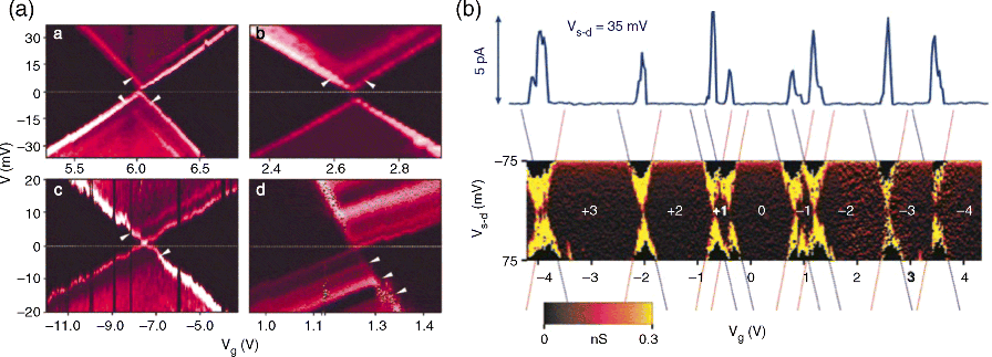
Figure 11.15 (a) Different conductance plots as a function of the bias voltage and the gate voltage obtained from four different devices. The dark triangular regions correspond to the conductance gap, and the bright lines represent peaks in the differential conductance. The arrows mark the point where the conductance lines intercept the conductance gap. Reproduced with permission from [13]. Copyright 2000 Nature Publishing Group. (b) Measurements of the differential conductance for OPV5 as a function of the bias voltage and the gate voltage. The full solid line at the top of the figure shows a representative I(V) trace. Reproduced with permission from [15]. Copyright 2003 Nature Publishing Group
Several groups have also demonstrated the FET-like behavior of redox molecules using an electrochemical gate [168–170]. This method has the advantage that the potential at the molecule is well-defined because the potential drop at each electrode is maintained by a double layer established with respect to a reference electrode [5]. Because the gate voltage falls across the double layers at the electrode–electrolyte interfaces, the effective gate thickness is in the order of a few solvated ions, which results in a large gate field. This large field allows the reversible switching of redox molecules between oxidized and reduced states. For example, a study of perylene tetracarboxylic diimide (PTCDI), a redox molecule, found that the current through the molecule can be reversibly varied over nearly three orders of magnitude [169]. In terms of the energy diagram, decreasing the gate voltage shifts the LUMO of the PTCDI redox molecule towards the Fermi levels of the electrodes, causing a large increase in the current through the molecules (i.e., n-type FET-like behavior). Recently, Diez-Perez et al. [171] synthesized two coronene derivatives, each consisting of 13 aromatic rings arranged into a well-defined honeycomb structure. Using the STM break–junction method, they studied charge transport in single coronene molecules as a function of the electrochemical gate voltage and observed pronounced n-type gating effects in these single coronene devices [171].
11.4 Molecular Design
It is clear that the charge transport through a molecular junction crucially depends on the position of the frontier orbitals (HOMO or LUMO) of the molecule with respect to the electrode's Fermi energy and on its character (degree of delocalization). In principle, side groups or substituents can control the conformation of a molecule, which in turn determines the degree of conjugation (i.e., delocalization of the molecular orbitals), and they can adjust the position of the frontier orbitals (i.e., the intrinsic electronic structure of a molecule). All of these effects have a strong influence on the conductance of the molecular junction. Thus, the transport characteristics can be chemically tuned and designed, to a certain extent, with the inclusion of appropriate side groups or substituents.
Venkataraman et al. [172] measured the low-bias conductance values of a series of very short conjugated molecules (substituted 1,4-diaminobenzenes) using a STM-based break–junction technique in a solution of the molecules. Transport through these substituted benzenes was confirmed using coherent nonresonant tunneling or superexchange, with the molecular junction conductance depending on the alignment of the metal Fermi level to the nearest molecular level. Electron-donating substituents, which increase the energy of the occupied molecular orbitals, increase the junction conductance, while electron-withdrawing substituents have the opposite effect. In detail, the highest occupied molecular orbital (HOMO) in 1,4-diaminobenzene is best described as a combination of the lone pairs on each of the N atoms and some component of p–π density on each of the two C atoms to which the N atoms are bonded. As electron-donating substituents replace H atoms on the ring, the energy of the HOMO increases. When a H atom is replaced by a methoxy group (OCH3), the O(2pπ) lone pair delocalizes into the benzene π space, thereby raising the HOMO energy. On the contrary, when electron-withdrawing substituents replace H atoms, the energy of the HOMO is lowered. When H is replaced by Cl, the more electronegative Cl removes electron density from the σ space of the benzene, thereby deshielding the π space and lowering the HOMO energy. These shifts in the isolated molecule are measured as changes in the ionization potential (IP): electron-donating substituents decrease the IP, while electron-withdrawing substituents increase the IP. Thus, for the measured molecular series of the substituted 1,4-diaminobenzenes, the conductance values vary inversely with the calculated ionization potential of the molecules. These results reveal that the HOMO is closest to the gold Fermi energy, which is consistent with hole transport (i.e., transport dominated by the HOMO of the molecules) [172]. Interestingly, this study is consistent with the results reported by Baheti et al. [139], in which the thermopower of molecular junctions based on several 1,4-benzenedithiol (BDT) derivatives was investigated. The thermopower of the measured molecules was modified in the same way by the addition of electron-withdrawing or -donating groups such as fluorine, chlorine, and methyl on the benzene ring (see Section 11.3.4).
As shown in the example above, chemical modification via side groups or substituents can be used to control the alignment between the molecular levels and the Fermi energy of the metallic electrodes. In other words, one can use chemical substituents to “dope” molecular junctions. Another example of modulating conductance via chemical substituents was described in Reference [173], in which the authors examined the low-bias conductance of 1,4-bis-(6-thiahexyl)-benzene derivatives to study the correlation between the low-bias conductance and the position of the frontier orbitals. For this purpose, these authors theoretically determined the position of these orbitals using density functional theory (DFT) calculations. It was shown that the more electron-rich benzene rings (with a higher HOMO) have higher conductances, which is also consistent with hole transport (i.e., via the benzene HOMO). These results stress that the actual position of the frontier orbitals of the molecule in the junction are the true determinants of the conductance, which in principle may differ from the corresponding frontier orbitals in the gas phase. Thus, it would be highly desirable to obtain information about the molecular-level alignment with the electrode Fermi energy in molecular junctions. It is still rather challenging to show this fundamental effect in a systematic manner.
The fact that the molecular conformation must have a major impact on the conduction through a molecular junction has been reasonably predicted [174]. Some experiments have verified this effect [175], but the most illustrative example has been reported by Venkataraman et al. in Reference [91]. In the simple case of a biphenyl, a molecule with two phenyl rings linked by a single C–C bond, the conductance is expected to change with the relative twist angle between the two rings, with the planar conformation having the highest conductance. The authors used amine linking groups to form single-molecule junctions with a series of biphenyl molecules with different ring substitutions that alter the twist angle of the molecules. The two benzene rings of a biphenyl can rotate relative to each other. For such a molecule, as the twist angle (θ) between the two rings increases and the degree of π conjugation between them simultaneously decreases, the junction conductance is expected to decrease because molecular electron transfer rates scale as the square of the π overlap [174,176]. When neglecting the contribution of tunneling transport through the σ orbitals, the theory predicts a cos2 θ relation [177]. The authors of Reference [91] illustrated that the conductance for the biphenyl series decreases with increasing twist angle, consistent with the cosine-squared relation predicted for transport through π-conjugated biphenyl systems [177]. Specifically, Figure 11.16b shows the measured conductance histograms for the biphenyl molecules in Figure 11.16a. For the flat molecule (2), the histogram peak yields an average junction conductance value of 1.5 × 10⁻³G0 (G0 = 2e2/h, where e is the charge on an electron and h is Planck's constant). For 4,4′-diaminobiphenyl (4) with an equal molecular length but a twist angle θ of 34°, the conductance histogram shows a peak occurring at a lower conductance of 1.1 × 10⁻³G0. As the angle between the two aromatic rings is increased to 52° in 4,4′-diaminooctafluorobiphenyl (6), the conductance value also drops further, to 4.9 × 10⁻⁴G0. When all four hydrogen atoms on the proximal carbons of this molecule are replaced with methyl groups to give 2,6,2′,6′-tetramethyl-4,4′-diaminobiphenyl (8) with a twist angle θ of 88°, most counts in the histogram occur for low junction conductance values. Figure 11.16c shows a plot of the peak conductance value measured for the seven molecules against cos2 θ, and the data are fitted with a cos2 θ curve (dashed line in Figure 11.16c). The good quality of the fit indicates that the electronic effects of the substituents do not significantly alter the simple picture in which junction conductance may be adjusted by simply decreasing the π overlap between phenyl rings within the bridging molecule. However, the role of the geometric and electronic effects of the substituents is still being actively discussed [178,179].
Figure 11.16 Biphenyl junction conductance as a function of molecular twist angle. (a) Structures of a subset of the biphenyl series studied, shown in order of increasing twist angle or decreasing conjugation. (b) Conductance histograms obtained from measurements using molecule 2 (constructed from 15 000 traces and scaled by 1/15), molecule 4 (constructed from 7000 traces and scaled by 1/7), molecule 6 (constructed from 11 000 traces and scaled by 1/11) and molecule 8 (constructed from 5000 traces and scaled by 1/5). Also shown is the control histogram obtained from measurements without molecules between the contacts (constructed from 6000 traces and scaled by 1/6). Arrows point to the peak conductance values obtained from Lorentzian fits. All data were taken at a bias voltage of 25 mV. (c) Position of the peaks for all the molecules studied plotted against cos2θ, where θ is the calculated twist angle for each molecule. Error bars are determined from the standard deviation of the peak locations determined from the fits to histograms of 1000 traces. Reproduced with permission from [91]. Copyright 2006 Nature Publishing Group
Recently, Wandlowski and co-workers investigated the conductance of a family of biphenyl-dithiol derivatives with conformationally fixed torsion angles using the STM break–junction method [180]. They found that the measured conductance value depends on the torsion angle θ between two phenyl rings; twisting the biphenyl system from flat (θ = 0°) to perpendicular (θ = 90°) decreased the conductance by a factor of 30. Detailed calculations of transport based on DFT and a two-level model supported the experimentally obtained cos2 θ correlation between the junction conductance and the torsion angle.
In fact, the role of conjugation in the conduction through molecular systems has been clearly illustrated by the comparison of the conductance through alkanes to that through conjugated molecules with extended π electron states (e.g., oligophenyleneethynylene, OPE and oligophenylenevinylene, OPV). The π-conjugated molecules show substantially higher conductance than the alkanes, consistent with a rational dependence on the HOMO–LUMO gap [92,181].
The strength of the metal–molecule coupling can be also chemically tuned using appropriate anchoring groups to bind a molecule to metallic electrodes. Tao and coworkers have systematically studied the effect of anchoring groups on the conductance of single molecules using alkanes terminated with dithiol, diamine, and dicarboxylic acid groups as a model system [182]. The conductance values of these molecules were found to be independent of temperature, indicating coherent tunneling. For each anchoring group, the authors reported an exponential decay of the conductance with the molecular length, given by G = Aexp(−βN), which also suggests the tunneling mechanism. They observed differences in β between different anchoring groups with the trend β (dithiol) > β (diamine) ≥ β (dicarboxyl acid). The β values, ranging between 0.8 and 1.0 per –CH2 unit or between 0.6 and 0.8 Å−1, were close to the values reported in the literature [93]. The differences in β are small for the three anchoring groups, but this small difference can significantly affect long-distance electron transport in the molecules due to the exponential dependence of the conductance on length. Both experimental evidence [183] and theoretical calculations [184,185] indicate that β depends on the alignment of the molecular energy levels relative to the Fermi energy level of the electrodes. Based on these considerations, the observed differences in β may be attributed to the differences in the energy alignments [182]. The prefactor of the exponential function, A, which is a measure of contact resistance, is highly sensitive to the type of the anchoring group, which varies in the order of Au-S > Au-NH2 > Au-COOH. This large dependence was attributed to the different coupling strengths provided by the different anchoring groups between the alkane and the electrodes [182].
Other important factors are the stability of the contact and the variability of the bonding between anchoring groups and metallic electrodes, which can play an important role in the reproducibility of the experimental results. For example, Venkataraman and co-workers in Reference [64] suggested the use of amine (NH2) groups to obtain well-defined values of the conductance of molecular junctions. In this work, the conductance of amine-terminated molecules was measured by breaking Au point contacts in a molecular solution at room temperature. It was found that the variability of the observed conductance for the diamine molecule-Au junctions is much less than the variability for diisonitrile- and dithiol-Au junctions. This narrow distribution in the measured conductance values enables unambiguous conductance measurements of single molecules. For an alkane diamine series with 2–8 carbon atoms in the hydrocarbon chain, Venkataraman et al.'s results showed a systematic trend in the conductance from which a tunneling decay constant of 0.91 ± 0.03 per methylene group was found [64]. The authors hypothesized that the diamine link binds preferentially to undercoordinated Au atoms in the junction. This theory is supported by DFT theory calculations that show the amine binding to a gold adatom with sufficient angular flexibility for easy junction formation and well-defined electronic coupling of the N lone pair to the Au. Therefore, the amine linkage leads to well-defined conductance measurements of a single molecule junction in a statistical study.
On the other hand, with respect to the spread of the peaks in the conductance histograms, there were no significant differences between thiols and amines in the work of Tao and co-workers [182]. Similar findings were also reported by Martin et al. [186] Using the MCBJ method, these authors measured the conductance histogram for benzenediamine. In contrast to Reference [91], they did not find a pronounced peak structure. According to these authors, this difference may be due to the absence of a solvent in their experiment and to the fast rupture of the metal–molecule bond that must have reduced the probability of forming stable molecular junctions.
In addition, Park et al. [187] compared the low bias conductance of a series of alkanes terminated on various ends with dimethyl phosphines, methyl sulfides, and amines and found that junctions formed with dimethyl phosphine-terminated alkanes have the highest conductance. In this work, they observed a clear conductance signature with these linker groups, indicating that the binding is well-defined and electronically selective. Martin et al. [188] designed and synthesized a linear and rigid C60-capped molecule, 1,4-bis(fullero[c]pyrrolidin-1-yl) benzene (BDC60), and compared its electrical characteristics to those of 1,4-benzenediamine (BDA) and 1,4-benzenedithiol (BDT) using lithographic MCBJs. The main conclusion of this work is the suitability of fullerene anchoring for single-molecule electronic measurements. In particular, the fullerene-anchoring leads to a considerably lower spread in low-bias conductance compared to thiols due to its higher junction stability, which minimizes fluctuations due to atomic details at the anchoring site.
Finally, the exact position of anchoring group is also critical. Mayor et al. [189] showed that the conductance of a thiol-terminated rod-like conjugated molecule crucially depends on the position of the thiol group. They showed that by placing the thiol group in the meta position of the last phenyl ring, the conjugation is partially interrupted and the current decreases significantly compared to the case in which the thiol group is in the para position.
11.5 Perspectives
It seems unlikely that molecular-based electronics will ever replace the silicon-based electronics of today. However, there are convincing reasons to believe that they can complement silicon devices by providing, for example, novel functionalities beyond the scope of conventional solid-state devices because the small dimensions of the molecule with a variety of electronic, optical, mechanical, and thermoelectric properties are able to lead to valuable new physical phenomena. As described in this review, we have learned much about the fundamental charge transport in single molecules, which plays a key role in both basic science and technological applications. Although it is still difficult to fabricate reliable electronic devices made with single molecules, and many of the remaining challenges are still formidable, some concepts and techniques are now well-established and discussed in this review. It is certain that this emerging field has advanced considerably over recent years, and such research efforts will help us to incorporate molecular components into traditional microelectronic devices.
Acknowledgments
T.L. acknowledges financial support from the National Creative Research Laboratory program (Grant No. 2012026372) by the National Research Foundation of Korea (NRF) grant funded by the Korea government (MSIP). M.A.R. acknowledges financial support from the US Army Research Office (W911NF-08-1-0365), the Canadian Institute for Advanced Research (CIfAR), and the National Science Foundation under Grant No. 1309898.
References
- 1. Aviram, A. and Ratner, M.A. (1974) Chemical Physics Letters, 29, 277.
- 2. Cuevas, J.C. and Scheer, E. (2009) Molecular Electronics: An Introduction to Theory and Experiment, World Scientific, Singapore.
- 3. Cuniberti, G., Fagas, G., and Richter, K. (eds) (2005) Introducing Molecular Electronics, Springer-Verlag, Berlin, Heidelberg.
- 4. Reed, M.A. and Lee, T. (2003) Molecular Nanoelectronics, American Scientific, Stevenson Ranch.
- 5. Tao, N.J. (2006) Nature Nanotechnology, 1, 173.
- 6. Akkerman, H.B. and de Boer, B. (2008) Journal of Physics: Condensed Matter, 20, 013001.
- 7. Heath, J.R. (2009) Annual Review of Materials Research, 39, 1.
- 8. McCreery, R.L. and Bergren, A.J. (2009) Advanced Materials, 21, 4303–4322.
- 9. Ulgut, B. and Abruna, H.D. (2008) Chemical Reviews, 108, 2721–2736.
- 10. Díez-Pérez, I., Hihath, J., Lee, Y. et al. (2009) Nature Chemistry, 1, 635.
- 11. Metzger, R.M., Chen, B., Hopfner, U. et al. (1997) Journal of the American Chemical Society, 119, 10455.
- 12. Ebling, M., Ochs, R., Koentopp, M. et al. (2005) Proceedings of the National Academy of Sciences of the United States of America, 102, 8815–8820.
- 13. Park, H., Park, J., Lim, A.K.L. et al. (2000) Nature, 407, 57.
- 14. Park, J., Pasupathy, A.N., Goldsmith, J.I. et al. (2002) Nature, 417, 722.
- 15. Kubatkin, S., Danilov, A., Hjort, M. et al. (2003) Nature, 425, 698.
- 16. Song, H., Kim, Y., Jang, Y.H. et al. (2009) Nature, 462, 1039.
- 17. van der Molen, S.J. and Liljeroth, P. (2010) Journal of Physics: Condensed Matter, 22, 133001.
- 18. Quek, S.Y., Kamenetska, M., Steigerwald, M.L. et al. (2009) Nature Nanotechnology, 4, 230.
- 19. Blum, A.S., Kushmerick, J.G., Long, D.P. et al. (2005) Nature Materials, 4, 167.
- 20. Choi, B.Y., Kahng, S.J., Kim, S. et al. (2006) Physical Review Letters, 96, 156106.
- 21. Lörtscher, E., Ciszek, J.W., Tour, J., and Riel, H. (2006) Small, 2, 973.
- 22. Green, J.E., Choi, J.W., Boukai, A. et al. (2007) Nature, 445, 414–417.
- 23. Lee, J., Chang, H., Kim, S. et al. (2009) Angewandte Chemie, 121, 8653.
- 24. Chen, F., Hihath, J., Huang, Z. et al. (2007) Annual Review of Physical Chemistry, 58, 535.
- 25. Li, T., Hu, W., and Zhu, D. (2010) Advanced Materials, 22, 286.
- 26. Moreland, J. and Ekin, J.W. (1985) Journal of Applied Physiology, 58, 3888.
- 27. Muller, C.J., van Ruitenbeek, J.M., and de Jongh, L.J. (1992) Physica C, 191, 485.
- 28. Huber, R., Gonzalez, M.T., Wu, S. et al. (2008) Journal of the American Chemical Society, 130, 1080.
- 29. Wu, S., González, M.T., Huber, R. et al. (2008) Nature Nanotechnology, 3, 569–574.
- 30. González, M.T., Wu, S., Huber, R. et al. (2006) Nano Letters, 6, 2238.
- 31. Lörtscher, E., Weber, H., and Riel, H. (2007) Physical Review Letters, 98, 176807.
- 32. Reed, M.A., Zhou, C., Muller, C.J. et al. (1997) Science, 278, 252.
- 33. van Ruitenbeek, J., Scheer, E., and Weber, H.B. (2005) Lecture Notes in Physics: Introducing Molecular Electronics, vol. 680 (eds G. Cuniberti, G. Fagas, and K. Richter), Springer, Heidelberg, pp. 253–274.
- 34. Reichert, J., Ochs, R., Beckmann, D. et al. (2002) Physical Review Letters, 88, 176 804.
- 35. Djukic, D. and van Ruitenbeek, J.M. (2006) Nano Letters, 6, 789.
- 36. Tian, J.H., Liu, B., Li, X.L. et al. (2006) Journal of the American Chemical Society, 128, 14 748.
- 37. Smit, R.H.M., Noat, Y., Untiedt, C. et al. (2002) Nature, 419, 906.
- 38. Kergueris, C., Bourgoin, J.P., Palacin, S. et al. (1999) Physical Review B-Condensed Matter, 59, 19.
- 39. Dulic, D., van der Molen, S.J., Kudernac, T. et al. (2003) Physical Review Letters, 91, 207402.
- 40. Lee, M.H., Speyer, G., and Sankey, O.F. (2006) Physica Status Solidi B-Basic Research, 243, 2021.
- 41. Grigoriev, A., Sköldberg, J., Wendin, G., and Crljen, Z. (2006) Physical Review B-Condensed Matter, 74, 045401.
- 42. Basch, H., Cohen, R., and Ratner, M.A. (2005) Nano Letters, 5, 1668.
- 43. Romaner, L., Heimel, G., Gruber, M. et al. (2006) Small, 2, 1468.
- 44. Park, H., Lim, A.K.L., Alivisatos, A.P. et al. (1999) Applied Physics Letters, 75, 301.
- 45. Liang, W.J., Shores, M.P., Bockrath, M. et al. (2002) Nature, 417, 725.
- 46. van der Zant, H.S.J., Kervennic, Y.-V., Poot, M. et al. (2006) Faraday Discuss, 131, 347.
- 47. Natelson, D., Yu, L.H., Ciszek, J.W. et al. (2006) Chemical Physics, 324, 267–275.
- 48. Trouwborst, M.L., van der Molen, S.J., and van Wees, B. (2006) Journal of Applied Physiology, 99, 114316.
- 49. Heersche, H.B., de Groot, Z., Folk, J.A. et al. (2006) Physical Review Letters, 96, 017 205.
- 50. Houck, A.A., Labaziewicz, J., Chan, E.K. et al. (2005) Nano Letters, 5, 1685.
- 51. Taychatanapat, T., Bolotin, K.I., Kuemmeth, F., and Ralph, D.C. (2007) Nano Letters, 7, 652.
- 52. Luo, K., Chae, D.H., and Yao, Z. (2007) Nanotechnology, 18, 465203.
- 53. Strachan, D.R., Smith, D.E., Fischbein, M.D. et al. (2006) Nano Letters, 6, 441.
- 54. Heersche, H.B., Lientschnig, G., O'Neill, K. et al. (2007) Applied Physics Letters, 91, 072107.
- 55. Crommie, M.F., Lutz, C.P., and Eigler, D.M. (1993) Nature, 363, 524.
- 56. Repp, J., Meyer, G., Stojkovic, S.M. et al. (2005) Physical Review Letters, 94, 026803.
- 57. Manoharan, H.C., Lutz, C.P., and Eigler, D. (2000) Nature, 403, 512.
- 58. Xu, B. and Tao, N.J. (2003) Science, 301, 1221–1223.
- 59. Grüter, L., González, M.T., Huber, R. et al. (2005) Small, 1, 1067.
- 60. Huisman, E.H., Trouwborst, M.L., Bakker, F.L. et al. (2008) Nano Letters, 8, 3381.
- 61. Tsutsui, M., Shoji, K., Taniguchi, M., and Kawai, T. (2008) Nano Letters, 8, 345.
- 62. Xu, B.Q., Zhang, P.M., Li, X.L., and Tao, N.J. (2004) Nano Letters, 4, 1105.
- 63. Jang, S.-Y., Reddy, P., Majumdar, A., and Segalman, R.A. (2006) Nano Letters, 6, 2362.
- 64. Venkataraman, L., Klare, J.E., Tam, I.W. et al. (2006) Nano Letters, 6, 458.
- 65. Xu, B., Xiao, X., and Tao, N.J. (2003) Journal of the American Chemical Society, 125, 16164.
- 66. Xia, J.L., Diez-Perez, I., and Tao, N.J. (2008) Nano Letters, 8, 1960.
- 67. Li, X., He, J., Hihath, J. et al. (2006) Journal of the American Chemical Society, 128, 2135.
- 68. Kamenetska, M., Koentopp, M., Whalley, A.C. et al. (2009) Physical Review Letters, 102, 126803.
- 69. Wold, D.J. and Frisbie, C.D. (2000) Journal of the American Chemical Society, 122, 2970–2971.
- 70. Wold, D.J. and Frisbie, C.D. (2001) Journal of the American Chemical Society, 123, 5549–5556.
- 71. Kim, B.S., Beebe, J.M., Olivier, C. et al. (2007) The Journal of Physical Chemistry C, 111, 7521.
- 72. Song, H., Lee, H., and Lee, T. (2007) Journal of the American Chemical Society, 129, 3806.
- 73. Wang, G., Kim, T.W., Jo, G., and Lee, T. (2009) Journal of the American Chemical Society, 131, 5980.
- 74. Engelkes, V.B., Beebe, J.M., and Frisbie, C.D. (2004) Journal of the American Chemical Society, 126, 14287.
- 75. Beebe, J.M., Engelkes, V.B., Miller, L.L., and Frisbie, C.D. (2002) Journal of the American Chemical Society, 124, 11268.
- 76. Sakaguchi, H., Hirai, A., Iwata, F. et al. (2001) Applied Physics Letters, 79, 3708.
- 77. Son, K.-A., Kim, H.I., and Houston, J.E. (2001) Physical Review Letters, 86, 5357–5360.
- 78. Park, J.Y., Maier, S., Hendriksen, B., and Salmeron, M. (2010) Materials Today, 13, 38–45.
- 79. Morpurgo, A.F., Marcus, C.M., and Robinson, D.B. (1999) Applied Physics Letters, 74, 2084.
- 80. Dadosh, T., Gordin, Y., Krahne, R. et al. (2005) Nature, 436, 677.
- 81. Guo, X.F., Small, J.P., Klare, J.E. et al. (2006) Science, 311, 356.
- 82. Whalley, A.C., Steigerwald, M.L., Guo, X.F., and Nuckolls, C. (2007) Journal of the American Chemical Society, 129, 590.
- 83. Guo, X.F., Gorodetsky, A.A., Hone, J. et al. (2008) Nature Nanotechnology, 3, 163.
- 84. Jain, T., Westerlund, F., Johnson, E. et al. (2009) ACS Nano, 3, 828.
- 85. Galperin, M., Ratner, M.A., Nitzan, A., and Troisi, A. (2005) Science, 319, 1056.
- 86. Wang, W., Lee, T., and Reed, M.A. (2003) Physical Review B-Condensed Matter, 68, 035416.
- 87. Song, H., Kim, Y., Jeong, H. et al. (2005) The Journal of Physical Chemistry C. Article ASAP doi: 10.1021/jp104760b
- 88. Choi, H., Kim, B., and Frisbie, C.D. (2008) Science, 320, 1482.
- 89. Lafferentz, L., Ample, F., Yu, H. et al. (2009) Science, 323, 1193–1197.
- 90. Hines, T., Diez-Perez, I., Hihath, J. et al. (2010) Journal of the American Chemical Society, 132, 11658–11664.
- 91. Venkataraman, L., Klare, J.E., Nuckolls, C. et al. (2006) Dependence of single molecule junction conductance on molecular conformation. Nature, 442, 904–907.
- 92. Wold, D.J., Haag, R., Rampi, M.A., and Frisbie, C.D. (2002) The Journal of Physical Chemistry B, 106, 2813.
- 93. Salomon, A., Cahen, D., Lindsay, S. et al. (2003) Advanced Materials, 15, 1881.
- 94. Segal, D. and Nitzan, A. (2001) Chemical Physics, 268, 315.
- 95. Segal, D. and Nitzan, A. (2002) Chemical Physics, 281, 235.
- 96. Poot, M., Osorio, E., O'Neill, K. et al. (2006) Nano Letters, 6, 1031.
- 97. Datta, S. (2004) Nanotechnology, 15, S433.
- 98. Lambe, J. and Jaklevic, R.C. (1968) Physical Review, 165, 821.
- 99. Reed, M.A. (2008) Materials Today, 11, 46.
- 100. Hansma, P.K. (1977) Physical Letters C Physical Report, 30, 145.
- 101. Adkins, C.J. and Phillips, W.A. (1985) Journal of Physics C, 18, 1313.
- 102. Horiuchi, T. et al. (1989) Review of Scientific Instruments, 60, 994.
- 103. Wang, W., Lee, T., Kretzschmar, I., and Reed, M.A. (2004) Nano Letters, 4, 643.
- 104. Kushmerick, J.G., Lazorcik, J., Patterson, C.H. et al. (2004) Nano Letters, 4, 639.
- 105. Galperin, M., Ratner, M.A., Nitzan, A., and Troisi, A. (2008) Science, 319, 1056.
- 106. Song, H., Kim, Y., Ku, J. et al. (2009) Applied Physics Letters, 94, 103110.
- 107. Jaklevic, R.C. and Lambe, J. (1966) Physical Review Letters, 17, 1139.
- 108. Troisi, A., Ratner, M.A., and Nitzan, A. (2003) Journal of Chemical Physics, 118, 6072.
- 109. Kushmerick, J.G., Lazorcik, J., Patterson, C.H. et al. (2004) Nano Letters, 4, 639.
- 110. Long, D.P., Lazorcik, J.L., Mantooth, B.A. et al. (2006) Nature Materials, 5, 901.
- 111. Stipe, B.C., Rezaei, M.A., and Ho, W. (1998) Science, 280, 1732.
- 112. Binnig, G., Garcia, N., and Rohrer, H. (1985) Physical Review, B32, 1336.
- 113. Ho, W. (2002) Journal of Chemical Physics, 117, 11033.
- 114. Gregory, S. (1990) Physical Review Letters, 64, 689.
- 115. Kushmerick, J.G., Holt, D.B., Yang, J.C. et al. (2002) Physical Review Letters, 89, 086802.
- 116. Beebe, J.M., Moore, H.J., Lee, T.R., and Kushmerick, J.G. (2007) Nano Letters, 7, 1364.
- 117. Troisi, A., Beebe, J.M., Picraux, L.B. et al. (2007) Proceedings of the National Academy of Sciences of the United States of America, 104, 14255.
- 118. Hihath, J., Arroyo, C.R., Rubio-Bollinger, G. et al. (2008) Nano Letters, 8, 1673.
- 119. Hansma, P.K. (1977) Physical Letters C Physical Report, 30, 145.
- 120. Lauhon, L.J. and Ho, W. (2001) Review of Scientific Instruments, 72, 216.
- 121. Beebe, J.M., Kim, B., Gadzuk, J.W. et al. (2006) Physical Review Letters, 97, 026801.
- 122. Beebe, J.M., Kim, B., Frisbie, C.D., and Kushmerick, J.G. (2008) ACS Nano, 2, 827.
- 123. Yu, L.H., Gergel-Hackett, N., Zangmeister, C.D. et al. (2008) Journal of Physics: Condensed Matter, 20, 374114.
- 124. Huisman, E.H., Guédon, C.M., van Wees, B.J., and van der Molen, S.J. (2009) Nano Letters, 9, 3909.
- 125. Liu, K., Wang, X., and Wang, F. (2008) ACS Nano, 2, 2315.
- 126. Chiu, P.W. and Roth, S. (2008) Applied Physics Letters, 92, 042107.
- 127. O'Neill, L. and Byrne, H.J. (2005) The Journal of Physical Chemistry B, 109, 12685.
- 128. Baldea, I. (2014) Chemical Physics. doi: 10.1016/j.chemphys.2010.08.009
- 129. Araidai, M. and Tsukada, M. (2010) Physical Review B-Condensed Matter, 81, 235114.
- 130. Chen, J., Markussen, T., and Thygesen, K.S. (2010) Physical Review B-Condensed Matter, 82, 121412(R).
- 131. Alloway, D.M., Hofmann, M., Smith, D.L. et al. (2003) The Journal of Physical Chemistry B, 107, 11690.
- 132. Duwez, A.S., Pfister-Guillouzo, G., Delhalle, J., and Riga, J. (2000) The Journal of Physical Chemistry B, 104, 9029.
- 133. Paulsson, M. and Datta, S. (2003) Physical Review B-Condensed Matter, 67, 241403.
- 134. Pierret, R.F. (1996) Semiconductor Fundamentals, Addison-Wesley, Reading, MA, Chap. 3.2.2.
- 135. Krzeminski, C., Delerue, C., Allan, G. et al. (2001) Physical Review B-Condensed Matter, 64, 085405.
- 136. Reddy, P., Jang, S.Y., Segalman, R.A., and Majumdar, A. (2007) Science, 315, 1568.
- 137. Blatt, F.J. (1976) Thermoelectric Power of Metals, Plenum Press, New York, pp. xv, 264.
- 138. Buttiker, M., Imry, Y., Landauer, R., and Pinhas, S. (1985) Physical Review B-Condensed Matter, 31, 6207.
- 139. Baheti, K., Malen, J.A., Doak, P. et al. (2008) Nano Letters, 8, 715.
- 140. Ward, D.R., Scott, G.D., Keane, Z.K. et al. (2008) Journal of Physics: Condensed Matter, 20, 374118.
- 141. Ward, D.R., Grady, N.K., Levin, C.S. et al. (2007) Nano Letters, 7, 1396.
- 142. Ward, D.R., Halas, N.J., Ciszek, J.W. et al. (2008) Nano Letters, 8, 919.
- 143. Moskovits, M. (2005) Surface-enhanced Raman spectroscopy. Journal of Raman Spectroscopy, 36, 485.
- 144. Ward, D.R., Hueser, F., Pauly, F. et al. (2010) Nature Nanotechnology, 5, 732–736.
- 145. MÄuhlschlegel, P., Eisler, H.-J., Martin, O.J.F. et al. (2005) Science, 308, 1607.
- 146. Baik, J.M., Lee, S.J., and Moskovits, M. (2009) Nano Letters, 9, 672.
- 147. Ioffe, Z., Shamai, T., Ophir, A. et al. (2008) Nature Nanotechnology, 3, 727.
- 148. Di Ventra, M., Pantelides, S.T., and Lang, N.D. (2000) Applied Physics Letters, 76, 3448.
- 149. Damle, P., Rakshit, T., Paulsson, M., and Datta, S. (2002) IEEE Transactions on Nanotechnology, 1, 145–1153.
- 150. Ghosh, A.W., Rakshit, T., and Datta, S. (2004) Nano Letters, 4, 565–568.
- 151. Lang, N.D. and Solomon, P.M. (2005) Charge control in a model biphenyl molecular transistor. Nano Letters, 5, 921–924.
- 152. Solomon, P.M. and Lang, N.D. (2008) The biphenyl molecule as a model transistor. ACS Nano, 2, 435–440.
- 153. Osorio, E.A., O'Neill, K., Wegewijs, M. et al. (2007) Nano Letters, 7, 3336.
- 154. Galperin, M., Ratner, M.A., and Nitzan, A. (2004) Journal of Chemical Physics, 121, 11965–11979.
- 155. Persson, B.N.J. and Baratoff, A. (1987) Physical Review Letters, 59, 339–342.
- 156. Cao, L., Chen, S., Wei, D. et al. (2010) Journal of Materials Chemistry, 20, 2305–2309.
- 157. Hwang, G.J., Jeng, R.P., Lien, C. et al. (2006) Field effects on electron conduction through self-assembled monolayers. Applied Physics Letters, 89, 133120.
- 158. Mottaghi, M., Lang, P., Rodriguez, F. et al. (2007) Advanced Functional Materials, 17, 597.
- 159. Smits, E.C.P., Mathijssen, S.G.J., van Hal, P.A. et al. (2008) Nature, 455, 956.
- 160. Tulevski, G.S., Miao, Q., Fukuto, M. et al. (2004) Journal of the American Chemical Society, 126, 15048.
- 161. Heersche, H.B., de Groot, Z., Folk, J.A. et al. (2006) Physical Review Letters, 96, 206801.
- 162. Heersche, H.B., de Groot, Z., Folk, J.A. et al. (2006) Physical Review Letters, 96, 017 205.
- 163. Yu, L.H., Keane, Z.K., Ciszek, J.W. et al. (2004) Physical Review Letters, 93, 266802.
- 164. Scott, D., Keane, Z.K., Ciszek, J.W. et al. (2009) Physical Review B-Condensed Matter, 79, 165413.
- 165. Osorio, E.A., Bjørnholm, T., Lehn, J.-M. et al. (2006) Journal of Physics: Condensed Matter, 20, 374121.
- 166. Moth-Poulsen, K. and Bjørnholm, T. (2009) Nature Nanotechnology, 4, 551.
- 167. Scott, G.D. and Natelson, D. (2010) ACS Nano, 4, 3560–3579.
- 168. Haiss, W., van Zalinge, H., Nichols, R.J. et al. (2003) Journal of the American Chemical Society, 125, 15294–15295.
- 169. Xu, B., Xiao, X., Yang, X. et al. (2005) Large gate modulation in the current of a room temperature single molecule transistor. Journal of the American Chemical Society, 127, 2386–2387.
- 170. Albrecht, T., Guckian, A., Ulstrup, J., and Vos, J.G. (2005) Transistor-like behavior of transition metal complexes. Nano Letters, 5, 1451–1455.
- 171. Diez-Perez, I., Li, Z., Hihath, J. et al. (2010) Nature Communications, 1, 31. doi: 10.1038/ncomms1029
- 172. Venkataraman, L., Park, Y.S., Whalley, A.C. et al. (2007) Nano Letters, 7, 502.
- 173. Leary, E., Higgins, S.J., van Zalinge, H. et al. (2007) Chemical Communications, 3939.
- 174. Mujica, V., Nitzan, A., Mao, Y. et al. (1999) Advances in Chemical Physics, 107, 403.
- 175. Moresco, F., Meyer, G., Rieder, K.H. et al. (2001) Physical Review Letters, 86, 672.
- 176. Nitzan, A. (2000) Electron transmission through molecules and molecular interfaces. Annual Review of Physical Chemistry, 52, 681–750.
- 177. Woitellier, S., Launay, J.P., and Joachim, C. (1989) The possibility of molecular switching: Theoretical study of [(NH3)5Ru-4,4′-Bipy-Ru(NH3)5]5+. Chemical Physics, 131, 481–488.
- 178. Pauly, F., Viljas, J.K., and Cuevas, J.C. (2008) Schn, G Physical Review B-Condensed Matter, 77, 155312.
- 179. Finch, C.M., Sirichantaropass, S., Bailey, S.W. et al. (2008) Journal of Physics: Condensed Matter, 20, 2022203.
- 180. Mishchenko, A., Vonlanthen, D., Meded, V. et al. (2010) Nano Letters, 10, 156.
- 181. Huber, B., González, M.T., Langer, M. et al. (2008) Journal of the American Chemical Society, 130, 1080–1084.
- 182. Chen, F., Li, X., hihath, J. et al. (2006) Journal of the American Chemical Society, 128, 15874.
- 183. Kim, B., Beebe, J.M., Jun, Y. et al. (2006) Journal of the American Chemical Society, 128, 4970–4971.
- 184. Yaliraki, S.N., Kemp, M., and Ratner, M.A. (1999) Journal of the American Chemical Society, 121, 3428–3434.
- 185. Xue, Y.Q., Datta, S., and Ratner, M.A. (2001) Journal of Chemical Physics, 115, 4292–4299.
- 186. Martin, C.A., Ding, D., van der Zant, H.S.J., and van Ruitenbeek, J.M. (2008) New Journal of Physics, 10, 065008.
- 187. Park, Y.S., Whalley, A.C., Kamenetska, M. et al. (2007) Journal of the American Chemical Society, 129, 15768.
- 188. Martin, C.A., Ding, D., Sørensen, J.K. et al. (2008) Journal of the American Chemical Society, 130, 13198–13199.
- 189. Mayor, M., Weber, H.B., Reichert, J. et al. (2003) Angewandte Chemie, 115, 6014.