
6
Ferroelectric FET Memory
Ken Takeuchi1 and An Chen2
1Chuo University, Japan
2GLOBALFOUNDRIES Inc., USA
6.1 Introduction
Ferroelectric materials have been utilized in commercial memories, for example, ferroelectric random access memory (FRAM), where a transistor-accessed ferroelectric capacitor store information in polarization directions [1–3]. Ferroelectric dielectrics can also be integrated in the gate stack of a field effect transistor (FET) whose channel conductance can be switched by modulation of the ferroelectric polarization, also known as a “Ferroelectric FET” (FeFET) [3–9]. Recently, the concept of ferroelectric tunnel junction (FTJ) was proposed as a memory element based on a very thin layer of ferroelectric tunnel barrier between two metal electrodes [10,11]. The tunneling current can be switched by ferroelectric reversal of the thin tunnel barrier. Figure 6.1 illustrates the three types of ferroelectric memories. Both FRAM and FTJ as memory devices combine an access transistor and a storage node, that is, 1-transistor-1-capacitor (1T1C) for FRAM and 1-transistor-1-resistor (1T1R) for FTJ. However, FeFET is an 1T memory, similar to Flash memory devices. FTJ will be discussed in detail in Chapter 9; this chapter focuses on FeFET.
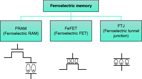
Figure 6.1 Three types of ferroelectric memories
FeFET has attracted a lot of attention for both memory and logic applications. The nonvolatile memory applications of FeFET are based on the remnant polarization in absence of an external field and the reversibility of polarization direction under an applied field. By coupling the ferroelectric polarization directly to the channel of a FET, FeFET enables a capacitor-less ferroelectric memory with simplified device design and nondestructive readout. However, analysis has also shown that FeFET retention can be degraded by the presence of a depolarization field and gate leakage [7]. The performance of FeFET is strongly affected by the interface between ferroelectric gate and semiconductor channel. Insertion of a buffer layer (e.g., high-κ), that is, a metal/ferroelectric/insulator/semiconductor, may improve the interface properties.
For stand-alone memory applications, a ferroelectric NAND (Fe-NAND) flash memory has been developed to achieve low power consumption, high reliability, and high scalability [17–21]. The Fe-NAND flash memory is composed of serially connected MFIS (Metal Ferroelectric Insulator Semiconductor) transistors.
For logic applications, it has been suggested that a FET with a ferroelectric gate stack may achieve negative capacitance and a sub-threshold slope below 60 mV/dec [12–15]. A FeFET-based SRAM with self-adjusted VTH was also developed to improve the static noise margin in a scaled SRAM with low VDD [16].
This chapter is organized in three main sections. Fe-NAND will be discussed in detail as an example of FeFET applications in standalone memory in Section 6.2. FeFET-based SRAM will be covered in Section 6.3. Section 6.4 addresses some system-level considerations with Fe-NAND memory in solid state drive (SSD) systems.
6.2 Ferroelectric FET for Flash Memory Application
Recently, SSD based on NAND flash memories was adopted in mobile and PC applications. SSD provides exceptional bandwidth, random I/O performance superior to a hard disk drive (HDD), power saving, and improved system reliability. SSD is also promising in enterprise applications including data centers [22,23]. In the last five years, as the data traffic on the internet rapidly increased, the power consumption at data centers in the United States doubled to a level corresponding to the output of five nuclear power plants. The Fe-NAND flash memory is suitable for enterprise SSD owing to its low power operation and high endurance.
The Fe-NAND flash memory is made up of serially connected MFIS, as shown in Figure 6.2a. The MFIS device in Figure 6.2b utilizes a ferroelectric SrBi2Ta2O9 (SBT) and Hf-Al-O (HAO) buffer layer in the gate stack to overcome the retention loss issues in FeFET [6]. The SBT/HAO interface is chemically stable and gate leakage is suppressed to below 1 nA/cm2. The HAO/Si interface has high quality as the channel of the transistor. Data retention is measured up to 33 days.
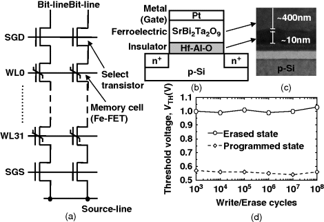
Figure 6.2 Fe-NAND flash memory [17]. (a) Fe-NAND made up of serially connected MFIS transistors. (b) MFIS transistor structure. (c) TEM cross-section of the MFIS transistor. (d) Measured programming and erasing endurance characteristics. IEEE ©. Reprinted with permission, from [19]
6.2.1 Fe-NAND Flash Memory Operation
Ferroelectric FETs are in principle scalable below 10 nm to crystal unit-cell size because data are stored in the polarization directions of a ferroelectric gate insulator. The program and erase operation conditions are illustrated in Figure 6.3c. With program/erase pulses of 6 V amplitude and 10 μs width, a 0.5 V VTH window is realized (Figure 6.3). This is significantly lower than the operation voltage of a conventional floating-gate NAND (FG-NAND) flash (∼ 20 V), which contributes to the lower operation power of Fe-NAND. Fe-NAND also achieved much longer cycling endurance, for example, 108 cycles in Figure 6.2d in comparison to ∼ 104 cycles in FG-NAND flash [17].
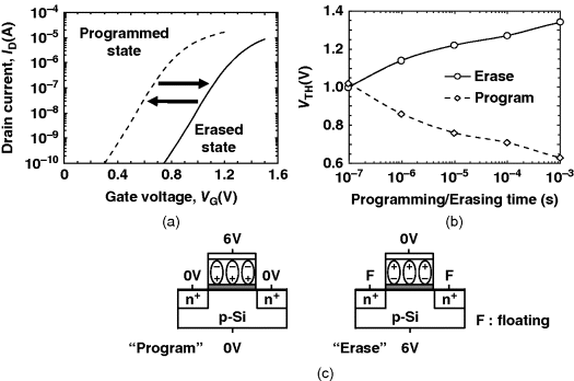
Figure 6.3 (a) Measured ID–VG characteristics after the program and erase pulse (6 V and 10 μs). (b) Measured program and erase characteristics with a 6 V pulse. (c) Bias conditions of program and erase operations of FeFET. IEEE ©. Reprinted with permission, from [19]
While the lower operation voltages of Fe-NAND helps to reduce operation power, the difference between the program voltage and the read voltage also becomes smaller and consequently read/program disturbance may increase. To reduce disturbance, a conventional NAND flash memory could adopt a negative VTH cell scheme [24], where the middle between the VTHs of erased and programmed cells is negative, as shown in Figure 6.4a. However, if the negative VTH cell scheme is applied to the Fe-NAND flash memory, the data retention drastically degrades due to the depolarization field in the ferroelectric layer. Therefore, a zero VTH memory cell scheme has been proposed for Fe-NAND flash memory to achieve both long retention and strong resistance against read/program disturbance, as shown in Figure 6.4b. By adopting this scheme, the measured VTH shift due to read disturb, program disturb, and retention loss is reduced by 32, 24 and 10%, respectively [19]. In comparison, the negative VTH cell scheme results in VTH shift as much as 192% due to retention loss. The positive VTH cell scheme, where the middle between the VTHs of erased and programmed cells is positive, suffers severe read and program disturbance.
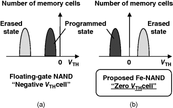
Figure 6.4 (a) Negative VTH memory cell scheme for the floating-gate NAND flash memory [24]. (b) Zero VTH memory cell scheme for the Fe-NAND flash memory. IEEE ©. Reprinted with permission, from [19]
6.2.2 Nonvolatile Page Buffer
A Fe-NAND flash memory with a nonvolatile (NV) page buffer is also proposed [18]. A critical problem of SSD is slow random write. The write unit in a NAND flash memory is a page with typical size of 4–8 KB, which is usually composed of memory cells sharing a word-line. A page is written only once to avoid a program disturb. The large page size is acceptable for digital camera, MP3 player, and camcorder application because their data size is typically over 1 MB and multiple pages are sequentially programmed. However, for a PC and data center application, the minimum write unit of the operating system (OS) is a sector of 512 Bytes. 50% of data written by OS are less than eight sectors, that is, 4 KB. A random write of data smaller than a page size frequently happens. In the case when an OS writes one sector in SSD, the remaining 80% of the page becomes garbage. As garbage accumulates, a garbage collection is performed to increase workable memory capacity. The garbage collection takes as much as 100 ms [25], which is 100 times longer than a page programming time of ∼ 800 μs and thus causes serious performance degradation. As memory cell size scales down, more cells are connected to each word-line and the page size increases, which widens the discrepancy between the page size and sector size and causes more SSD performance degradation.
To solve the random write issue, a batch write algorithm is proposed, as shown in Figure 6.5. A page buffer in the Fe-NAND flash memory temporarily stores program data. To avoid a random write, the memory programming starts only after the data to be programmed accumulate to the page size in a page buffer. In Step 1, when the OS issues one sector (512 Bytes) “write” command to the SSD, data are stored in page buffers without programming to memory cells. The NAND controller reports to the OS that the write is completed although no memory cell programming actually occurs. In Step 2, when the OS issues the second sector “write” command, the second data are also temporarily stored in the page buffer. The process continues until the data in the page buffer reach the page size (Step 3), and then memory cell programming starts in Step 4. As the logical address issued by the OS and the actually written NAND physical address are different, the NAND controller updates the logical–physical address mapping table. The batch write algorithm eliminates the data fragmentation of a page during the random write. Considering the sequential write of the SSD is over ten times faster than the random write [26], the batch write algorithm can significantly increase the SSD speed.
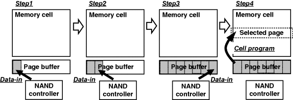
Figure 6.5 Batch write algorithm for SSD. IEEE ©. Reprinted with permission, from [18]
One problem with the batch write algorithm is data loss during a power outage. If a power outage happens in Step 4 of Figure 6.5, all data in the page buffers are lost since page buffers are volatile latch circuits. The computer system would fail because the OS recognizes that the program in steps 1–3 has been completed successfully. High reliability against a power outage is essential in an enterprise SSD. To solve this problem, a nonvolatile (NV) page buffer is proposed. The NV-page buffer consists of a volatile latch and a NV-latch, as shown in Figure 6.6. The NV-latch consists of one NMOS and one ferroelectric NMOS. The NV-latch is realized with no additional process because it has the same gate stack structure as memory cells. The area penalty for the NV-latch is less than 1% of the die size as only two transistors are added. In addition, unlike memory cells where the well is biased at 6 V, the well of the ferroelectric transistor in the NV-latch is fixed at 0 V and thus is located in the same well as the other NMOS. In normal operations, the memory cell is programmed based on data in the latch, similar to the conventional NAND flash memory. When the power outage occurs, data in the latch is transferred to the NV-latch to avoid a data loss. When power is restored, the data in the NV-latch is copied to the latch and the memory cell programming is performed based on the data in the latch. An important benefit of the Fe-NAND is that the NV-page buffer can be implemented in the peripheral circuits without any additional process cost because the Fe-FET structure is already implemented for the memory cells.
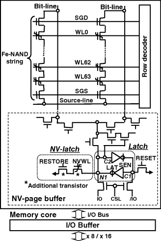
Figure 6.6 Ferroelectric NAND flash memory with nonvolatile page buffer. IEEE ©. Reprinted with permission, from [18]
6.3 Ferroelectric FET for SRAM Application
The active power consumption of digital circuits is proportional to f × C × VDD2; therefore, decreasing supply voltage (VDD) is essential for reducing the power consumption of CPU and system on chip (SoC). To realize a low voltage/power CPU and SoC, a very low supply voltage (e.g., 0.5 V) is required, which however presents a challenge for SRAM noise margin. As shown in Figure 6.7, the static noise margin (SNM) of SRAM is represented by the diagonal length of the largest square in the butterfly curves of two inverters in a SRAM cell. As VDD decreases, SNM is also reduced. At a high VDD, SNM is so large that the hold/read of the SRAM is stable. As the feature size of SRAM decreases to sub-30 nm, the VTH variation due to random dopant fluctuation (RDF) significantly increases. At VDD of 0.5 V, the SNM of conventional SRAM decreases to almost zero and the conventional SRAM can no longer operate as shown in Figure 6.7 [27]. Because decreasing VDD of SRAM is difficult in the nano-scale CMOS, the VDD of CPU and SoC cannot be further lowered.
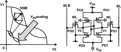
Figure 6.7 Left: Static noise margin (SNM) decreases as VDD decreases. Right: Schematic of a ferroelectric 6T-SRAM. The bodies of NMOS and PMOS are biased to VDD and VSS. The diode current to the body is suppressed at 0.5 V VDD. β ratio = 2. Since there is no extra body contact, the cell area of the ferroelectric 6T-SRAM cell is the same as the conventional 6T-SRAM. IEEE ©. Reprinted with permission, from [16]
To overcome this problem, a 6T-SRAM with Fe-FETs has been proposed [16]. It has the same structure as a conventional SRAM but uses six FeFETs instead. The Fe-FET has the same structure as the MFIS in Section 6.2 with a ferroelectric SBT layer integrated in a gate stack of standard CMOS transistors with the metal gate (Pt) and a high-κ HfAlO buffer layer between the SBT and the Si substrate.
The VTH of Fe-FETs changes by controlling the electric field between the gate and the body/channel, as shown in Figure 6.8. For example, VGB of 0.5 V applied on a NMOS forces positive polarization near the channel and decreases VTH, and a reversed VGB would increase VTH. The opposite trend VTH self-adjustment also occurs in PMOS.
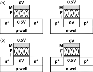
Figure 6.8 The VTH self-adjustment of pull-up and pull-down FeFETs. The electric field between the gate and channel/body shifts VTH (a) higher and (b) lower with proper bias on n-channel and p-channel FeFETs. IEEE ©. Reprinted with permission, from [16]
By biasing the bodies of the NMOS and the PMOS to VDD and VSS, respectively, the VTH of Fe-FETs automatically shifts to increase SNM. Figure 6.9 illustrates SRAM storing data “0” (a) and data “1” (b), with the directions of VTH adjustment of the pull-up and pull-down transistors marked. The VTH adjustments shift the I-V characteristics of the left and right inverters. For example, when the SRAM holds data “0,” the trip point of the right inverter decreases and that of the left inverter increases. As a result, the storage nodes V1 and V2 become more likely to hold 0 V and 0.5 V, respectively. Therefore, holding data “0” become more stable, that is, SNM is improved. A similar analysis can be done on data “1.”
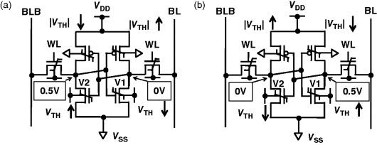
Figure 6.9 The VTH of Fe-FETs of (a) “0” datum and (b) “1” datum. The VTH automatically shifts to increase SNM. For (a) “0” datum and (b) “1” datum, the |VTH| of pull-up and pull-down FETs changes in an opposite direction to increase SNM. IEEE ©. Reprinted with permission, from [16]
Monte Carlo simulation shows 60% increase of SNM, as shown in Figure 6.10 [16]. The measured SNM on a fabricated FeFET SRAM chip is plotted in (a) for data (V1, V2) = (Low, High) and (b) for data (V1, V2) = (High, Low). A large SNM of 1.46 V is demonstrated, which is even larger than the 1.27 V SNM of an ideal inverter with infinitely steep slope [16].
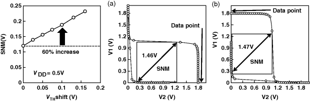
Figure 6.10 Simulated read SNM without the VTH variation. SNM increases by 60% from 0.11 V of the conventional SRAM to 0.19 V with 0.1 V VTH shift. Measured SNM for (a) data (V1, V2) = (Low, High) and (b) data (V1, V2) = (High, Low). IEEE ©. Reprinted with permission, from [16]
The on-current of the read NMOS determines the read speed. During the read operation, the VTH of the read transistor is automatically set to the low value. As a result, the read cell current increases to enhance the read speed, as shown in Figure 6.11.
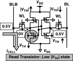
Figure 6.11 High-speed read. The VTH of the read NMOS is automatically set low to increase current for high speed reading. IEEE ©. Reprinted with permission, from [16]
The sub-threshold current of the off-state FETs shown in Figure 6.12 determines the leakage of the SRAM cell. During the stand-by operation, the VTH of these transistors is automatically set to high values to reduce leakage current. Leakage reduction of 42% is demonstrated by measurement [16].
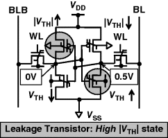
Figure 6.12 Stand-by leakage current reduction. The |VTH| of both leakage NMOS and PMOS is automatically set to high, suppressing the leakage current. IEEE ©. Reprinted with permission, from [16]
The enlarged SNM in the ferroelectric SRAM realizes the VDD scaling of 0.11 V and decreases the active power by 32% [16]. Since the transistor count is minimized to six, similar to a conventional SRAM, the ferroelectric SRAM cell also achieves the smallest cell size.
6.4 System Consideration: SSD System with Fe-NAND Flash Memory
The write speed in SSD can be enhanced by increasing the number of NAND chips (NNAND) written in parallel; however, NNAND is limited by the chip power consumption in the given SSD power budget because current is also increased in proportion to NNAND [23]. Therefore, minimizing NAND power consumption is essential for realizing high-speed SSD. As the feature size of NAND flash memory decreases, the total bit-line capacitance increases and contributes significantly to the power consumption. The best strategy to decrease power consumption is by reducing VCC. However, in conventional FG-NAND, decreasing VCC below 2 V results in an increasing total power consumption because more charge pump stages are needed (to boost VCC to 20 V for programming). Increasing power consumed by charge pumps surpasses the power saving by lowering VCC.
Fe-NAND can be programmed with a much lower voltage, which helps to suppress the power consumption of the charge pump. As shown in Figure 6.13, NNAND of the Fe-NAND is maximized around VCC = 1.0 V. Higher VCC increases the bit-line charging current and the total power consumption, which results in lower NNAND under power constraint. Lower VCC increases the required charge pump stages and the total power consumption, which also reduces NNAND. The optimal NNAND of the Fe-NAND is 6.9 times higher than that of the FG-NAND. Notice that the NNAND of FG-NAND optimizes at higher VCC because of the higher programming voltage of FG-NAND.
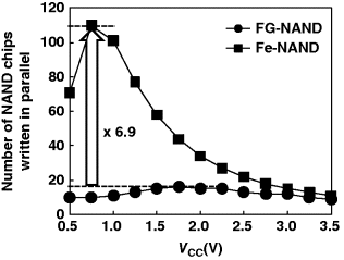
Figure 6.13 Number of NAND chips written in parallel (NNAND) as a function of VCC. The 6.9 times higher write performance is obtained in the Fe-NAND at VCC = 1.0 V. IEEE ©. Reprinted with permission, from [28]
The improved NNAND in FeNAND translates directly into a better performance of the FeNAND-based SSD. As shown in Figure 6.14, Fe-NAND Flash SSD achieves a throughput of 9.5 GB/s at VCC = 1.0 V, significantly higher than that of FG-NAND SSD (below 2 GB/s).
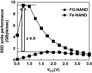
Figure 6.14 SSD write performance of the FG-NAND and the Fe-NAND. The Fe-NAND can achieve 9.5 GB/s at VCC = 1.0 V which is 6.9 times higher than the FG-NAND at VCC = 1.8 V. IEEE ©. Reprinted with permission, from [28]
6.5 Perspectives and Summary
FeFET has demonstrated promising potential for both standalone flash memory applications and embedded logic/SRAM applications. The Fe-NAND flash memory discussed in this chapter achieves a much lower operation voltage (∼ 6 V) than that of conventional FG-NAND (∼ 20 V), which not only reduces power consumption but also improves reliability (from 104 to 108 cycles). For SRAM/logic applications, the ferroelectric SRAM has a unique configuration to adjust VTH by biasing the bodies of NMOS and PMOS to VDD and VSS. During the read and the hold, the VTH of Fe-FETs automatically changes to increase SNM by 60%. In the standby mode, the VTH of the FeFET SRAM cell increases to decrease the leakage current by 42%. During reading, the VTH of the read transistor decreases to increase the cell read current for a fast reading speed. During writing, the VTH of the SRAM cell dynamically changes and assists the cell data to flip. The enlarged SNM enables VDD reduction by 0.11 V, which decreases the active power by 32%. The ferroelectric SRAM also minimizes footprint.
SSD based on Fe-NAND benefits significantly from the low operation voltage of Fe-NAND. A lower supply voltage can be used without incurring higher power consumption from charge pumps. The 86% power reduction in Fe-NAND increases the number of NAND chips written in parallel in SSD by 6.9 times and enhances the SSD performance up to 9.5 GB/s.
The performance of FeFET devices and systems hinges on high-quality materials and integration technologies. The SBT/HAO gate stack utilized in the MFIS and ferroelectric SRAM structures in this chapter plays a critical role to enable functional FeFETs with good data retention. Integration of ferroelectric materials in a standard CMOS process has always been a challenge. A recent discovery of ferroelectric property in Si-doped HfO2 allows fabrication of FeFETs at a highly scaled node in the state of the art CMOS process [30]. A 28 nm FeFET with TiN/Si:HfO2/SiO2/Si gate stack has been demonstrated [31]. A 0.9 V memory window was achieved with ±5 V 20 ns program/erase pulses. This fabrication-friendly material may provide a promising solution for ferroelectric devices including FeFET.
Table 6.1 summarizes some key parameters of FeFET memories reported in the literature.
Table 6.1 Summary of key FeFET memory parameters
| Parameter | Value | |
| Device structure | 1-Transistor (1 T) | |
| Feature size F | Demonstrated | 28 nm [31] |
| Projected | The same as CMOS transistor | |
| Cell size | Demonstrated | 4F2 [32] |
| Projected | 4F2 | |
| W/E speed | Demonstrated | 10 ns [33] |
| Projected | Ferroelectric switching time<100 ps | |
| W/E operation voltage | Demonstrated | ±5 V (20 ns pulse) [31] |
| Projected | — | |
| Write energy per bit | Demonstrated | 1 fJ [34] |
| Projected | 0.1 fJ | |
| Cycling endurance | Demonstrated | 1012 [6] |
| Projected | > 1012 | |
| Retention | Demonstrated | 33 d [35] |
| Projected | > 10 yr |
References
- 1. Scott, J.F. and De Araujo, C.A.P. (1989) Ferroelectric memories. Science, 246, 1400–1405.
- 2. Chung, Y. (2002) Experimental 128-kbit ferroelectric memory with 1012 endurance and 10-year data retention. IEE Proceedings-Circuits Devices and Systems, 149(2), 136–142.
- 3. Kang, Y.M. et al. (2006) World smallest 0.34 μm2 COB cell 1T1C 64Mb FRAM with new sensing architecture and highly reliable MOCVD PZT integration technology, Symp. VLSI Tech., pp. 124–125 Jun.
- 4. Heyman, P.M. and Heilmeier, G.H. (1966) A ferroelectric field effect device. Proceedings of IEEE, 54(6), 842–848.
- 5. Wu, S.Y. (1974) A new ferroelectric memory device, metal–ferroelectric–semiconductor transistor. IEEE Transactions on Electron Devices, ED-21(8), 499–504.
- 6. Sakai, S. and Ilangovan, R. (2004) Metal–ferroelectric–insulator–semiconductor memory FET with long retention and high endurance. IEEE Electron Device Letters, 25(6), 369–371.
- 7. Ma, T.P. and Han, J.P. (2002) Why is nonvolatile ferroelectric memory field-effect transistor still elusive? IEEE Electron Device Letters, 23(7), 286–388.
- 8. Hoffman, J., Pan, X., Reiner, J.W., Walker, F.J., Han, J.P., Ahn, C.H., and Ma, T.P. (2010) Ferroelectric field effect transistors for memory applications. Advanced Materials, 22, 2957–2961.
- 9. Kaneko, Y., Tanaka, H., Ueda, M., Kato, Y., and Fujii, E. (2011) A dual-channel ferroelectric-gate field-effect transistor enabling NAND-type memory characteristics. IEEE Transactions on Electron Devices, 58(5), 1311–1318.
- 10. Tsymbal, E.Y. and Kohlstedt, H. (2006) Tunneling across a ferroelectric. Science, 313(5784), 181–183.
- 11. Chanthbouala, A. et al. (2012) Solid-state memories based on ferroelectric tunnel junctions. Nature Nanotechnology, 7, 101–104.
- 12. Salahuddin, S. and Datta, S. (2008) Use of negative capacitance to provide voltage amplification for low power nanoscale devices. Nano Letters, 8(2), 405–410.
- 13. Salvatore, G.A., Bouvet, D., and Ionescu, A.M. (Dec. 2008) Demonstration of subthrehold swing smaller than 60mV/decade in Fe-FET with P(VDF-TrFE)/SiO2 gate stack, IEDM Tech. Dig.
- 14. Rusu, A., Salvatore, G.A., Jimenez, D., and Ionescu, A.M. (Dec. 2010) Metal-ferroelectric-metal-oxide-semiconductor field effect transistor with sub-60mV/decade subthreshold swing and internal voltage amplification, IEDM Tech. Dig., pp. 395–398.
- 15. Bratkovsky, M. and Levanyuk, A.P. (2006) Depolarizing field and “real” hysteresis loops in nanometer-scale ferroelectric films. Applied Physics Letters, 89(25), 253108-1-3
- 16. Tanakamaru, S., Hatanaka, T., Yajima, R., Takahashi, M., Sakai, S., and Takeuchi, K. (Dec. 2009) A 0.5 V operation, 32% lower active power, 42% lower leakage current, ferroelectric 6T-SRAM with VTH self-adjusting function for 60% larger static noise margin, IEDM Tech. Dig., pp. 283–286.
- 17. Sakai, S., Takahashi, M., Takeuchi, K., Li, Q.H., Horiuchi, T., Wang, S., Yun, K.Y., Takamiya, M., and Sakurai, T. (May. 2008) Highly Scalable Fe(Ferroelectric)-NAND Cell with MFIS(Metal-Ferroelectric-Insulator-Semiconductor) Structure for Sub-10nm Tera-Bit Capacity NAND Flash Memories, Non-Volatile Semiconductor Memory Workshop (NVSMW), pp. 103–104.
- 18. Hatanaka, T., Yajima, R., Horiuchi, T., Wang, S., Zhang, X., Takahashi, M., Sakai, S., and Takeuchi, K. (2010) Ferroelectric(Fe)-NAND flash memory with batch write algorithm and smart data store to the nonvolatile page buffer for data center application high-speed and highly reliable enterprise solid-state drives. IEEE J. Solid-State Circ., 45(10), 2156–2164.
- 19. Hatanaka, T., Takahashi, M., Sakai, S., and Takeuchi, K. (Sep. 2009) A zero VTH memory cell ferroelectric-NAND flash memory with 32% read disturb, 24% program disturb, 10% data retention improvement for enterprise SSD, European Solid-State Device Research Conference (ESSDERC), pp. 225–228.
- 20. Yajima, R., Hatanaka, T., Takahashi, M., Sakai, S., and Takeuchi, K. (Oct. 2009) A Negative Word-line Voltage Step-Down Erase Pulse Scheme with ΔVTH = 1/6 ΔVERASE for Enterprise SSD Application Ferroelectric(Fe)-NAND Flash Memories, Inter. Conf. Solid State Dev. and Mater. (SSDM).
- 21. Noda, S., Hatanaka, T., Takahashi, M., Sakai, S., and Takeuchi, K. (Oct. 2009) A 1.2V Operation 2.43 Times Higher Power Efficiency Adaptive Charge Pump Circuit with Optimized VTH at Each Pump Stage for Ferroelectric (Fe)-NAND Flash Memories Inter. Conf. Solid State Dev. and Mater. (SSDM).
- 22. Takeuchi, K. (2008) NAND Memories for SSD IEEE Inter. Solid-State Circ. Conf. (ISSCC), Tutorial T7 Feb.
- 23. Takeuchi, K. (Jun. 2008) Novel co-design of NAND flash memory and NAND flash controller circuits for sub-30nm low-power high-speed solid-state drives (SSD), Symposium on VLSI Circuits, pp. 124–125.
- 24. Takeuchi, K., Satoh, S., Tanaka, T., Imamiya, K., and Sakui, K. (1999) A negative Vth cell architecture for highly scalable, excellently noise-immune, and highly reliable NAND flash memories. Journal of Solid State Circuits, 34(5), 675–684.
- 25. Takeuchi, K. et al. (Feb. 2006) A 56nm CMOS 99mm2 8Gb multi-level NAND flash memory with 10MB/s program throughput, IEEE Inter. Solid-State Circ. Conf. (ISSCC) pp. 144–145.
- 26. Agrawal, N., Prabhakaran, V., Wobber, T.d., Davis, J.D., Manasse, M., and Panigrahy, R. (2008) Design Tradeoffs for SSD Performance, USENIX Technical Conference.
- 27. Itoh, K. (Feb. 2009) Adaptive Circuits for the 0.5-V Nanoscale CMOS Era, ISSCC, pp. 14–20.
- 28. Miyaji, K., Noda, S., Hatanaka, T., Takahashi, M., Sakai, S., and Takeuchi, K. (2010) A 1.0 V Power Supply, 9.5 GByte/sec Write Speed, Single-Cell Self-Boost Program Scheme for Ferroelectric NAND Flash SSD, IEEE International Memory Workshop, pp. 42–45.
- 29. Miyaji, K., Noda, S., Hatanaka, T., Takahashi, M., Sakai, S., and Takeuchi, K. (2011) A 1.0 V power supply, 9.5 GByte/sec write speed, single-cell self-boost program scheme for ferroelectric NAND flash SSD. Solid-State Electronics, 58(1), 34–41.
- 30. Böscke, T.S., Müller, J., Bräuhaus, D., Schröder, U., and Böttger, U. (Dec. 2011) Ferroelectricity in hafnium oxide: CMOS compatible ferroelectric field effect transistors, IEDM Tech. Dig., pp. 547–550.
- 31. Müller, J. et al. (Jun. 2012) Ferroelectricity in HfO2 enables nonvolatile data storage in 28 nm HKMG, Symp. on VLSI Tech., pp. 25–26.
- 32. Zhang, X., Takahashi, M., Takeuchi, K., and Sakai, S. (2011) First 64 kb ferroelectric-NAND flash memory array with 7.5 V program, 108 endurance and long data retention, Inter. Conf. Solid State Dev. and Mater. (SSDM), pp. 975–976.
- 33. Kaneko, Y., Nishitani, Y., Ueda, M., Tokumitsu, E., and Fujii, E. (2011) A 60nm channel length ferroelectric-gate field-effect transistor capable of fast switching and multilevel programming. Applied Physics Letters, 99(18), 182902 1-3.
- 34. Fu, W., Xu, Z., Bai, X., Gu, C., and Wang, E. (2009) Intrinsic memory function of carbon nanotube-based ferroelectric field-effect transistor. Nano Letters, 9(3), 921–925.
- 35. Takahashi, M. and Sakai, S. (2005) Self-aligned-gate metal/ferroelectric/insulator/semiconductor field-effect transistors with long memory retention. Japanese Journal of Applied Physics, 44(25), L800–L802.