
14
Re-Invention of FET
Toshiro Hiramoto
Institute of Industrial Science, The University of Tokyo, Japan
14.1 Introduction
The silicon metal oxide semiconductor field effect transistor (MOSFET) for very large scale integration (VLSI) has been scaled down for more than 40 years in order to attain higher speed, lower power, higher integration, and lower cost. The gate length has reached as small as 20 nm and more than a billion transistors are now integrated in a single chip. The silicon devices are certainly in both the nanometer regime and the giga-scale integration regime. It is predicted in the 2011 version of the International Technology Roadmap for Semiconductors (ITRS) [1] that FET will continue to miniaturize and its gate length will become less than 10 nm in 2022 in production. The semiconductor technologies will continue to be the basis of the contemporary information-oriented society.
However, there are a lot of technical barriers to realize such small and giga-scale devices with higher performance and lower power dissipation. It is now well recognized that simple scaling of conventional bulk MOSFETs will fail in the nanometer regime. Therefore, nonconventional MOSFETs with new transistor structures and/or new channel materials have been under development and even re-invention of new types of FETs has been pursued at research level.
In this chapter, the historical trend of MOSFETs in the past and the future trend predicted by ITRS are compared first in order to look into the technological barriers that should be targeted. Next, the present status of the development of nonconventional devices with new structures and new materials are briefly mentioned as near-term solutions. Then, completely new types of transistors that have been re-invented recently are described in detail.
14.2 Historical and Future Trend of MOSFETs
Figure 14.1 shows the historical and future trends of the speed and energy dissipation of MOSFETs. In this figure, CV/I is used as a figure of merit for evaluating the circuit speed that is a reciprocal of the circuit delay, where C is the gate capacitance (other load capacitances are ignored for simplicity), V is the supply voltage, and I is the on-current of MOSFETs. Similarly, CV2 is used as a figure of merit for evaluating energy dissipation. It is assumed that Wg = 3Lg, where Wg is the gate width and Lg is the gate length. Please note that CV2 represents active energy dissipation only and does not include static energy dissipation. Data up to 2011 were taken from the typical device parameters presented at the International Electron Devices Meeting (IEDM), and data after 2011 are based on ITRS prediction for high performance (HP) devices and III-V multigate (MG) devices [1].
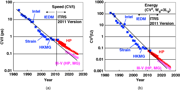
Figure 14.1 Historical and future trends of (a) the speed and (b) the energy dissipation of MOSFETs. The data up to 2011 were taken from typical device parameters presented in IEDM and the data after 2011 are based on ITRS prediction for HP and III-V MG devices
It is clearly seen that both circuit delay and energy decreased rapidly until the mid2000s. However, advancement has started saturating since then. In the ITRS prediction, advancement will continue, but the trends of delay and energy advancement will slow down. Speed and energy will be much better when MG devices are realized with III-V channel materials, which have higher mobility than silicon. Therefore, the development of high mobility channel transistors is certainly necessary.
In order to look into these trends in more detail, the historical and future trends of supply voltage (Vdd) and on-current (Ion) are summarized in Figure 14.2, and Lg and equivalent oxide thickness (EOT) are shown in Figure 14.3.
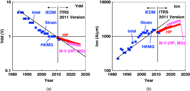
Figure 14.2 Historical and future trends of (a) Vdd and (b) Ion
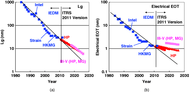
Figure 14.3 Historical and future trends of (a) Lg and (b) EOT
It is found that Vdd, Ion, Lg, and EOT show similar behavior: rapid advancement until mid 2000s but saturating since then, indicating that device technology has faced severe technical barriers. Figures 14.2 and 14.3 indicate the years when strain technology [2] and high k metal gate (HKMG) [3] were first introduced. These technologies certainly contributed to the device advancement (especially, HKMG contributed largely to the EOT reduction), but it is surprising to know that the advancements by these technologies were only temporary. In the prediction by ITRS, III-V devices will have much higher Ion while keeping EOT relatively thicker than silicon HP transistors, contributing largely to higher speed and lower energy.
The off current (Ioff) is plotted in Figure 14.4a. Ioff exponentially increased until the mid2000s and completely stopped increasing since then. This means that Ioff had reached the highest limit for HP transistors, indicating that threshold voltage (Vth) has not been reduced since then. Apparently, one of the reasons for the saturation of transistor speed, energy, Vdd, and Ion after the mid2000s in Figures 14.1 and 14.2 is that Vth had to remain almost constant and overdrive voltage (Vdd – Vth) rapidly decreased as Vdd decreased. Therefore, new device technology that has high overdrive voltage at a constant Ioff is strongly required.

Figure 14.4 Historical and future trends of (a) Ioff and (b) M1 pitch
On the other hand, the M1 pitch is plotted in Figure 14.4b. The M1 pitch has been continuously reduced unlike Lg and will be reduced in a similar rate in the prediction. The M1 pitch directly corresponds to the transistor integration level, which will not lose pace because the M1 pitch is purely determined by the lithography and is almost independent of the technological barriers for transistor speed and energy.
14.3 Near-term Solutions
Considering the historical trend and future trend in Figures 14.1–14.4, a schematic of device characteristics that should be targeted is illustrated in Figure 14.5.
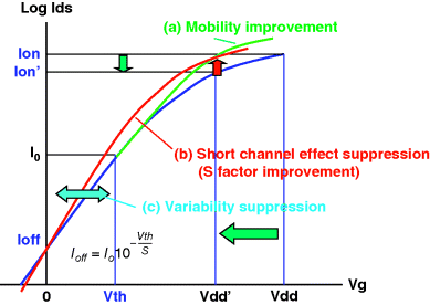
Figure 14.5 Schematic of device characteristics that should be targeted
14.3.1 High Mobility Channel Transistor
First, in order to attain higher Ion at constant Ioff at lower Vdd, the mobility improvement of channel material is certainly necessary. The characteristics of a high mobility channel transistor are schematically shown in Figure 14.5a, comparing with a conventional silicon channel bulk transistor. Thanks to high mobility, a higher Ion can be obtained with a given overdrive voltage, or the same Ion can be obtained with reduced overdrive voltage, than with a conventional device.
Generally, III-V compound semiconductors, including GaAs, InP, InAs, InSb, and their ternary or quaternary alloy semiconductors, have much higher electron mobility than silicon, and they are promising materials for n-type FETs. On the other hand, Ge and SiGe have higher hole mobility than silicon and they are attractive for p-type FETs. High mobility transistors using III-V or Ge have been widely studied, and the integration of III-V nFETs and Ge pFETs in a chip has been also achieved at research level [4], as shown in Figure 14.6. Moreover, a Ge nFET, which has higher electron mobility than silicon, and a III-V pFET, whose hole mobility is enhanced by strain, are also being studied.
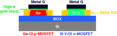
Figure 14.6 Schematic of the integration of III-V nFETs and Ge pFETs in a chip [4]
14.3.2 Multi-gate Transistor
Second, in order to attain lower Vth at constant Ioff, the steep subthreshold slope is necessary. The subthreshold properties are generally characterized by the subthreshold gate voltage swing to achieve 10× drain current change (Subthreshold swing, SS). It is well known that the minimum SS is kT/q as long as the operation principle is based on conventional FET, where k is the Boltzmann constant, T the temperature, and q the elementary charge. The minimum SS at room temperature is 60 mV/dec. In conventional bulk transistors, the SS is degraded due to the short channel effect and the typical value of SS is approximately 100 mV/dec. The ideal subthreshold characteristics with SS = 60 mV/dec are schematically shown in Figure 14.5b, compared with conventional single-gate bulk transistors. A higher Ion can be obtained with a given Ioff and Vdd, or the same Ion can be obtained with a reduced Vdd, than with conventional devices.
The subthreshold characteristics close to the ideal SS can be obtained by better electrostatic control by gate electrode, which can be achieved by changing the transistor structure. Figure 14.7 shows the evolution of transistor structure from single-gate structure to three-dimensional (3D) multi-gate structures. The FinFET is one of the double-gate structures. In a tri-gate transistor, three surfaces of the channel are surrounded by the gate electrodes. The ideal structure in terms of the electrostatic control by gate is the gate all around (GAA) nanowire structure [5].
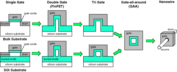
Figure 14.7 Evolution of transistor structure from single-gate to 3D MG structures
The tri-gate transistor has been in production, where the short channel effect is well suppressed and SS of approximately 70 mV/dec has been attained in transistors with Lg as small as 30 nm [6], as shown in Figure 14.8. The data for a tri-gate transistor in the year 2011are also plotted in Figures 14.1–14.4. Thanks to better SS, Vdd can be reduced to 0.8 V, leading to an improvement of the energy, as shown in Figure 14.1b.
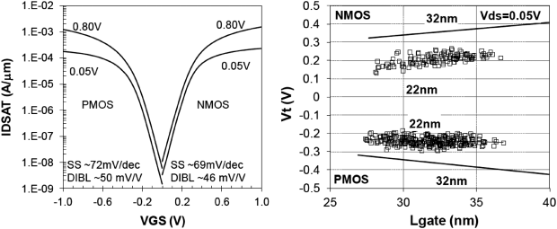
Figure 14.8 Subthreshold characteristics and short channel behavior of tri-gate FETs [6]. © 2012 IEEE
14.3.3 Intrinsic Channel Transistor
Third, in order to suppress the characteristic variability, intrinsic channel transistors should be realized. One of the main obstacles that prevent further device scaling and Vdd lowering is the random variability of transistor characteristics, which is not represented in Figures 14.1–14.4. It is known that the main origin of random variability in conventional bulk transistors is random dopant fluctuation (RDF) [7]. Since the number and the position of dopant atoms in the transistor channel are randomly distributed, Vth of each transistor also varies randomly. It is experimentally confirmed that Vth of bulk transistor follows a normal distribution up to ±5σ [8].
The only way to suppress the variability due to RDF is to eliminate dopant atoms from the transistor channel, which is impossible in conventional bulk planar transistors because a heavily doped channel is necessary to suppress the short channel effect. The intrinsic channel or very lightly doped channel, whose channel is fully depleted (FD), can be realized using a silicon on insulator (SOI) transistor or a 3D multi-gate transistor, where the short channel effect is well suppressed not by a heavily doped channel but by better gate electrostatic control.
Figure 14.9 compares measured characteristics variability in 1 k bulk transistors and 1 k intrinsic channel FD SOI transistors fabricated using 65 nm technology [9]. Compared to bulk transistors, the intrinsic channel FD SOI transistors have much smaller random Vth variability. On-current (Ion) variability at Vgs = Vds = 1.2 V is also suppressed in the intrinsic channel transistors. The intrinsic channel is a very effective way to suppress random variability.
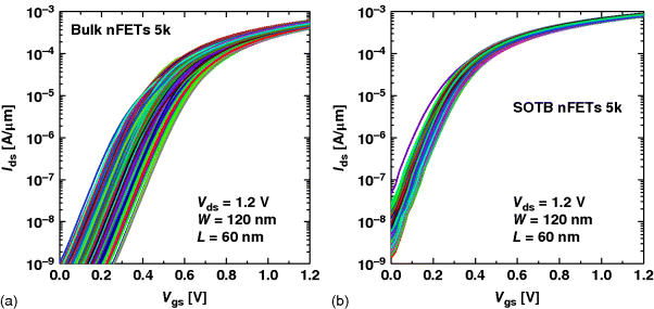
Figure 14.9 Characteristics of (a) 1 k bulk and (b) 1 k intrinsic channel FD SOI transistors [9]
However, intrinsic channel transistors still have random variability, which may be caused by other origins than RDF, including random variations of gate work function. As the transistor size shrinks and the integration level increases, the variability problem becomes more severe. Any possible origins of variability should be strictly suppressed in nanometer and giga-scale transistors.
The variability problem will also arise in any of the new types of devices that will be introduced in the following sections. The origins of variability in devices with new operation principles may be different from conventional FETs. The variability problem should be primarily considered in the exploration of new types of devices for VLSI applications.
14.4 Long-term Solutions
14.4.1 Energy Efficiency
Before discussing new types of devices as long-term solutions, the energy efficiency of CMOS logic circuits are reconsidered in this subsection. Figure 14.10 shows calculated delay, power, and energy of a CMOS logic circuit [10] as a function of Vdd, where parameters of the 65 nm technology generation are assumed, both active and static power dissipations are considered, and the energy is defined as the product of power and delay. As Vdd is reduced, the delay increases, while the power dissipation dramatically decreases. Here, we should pay attention to the energy, which has the optimum (minimum) value (Eopt) at a certain Vdd. The energy decreases as Vdd decreases due to the reduction of active energy, while the energy increases as Vdd is further reduced due to the increase in the static energy. Vopt is defined as Vdd at which the energy becomes optimum. Since the operation at Vopt can achieve the most energy efficiency, Vopt is the target supply voltage for ultra-low power and energy efficient applications [10].
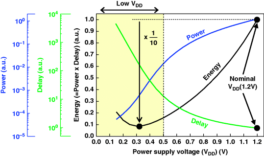
Figure 14.10 Calculated delay, power, and energy of a CMOS logic circuit assuming 65 nm CMOS process as a function of Vdd [10]
Figure 14.11 shows energy versus Vdd assuming various subthreshold swings (SS). In the calculation, Ioff at Vds = Vdd is fixed. It should be noted that the energy dissipation strongly depends on SS, and both Eopt and Vopt drastically decreases as SS decreases. The ideal ultra-low energy circuits cannot be achieved by conventional CMOS devices whose SS is more than 60 mV/dec. This is a strong motivation for the invention of new types of FETs that have steeper subthreshold swing less than 60 mV/dec.
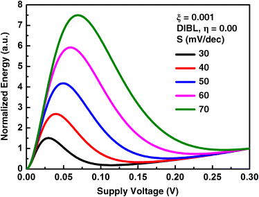
Figure 14.11 Calculated energy as a function of Vdd at various SS [11]
14.4.2 Impact-ionization MOS
One of the early attempts to pursue steep subthreshold device was impact-ionization MOS (I-MOS) [12]. The I-MOS is in the form of a gated p-i-n structure and uses a gain mechanism caused by the modulation of impact-ionization related breakdown voltage. Since the impact-ionization is an abrupt function of the electric field, the device has a subthreshold slope much lower than kT/q.
Figure 14.12a shows a schematic n-channel device structure [12]. The main differences between I-MOS and a conventional n-channel MOSFET are an n-type source and an offset between source and gate in I-MOS. Figure 14.12b shows experimental I-V characteristics of silicon-based p-channel I-MOS [12]. Extremely steep subthreshold swing (∼10 mV/dec) is achieved. One of the drawbacks of I-MOS is that the device inherently requires high drain voltage to give rise to the breakdown. The channel material should have a narrow bandgap to realize low voltage operation. Another concern of I-MOS is the delay associated with positive feedback that is intrinsic to impact ionization phenomena.
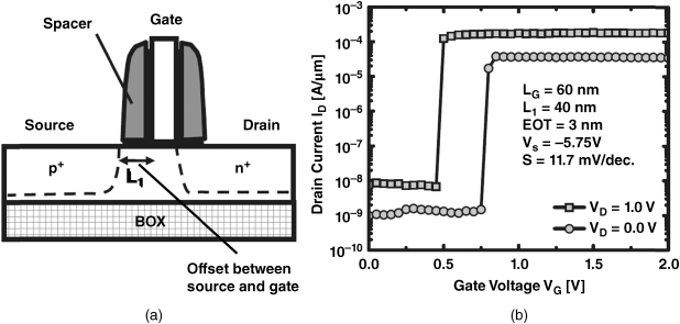
Figure 14.12 Impact-ionization MOS (I-MOS). (a) A schematic n-channel device structure. (b) Experimental result of silicon p-channel I-MOS showing very steep subthreshold swing [12]
14.4.3 Tunnel FET
One of the most promising and most actively researched steep SS devices is the tunnel FET (TFET). TFETs make use of tunneling current instead of diffusion to avoid the limitation by kT/q in the subthreshold region. Figure 14.13 shows a schematic device structure and band diagram of an n-channel TFET that consists of p+ source, n+ drain, and gate [13]. When the gate voltage is 0 V, the channel is fully depleted and the device is in the OFF state (Figure 14.13b). When the positive gate voltage is applied, the device turns on by the Zener tunneling (Figure 14.13c). Since the Fermi tail is cutoff by the bandgap the subthreshold swing is not limited to kT/q and the off-current can be significantly below that of the conventional MOSFET [13]. Detailed operation principles of TFETs are found in review papers [13,14].
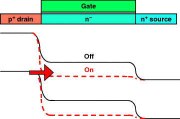
Figure 14.13 Schematic structure and band diagram of a n-channel tunnel FET showing the operation principle [13]. (a) A simple pn junction without the gate. (b) A tunnel FET with gate in OFF state. (c) A tunnel FET with gate in ON state
TFETs have been fabricated and a sub-60 mV/dec subthreshold slope has been observed in various channel materials including Si, Ge, and III-V semiconductors. Figure 14.14a shows an example of a silicon TFET [15]. The minimum SS of 36 mV/dec is obtained, although this small SS is achieved in only narrow Ids range (approximately one order) and at very small Ids (Ids ∼ 1 pA/μm). The average SS in three orders of magnitude of Ids is 81 mV/dec, that is larger than the ideal SS in conventional MOSFETs.
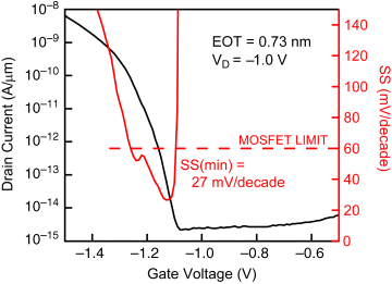
Figure 14.14 Examples of I-V characteristics of TFETs. (a) S silicon TFET [15]. SS of 36 mV/dec is observed only in very narrow Ids range. (b) A heterojunction InGaAs TFET compared with a thin body InGaAs MOSFET [16]
Figure 14.14b shows another example of a TFET composed of heterojunction InGaAs, compared with a thin body InGaAs MOSFET at matched Ioff = 200 pA, Lg = 150 nm, EOT = 1.15 nm, and Vds = 0.3 V [16]. SS of the InGaAs TFET is smaller than 60 mV/dec in the range from 3 × 10⁻¹⁰ to 3 × 10⁻⁹ A. Due to the steeper SS, the InGaAs TFET shows gain over the InGaAs MOSFET at low overdrive, but Ion is much smaller at Vgs – Vth ∼ 0.6 V. The smaller Ion is a significant disadvantage of TFETs.
Figure 14.15a shows an example of sub-60 mV/dec characteristics of an InAs/Si heterojunction p-channel TFET [17]. Excellent SS of 21 mV/dec is achieved in a wide Id range of four orders of magnitude. The on/off ratio reaches approximately 106. However, this InAs/Si heterojunction p-channel TFET has another disadvantage. Figure 14.15b shows another example of an InAs/Si heterojunction p-channel TFET showing I-V characteristics with various drain voltage (Vds) dependence [17]. It is found that Vth decreases as Vds increases. In conventional MOSFETs, this phenomenon of Vds dependence of Vth is known as drain induced barrier lowering (DIBL) and characterized by η = |ΔVth/ΔVds|. Although the mechanism may be different in TFETs, some TFETs show very high η, especially heterojunction TFETs. η reaches as large as 0.74 in Figure 14.15b [17].
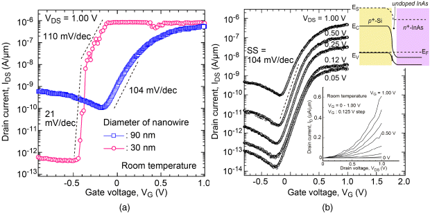
Figure 14.15 I-V characteristics of InAs/Si heterojunction TFETs [17]. (a) Excellent SS of 21 mV/dec is achieved. (b) Large Vds dependence of Vth is observed
In order to investigate the effect of η in steep subthreshold devices, the energy dissipation is calculated at fixed SS of 30 mV/dec at various η, as shown in Figure 14.16 [11]. Ioff at Vds = Vdd is fixed in the calculation, and hence Vth increases as Vds decreases in high η devices. As η increases, the energy as well as Vopt and Eopt increases. This is because delay increases due to increases Vth at low Vdd. This result indicated that the advantage of steep SS is offset by large η. Therefore, η (Vds dependence of Vth) should be suppressed in steep subthreshold devices.
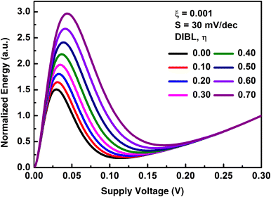
Figure 14.16 Calculated energy as a function of Vdd with fixed SS of 30 mV/dec at various η (= |ΔVth/ΔVds|) [11]
14.4.4 Negative Capacitance FET
SS is given by [18]
where Vg is the gate voltage, Ψs is the surface potential, Cs is the semiconductor capacitance, Cins is the gate insulator capacitance, and Id is the drain current. The term ![]() is the body factor and is often called the m-factor, while the term
is the body factor and is often called the m-factor, while the term ![]() is called the n-factor. It is the n-factor that is limited by kT/q due to the carrier injection in the source. The I-MOS and tunnel FETs in the previous subsections achieve SS of less than 60 mV/dec by modifying the n-factor. If the m-factor can be less than unity, the device with less than 60 mV/dec is also achievable. The negative gate insulator capacitance makes it possible.
is called the n-factor. It is the n-factor that is limited by kT/q due to the carrier injection in the source. The I-MOS and tunnel FETs in the previous subsections achieve SS of less than 60 mV/dec by modifying the n-factor. If the m-factor can be less than unity, the device with less than 60 mV/dec is also achievable. The negative gate insulator capacitance makes it possible.
Figure 14.17 shows a schematic of a negative capacitance FET and equivalent gate capacitance circuit [18]. The gate stack has a thin ferroelectric layer, which can introduce a positive feedback on the charge that causes polarization and amplifies the gate voltage, resulting in an m-factor of less than unity. Figure 14.18 shows measured device characteristics at room temperature [19]. SS of less than 60 mV/dec is obtained in a wide range of drain currents.
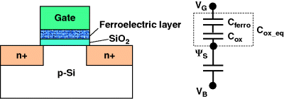
Figure 14.17 A schematic and equivalent gate capacitance circuit in the negative capacitance FET with a thin ferroelectric layer [16]
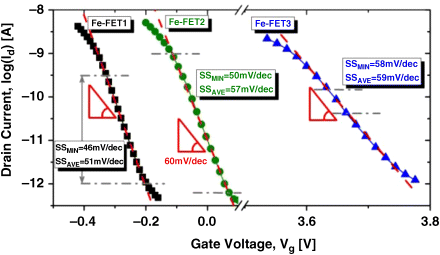
Figure 14.18 Measured I-V characteristics of negative capacitance FETs at room temperature [17]. © 2010 IEEE
However, the average SS obtained is not small enough and the on-current is still very low for practical use. The main challenge of the negative capacitance FET is the selection of gate stack materials that can provide much smaller average SS and higher on-current. The threshold voltage adjustments, integration of nFET and pFET, and the stability, reliability, and variability will be also critical issues.
14.4.5 MEMS Switch
Another approach to attain super steep subthreshold characteristics is to utilize a micro-electro-mechanical system (MEMS). The movement of a MEMS structure is affected by both elastic and electrostatic forces, and the structure suddenly moves when the balance between these forces is broken.
Figure 14.19 shows an example of a MOSFET with the MEMS structure. The device has a movable gate electrode that is fabricated by MEMS technology and suspended above the channel [20]. When the gate voltage (Vgs) is 0 V, the gate is located far above the gate and is not in contact with the gate oxide. Then, the inversion layer is not formed in the channel and hence, the device is in the OFF state (Figure 14.19a). When Vgs increases, a downward electrostatic force applied to the movable gate increases, and the movable gate is suddenly pulled down to the gate oxide at a certain voltage of Vgs, as shown in Figure 14.19b. This voltage is called the “pull-in” voltage (Vpull-in).

Figure 14.19 Schematics of an MOSFET with a movable gate electrode [18]. (a) OFF state at Vgs = 0 V. This state is called “pull-out.” (b) ON state at sufficiently large Vgs. The gate electrode is pulled in and the device is at ON state
Figure 14.20 shows measured I-V characteristics of a MOSFET with a movable gate [20]. In this specific device, an additional lower gate electrode is formed in the vicinity of the channel to control Vpull-in of the device. When Vgs increases, drain current rapidly increases at a certain Vgs. This voltage is Vpull-in and the subthreshold slope is very steep. By changing the lower gate voltage (Vlow), Vpull-in is successfully controlled. The minimum value of SS is approximately 2 mV/dec.
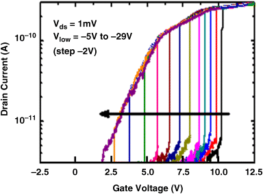
Figure 14.20 Measured I-V characteristics of an MOSFET with a movable gate electrode [18]. Very steep subthreshold characteristics are obtained
The drawback of the MOSFET with a movable gate is the leakage current from drain to source that is inevitable to the MOSFET structure. In order to completely shut down the leakage current, another type of MEMS switch has been also proposed and demonstrated [21,22]. Figure 14.21 shows schematics of a MEMS relay switch with zero standby power [22]. In this structure, the source and drain are suspended and its position is controlled by the gate. Since the source and drain are completely separated mechanically in the OFF state, no leakage current flows. At Vgs = 0 V, the source electrode is located above and the device is at the OFF state. At a certain voltage of Vgs, the “pull-in” takes place and the drain current suddenly increases with a very steep subthreshold slope. Figure 14.22 shows a circuit composed of MEMS relay switches [21]. An inverter operation as well as NAND and NOR operations have been successfully demonstrated.
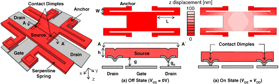
Figure 14.21 Schematics of a MEMS relay switch [20]. © 2009 IEEE (Left) Three-dimensional view of the device. (a) OFF state at Vgs = 0 V, where the source and drain are mechanically separated. (b) ON state, where the source and drain are physically contacted
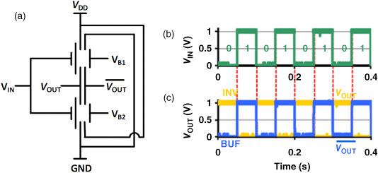
Figure 14.22 (a) A circuit schematic of a relay logic circuit. (b) Input signal. (c) Corresponding measured output signals [21]. © 2012 IEEE
14.4.6 Mott Transistor
It is well known that the abrupt resistance change by several orders of magnitude can be observed in the Mott metal–insulator transition. Mott field-effect transistor utilizes the electric field induced metal–insulator transition [23], in which the channel material shows both a metallic state and an insulating state controlled by the gate electrode. The Mott transistor could have a structure similar to conventional MOSFETs: the channel is composed of a correlated electron material, instead of semiconductor. Figure 14.23 shows schematics of the Mott metal-insulator transition and Mott transistor structure, where the channel material is VO2 [24]. The insulating/metallic states of the channel are controlled by the gate electric field. The sharp channel resistance change by the gate voltage has been successfully demonstrated. Figure 14.24 shows measured data of a Mott transistor composed of VO2 [24]. At low temperature, a large channel resistance change by a small change of gate voltage is observed.

Figure 14.23 Mott metal–insulator transition and Mott transistor using VO2 [24]. (a) The insulating state and metallic state. (b) Measured abrupt resistance change in strained 10 and relaxed 70 nm VO2 films. (c) A schematic of Mott transistor showing localized (insulating) electrons and delocalized (metallic) electrons. Reprinted by permission from Macmillan Publishers Ltd: [Nature] [26], copyright (2012)
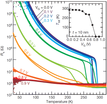
Figure 14.24 Experimental characteristics of a Mott transistor using VO2 [24]. A large change of channel resistance by only small change of gate voltage (VG) is observed. Reprinted by permission from Macmillan Publishers Ltd: [Nature] [26], copyright (2012)
Research on the Mott transistors is at a very early stage. The main challenges of the Mott transistors include a basic understanding of fundamental switching mechanisms, channel material selection, operating temperature, and stable transistor operation without hysteresis.
14.4.7 Bilayer Pseudo-spin Field-effect Transistor
In order to achieve ultimately energy-efficient information processing, a steep transition between the on state and off state in the 10 mV regime is necessary. BiSFET, bilayer pseudo-spin field-effect transistor, was recently proposed to enable the on/off transition at ultra-low voltage [25]. Figure 14.25a shows a schematic of the BiSFET structure that consists of an n-type and p-type graphene layer pair in close proximity, separated by a thin dielectric tunnel barrier. Both n-type and p-type grapheme layers have large and nearly equal carrier densities. Here, both electrons and holes are Fermions. However, under certain conditions, electrons in the n-type layer can pair with holes in the p-type layer, resulting in electron hole pairs/excitons which then condense even at room temperature in the case of the grapheme bilayer. Then, these are Bosons. This Bose–Einstein condensation alters the quantum wavefunctions in the bilayer qualitatively, resulting in a drastic reduction of the tunnel resistance between two layers for only a small interlayer bias. With a large bias, the condensation is destroyed leading to large resistance.
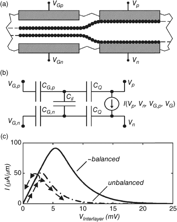
Figure 14.25 Structure, model, and I-V characteristics of BiSFET [25]. © 2009 IEEE (a) Schematic of a BiSFET. (b) Model circuit. (c) Modeled I-V characteristics
The device is called BiSFET because electron occupation of the top layer or bottom layer can be treated much like spin up or down, that is as a pseudospin, and the collective effects considered here are analogous to collective spin effects in a ferromagnet.
Figure 14.25b shows the circuit model and Figure 14.25c shows modeled current as a function of voltage between two grapheme layers of BiSFET [25]. A current peak appears in the I-V characteristics and then the current decreases at higher drain bias. Since the current change takes place at very low voltage (∼10 mV), very low voltage and low power operation may be possible. The simulations have shown that the energy consumption per clock cycle per BiSFET is 0.008 aJ at 100 GHz [25], while according to ITRS prediction MOSFET will consume 5 aJ per switching at 100 GHz in 2020 [1].
However, BiSFET is only a novel device concept. The main challenges include the fabrication of a perfect grapheme bilayer, a perfect gate stack with double gate structure, and an improved theory of the condensation.
14.5 Summary
In this chapter, recently proposed and/or reinvented transistors are reviewed. By closely looking at the historical trend of conventional MOSFETs in the past and comparing with the ITRS prediction, it is pointed out that one of the most significant challenge for future integrated electron devices is to attain high on-current with keeping low off-current at very low voltage, that is, a steep subthreshold slope. Newly proposed and reinvented transistors described in this chapter have great potential to solve this grand challenge.
References
- 1. International Roadmap Committee (2013) International Technology Roadmap of Semiconductors (ITRS) (http://public.itrs.net/).
- 2. Thompson, S., Anand, N., Armstrong, M. et al. (2002) A 90nm logic technology featuring 50nm strained silicon channel transistors, 7 layers of Cu interconnects, low k ILD, and 1 um2 SRAM cell. IEDM Tech Dig., pp. 61–64.
- 3. Mistry, K., Allen, C., Auth, C. et al. (2007) A 45nm Logic Technology with High-k+Metal Gate Transistors, Strained Silicon, 9 Cu Interconnect Layers, 193nm Dry Patterning, and 100% Pb-free Packaging. IEDM Tech. Dig., pp. 247–250.
- 4. Yokoyama, M., Kim, S.H., Zhang, R. et al. (2011) CMOS Integration of InGaAs nMOSFETs and Ge pMOSFETs with Self-Align Ni-Based Metal S/D Using Direct Wafer Bonding. Symposium of VLSI Technology, pp. 60–61.
- 5. Bangsaruntip, S., Joseph, E., Klaus, D. et al. (2010) Gate-all-around Silicon Nanowire 25-Stage CMOS Ring Oscillators with Diameter Down to 3nm. Symposium of VLSI Technology, pp. 21–22.
- 6. Auth, C., Allen, C., Blattner, A. et al. (2012) A 22nm High Performance and Low-Power CMOS Technology Featuring Fully-Depleted Tri-Gate Transistors, Self-Aligned Contacts and High Density MIM Capacitors. Symposium of VLSI Technology, pp. 131–132.
- 7. Takeuchi, K., Fukai, T., Tsunomura, T. et al. (2007) Understanding Random Threshold Voltage Fluctuation by Comparing Multiple Fabs and Technologies. IEDM Tech. Dig., pp. 467–470.
- 8. Tsunomura, T., Nishida, A., and Hiramoto, T. (2009) Verification of threshold voltage variation properties in scaled transistors with ultra large-scale device matrix array test element group. Japanese Journal of Applied Physics, 48 (12), 124505.
- 9. Mizutani, T., Yamamoto, Y., Makiyama, H. et al. (2012) Reduced Drain Current Variability in Fully Depleted Silicon-on-Thin-BOX (SOTB) MOSFETs. IEEE Silicon Nanoelectronics Workshop, pp. 71–72.
- 10. Fuketa, H., Yasufuku, T., Iida, S. et al. (2011) Device-Circuit Interactions in Extremely Low Voltage CMOS Designs. IEDM Tech. Dig., pp. 559–562.
- 11. Jung, S.-M., Saraya, T., and Hiramoto, T. (2013) Effect of Drain Voltage Dependent Subthreshold Voltage Reduction on Energy Efficiency in Steep Subthreshold Slope Transistors. Japan Applied Physics Society Spring Meeting, 29a G9-3.
- 12. Gopalakrishnan, K., Griffin, P.B., and Plummer, J.D. (2002) I-MOS: A Novel Semiconductor Device with a Subthreshold Slope lower than kT/q. IEDM Tech. Dig., pp. 289–292.
- 13. Seabaugh, Alan C. and Zhang, Qin (2010) Low-voltage tunnel transistors for beyond CMOS logic. Proceedings of the IEEE, 98 (12), 2095–2110.
- 14. Ionescu, A.M. and Riel, H. (2002) Tunnel field-effect transistors as energy-efficient electronic switches. Nature, 479, 329–337.
- 15. Huang, Q., Huang, R., Zhan, Z. et al. (2012) A Novel Si Tunnel FET with 36mV/dec Subthreshold Slope Based on Junction Depleted-Modulation through Striped Gate Configuration. IEDM Tech. Dig., pp. 187–190.
- 16. Dewey, G., Chu-Kung, B., Kotlyar, R. et al. (2012) III-V Field Effect Transistors for Future Ultra-Low Power Applications. VLSI Tech. Symp., pp. 45–46.
- 17. Tomioka, K., Yoshimura, M., and Fukui, T. (2012) Steep-slope Tunnel Field-Effect Transistors using III-V Nanowire/Si Heterojunction. VLSI Tech. Symp., pp. 47–48.
- 18. Salvatore, G.A., Bouvet, D., and Ionescu, A.M. (2008) Demonstration of Subthrehold Swing Smaller Than 60mV/decade in Fe-FET with P(VDF-TrFE)/SiO2 Gate Stack. IEDM Tech. Dig., p. 167–170.
- 19. Rusu, A., Salvatore, G.A., Jiménez, D., and Ionescu, A.M. (2010) Metal-Ferroelectric-Metal-Oxide-Semiconductor Field Effect Transistor with Sub-60mV/Decade Subthreshold Swing and Internal Voltage Amplification. IEDM Tech. Dig., pp. 395–398.
- 20. Park, J.S., Saraya, T., Miyaji, K. et al. (2008) Characteristic Modulation of Silicon MOSFETs and Single Electron Transistors with a Movable Gate Electrode. IEEE Silicon Nanoelectronics Workshop, p. S1015.
- 21. Liu, T.-J.K., Hutin, L., Chen, I.-R. et al. (2012) Recent Progress and Challenges for Relay Logic Switch Technology. VLSI Tech. Symp., pp. 43–44.
- 22. Kam, H., Pott, V., Nathanael, R. et al. (2009) Design and Reliability of a Micro-Relay Technology for Zero-Standby-Power Digital Logic Applications. IEDM Tech. Dig., pp. 809–812.
- 23. Newns, D.M., Misewich, J.A., Tsuei, C.C. et al. (1998) Mott transition field effect transistor. Applied Physics Letters, 73, 780–782.
- 24. Nakano, M., Shibuya, K., Okuyama, D. et al. (2012) Collective bulk carrier delocalization driven by electrostatic surface charge accumulation. Nature, 487, 459–462.
- 25. Banerjee, S.K., Register, L.F., Tutuc, E. et al. (2009) Bilayer PseudoSpin field-effect transistor (BiSFET): a proposed new logic device. IEEE Electron Devices Letters, 30, 158–160.