
16
Carbon Nanotube Electronics
Aaron D. Franklin
Department of Electrical and Computer Engineering and Department of Chemistry, Duke University, USA
16.1 Carbon Nanotubes – The Ideal Transistor Channel
What made silicon so attractive for use as the transistor industry's foremost semiconducting material was primarily its accessibility compared to semiconductors with more ideal attributes. Compared to germanium, on which the early field-effect transistors (FETs) were demonstrated, silicon had a less desirable indirect bandgap and much lower mobility for electrons and holes. However, silicon was (and is) abundant and had a native oxide, SiO2, which proved viable as a gate dielectric and an excellent passivation layer for surface states. After over five decades of shrinking down the size of silicon metal-oxide-semiconductor FETs (MOSFETs), the scaling limit is now effectively reached and industry is clamoring for a more scalable and more ideal replacement. This chapter presents the single-walled carbon nanotube (CNT) as the ideal semiconducting material for yielding scalable, high-performance FETs for the next generation of electronics.
16.1.1 Electronic Structure of a CNT
Physically, a CNT is composed of a single cylindrical shell of carbon atoms that are sp2-bonded in a honeycomb lattice. It is instructive to consider the CNT as a sheet of graphene rolled into a seamless cylinder, providing both visual conception and insight into the electronic structure of a nanotube. Consider the carbon lattice for graphene in Figure 16.1, shown in both real and reciprocal space. The two unit vectors, a1 and a2 can define the location of all atoms in the lattice. A CNT is described by a chiral vector c = ma1 + na2, which indicates the folding of one atom in the lattice onto another to form the nanotube. The “rolling” of the lattice into a CNT with a diameter dCNT between 0.8 and 2.5 nm results in a quantization of the electronic states in the circumferential direction, as represented by the parallel lines in Figures 16.1b and 16.2. Each of the parallel lines is a subband with its own set of 1D dispersion relations. The subbands are determined by the periodic boundary condition around the circumference of the CNT, with a circumferential wave vector kc such that kc c = kc|c| = kcπdCNT = 2πν, which defines a series of parallel lines, each corresponding to a different integer value for ν.
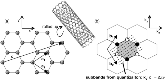
Figure 16.1 (a) Graphene's honeycomb lattice of carbon atoms in real space, with unit vectors a1 and a2, and an example chiral vector c illustrated as c = ma1 + na2 = 3a1 + a2. (b) Graphene's lattice in reciprocal space showing unit vectors b1 and b2 with the Brillouin zone shaded. Dashed lines represent the allowed states in ky that result from quantization in the circumferential direction from the “rolling” of a graphene sheet to form a CNT

Figure 16.2 (a) Illustration of a first Brillouin zone for graphene with the conical energy dispersions shown at each K point. The quantized k-states for a nanotube's 1D subbands are depicted as parallel dashed lines. (b, c) A closer look at the dispersion relation for a subband passing (b) through a K point to form a metallic CNT and (c) away from a K point to form a semiconducting CNT
As illustrated in Figure 16.2, if a subband passes through one of the corners (known as K points in reciprocal space) of the Brillouin zone then the CNT will have no energy bandgap (Eg) and thus exhibit metallic properties. However, if none of the subbands pass through the K points, then the CNT will be semiconducting with a direct bandgap between the conduction and valence band. The bandgap is proportional to the smallest distance between a K point and the subband lines. Upon accounting for the threefold symmetry of the K points, the bandgap for a CNT becomes:
where ![]() is Planck's constant and vF is the Fermi velocity of electrons.
is Planck's constant and vF is the Fermi velocity of electrons.
Entire chapters have been written on the electronic structure of CNTs [1–3], but most of the crucial aspects can be gleaned, or extrapolated, from the information presented thus far, including:
- Semiconducting CNTs have a direct bandgap that is inversely proportional to dCNT.
- “Rolling” of a 2D graphene lattice to form a CNT produces 1D subbands around the circumference of the nanotube.
- Effective mass of electrons and holes is equal (slope of conical dispersion relations is symmetric around the K points).
16.1.2 Electron Transport in CNTs
Because of quantum confinement in the circumferential direction, electron transport in CNTs is effectively 1D – carriers can either move forward or directly backward – with the carrier wave function traversing around the nanotube [3]. Carrier scattering is predominantly a result of acoustic and optical phonons. Acoustic phonon scattering is elastic and exhibits a long mean free path for CNTs on the order of 300 nm. The emission of optical phonons, however, is inelastic and has a much smaller mean free path of ∼10–15 nm, though high fields are required for these scattering events (> 0.16 eV) [4–7].
An important question for a 1D material is what the minimum resistance would be if the injection of carriers at the contacts is perfect and there is no carrier scattering? The current in such a device would simply be the product of excess carrier density (Δn), carrier velocity (v) and the elementary charge of an electron (e):
where the application of a voltage between the drain and source contacts is Vds, which opens a certain number of states in the 1D channel for transport based on the density of states, D. D and v are obtained from the parabolic dispersion relation, with dependence on Planck's constant (h) and the carrier effective mass (m). The result in Equation 16.2 is for most 1D materials with perfect transmission and no scattering; but for a CNT, the twofold band degeneracy of the K points at the Fermi level yields an extra factor of two in the current and thus the following minimum resistance/conductance:
This quantum of resistance is the lowest possible resistance per subband for an electrically contacted CNT in the absence of scattering. Note that RQ is for both of the needed contacts, source and drain, so there is effectively 3.25 kΩ per contact. There have been several experimental demonstrations of reaching the ballistic transport limit in CNTs [7–12], two of which are shown in Figure 16.3. It is unlikely that there will ever be perfect transmission of carriers at the contacts, especially for semiconducting CNTs where Schottky barriers are typically present [13–16], and thus the best realizable resistance per nanotube in a transistor is between 6.5 and 12 kΩ.
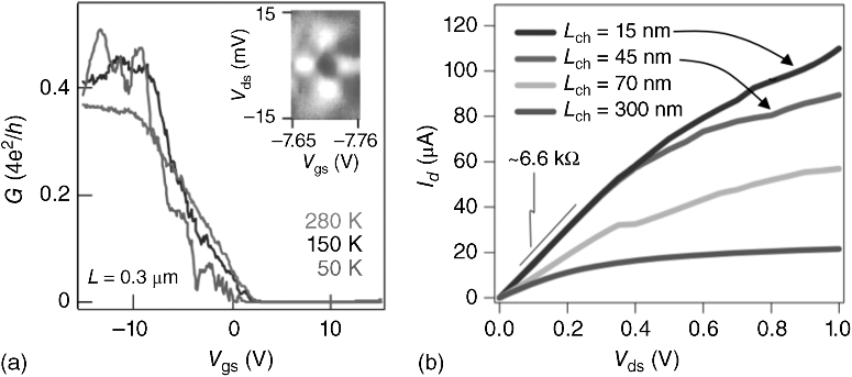
Figure 16.3 Demonstrations of reaching ballistic transport in CNTs. (a) CNT transistor with G = 0.5GQ at a 300 nm channel length [8]. (b) Metallic CNT devices down to 15 nm in length showing that below ∼50 nm the device resistance at low fields is at the ballistic limit, Rtot ∼ RQ [7]. Reprinted by permission from Macmillan Publishers Ltd: Nature [8], copyright 2003 and Nature Nanotechnology [7], copyright 2010
16.1.3 The Ideal Transistor
As this book shows, there are a variety of options for a new digital switch that can replace silicon MOSFETs with higher performance, lower power, and more scalability. Aside from the dramatic platform-changing devices, such as spintronics and NEMS, most engineers can agree on what the ideal attributes would be for the channel material in a field-effect transistor. First, the ideal material should have ballistic transport for electrons and holes, be ultra-thin to maximize scalability, and have a bandgap of at least 0.5 eV. The gate should be able to wrap completely around the channel for optimal electrostatics and to eliminate the influence of stray charges or screening interactions. Finally, the semiconductor should be able to operate at low voltages while delivering high current density.
Juxtaposing CNTs against this profile of the ideal FET channel shows why they have received, and continue to receive, so much attention as an excellent candidate for silicon replacement. Their 1D nature exhibits ballistic transport, they are a mere ∼1 nm in diameter/thickness, lend themselves perfectly to a gate all around geometry, and have been shown to provide high performance at low voltages. While there are certainly many material and engineering challenges that remain for CNTFETs, the impressive progress that has been made in the field combined with the CNT's ideal attributes for FETs suggest they are worth further pursuit. The proceeding sections will review the latest progress in the field and provide a brief overview of the challenges that remain.
16.2 Operation of the CNTFET
The first demonstrations of modulating a CNT channel using a gate-induced field came in 1998 [17,18]. These early CNTFETs, along with the majority of those studied since, were fabricated by using a doped silicon substrate gate to modulate the energy bands of a metal-contacted CNT, which was separated from the gate by a thermal SiO2 gate oxide as depicted in Figure 16.4a. Since then, a variety of CNTFET structures have been demonstrated and can primarily be classified into devices with and without spacers. For a CNTFET, the spacer length (Lspr) is the distance between the gated channel and the source/drain metal contacts, as shown in Figure 16.4b and c.
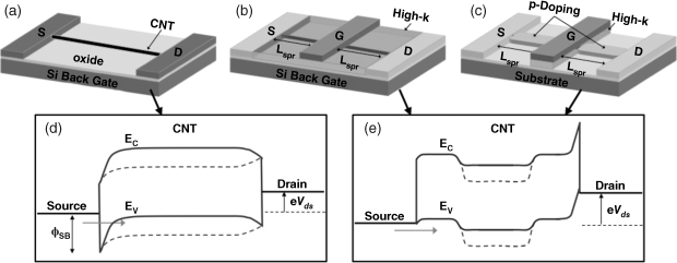
Figure 16.4 Example schematics and band diagrams of prominent CNTFET structures. Schematics of (a) substrate-gated, (b) gated-spacer, and (c) doped-spacer CNTFETs. Energy band diagrams illustrating the on state (solid lines) and off state (dashed lines) of a CNTFET (d) without spacers and (e) with gated/doped spacers
For CNTFETs without spacers, a band diagram illustrating the basic operation is given in Figure 16.4d. Regardless of whether the gate is on bottom or top of the CNT channel, the operation of these spacer-less devices is nominally the same. Because nanotubes are intrinsic semiconductors, carriers are not induced in the channel by the gate-field, but must be injected from the contacts by the gate lowering the thermal barrier in the channel and the carriers tunneling through the Schottky barrier (SB) at the source (if there is a SB). Therefore, the contact metal work function plays a significant role in CNTFET performance, as will be discussed in Section 16.3.1. Note that the applied Vds is dropped entirely at the drain-end of the device based on the ballistic transport nature of the CNT channel. Several studies have explored the impact of dropping the bias across such a small (few nanometers) length and the resultant heating of the contacts [6,19,20], which only limits the performance at very high fields where breakdown of the CNT can occur locally.
In contrast to the spacer-less devices, CNTFETs with spacers are less limited by injection at the metal-CNT source – owing to the high level of doping in the spacers from either a molecular dopant or “electrostatic doping” from a gate that thins the SB – and are controlled primarily by the gate modulating the thermal barrier in the channel, like conventional MOSFETs [21]. Note that a CNTFET with spacers that are not doped in some fashion will have a large series resistance across Lspr, blocking carrier transport between the channel and source/drain – spacers in CNTFETs are therefore much like source/drain extensions in MOSFETs. CNTFETs with spacers will also be more resistant to ambipolar conduction because of the larger barrier to carrier injection at the drain [22,23]. Ambipolar conduction – conducting electron and hole currents in a device depending on the gate voltage – in CNTFETs has been seen as a great concern because a device would not remain in the off state if the gate bias is swept too far. Hence, a CNTFET that can suppress such ambipolarity is very attractive. Regardless of the CNTFET structure, movement of the energy bands by the gate in the on state can nominally be maintained at 1: 1 by operating the device in the quantum capacitance limit – uniquely accessible because of the 1D CNT [24–26].
16.3 Important Aspects of CNTFETs
As was introduced in the preceding section, there are a few key aspects to a CNTFET that impact the operation and performance, including the contacts, dielectrics, gate structure, and passivation treatments. Over the years, the research community has improved each of these important components, with far too much progress to cover in this short section. Therefore, emphasis herein is given to a brief summary of each aspect and the latest status in the field.
16.3.1 Contacts
Because CNTs are intrinsic semiconductors, all carriers must enter the channel by injection from the contacts, making the metal source/drain to CNT interface extremely important in CNTFET performance. For semiconductors that have dangling bonds at their surface, Fermi level pinning severely limits the effect of using metal contacts with different work functions to tune carrier injection [27]. However, CNTs have no open bonds on their honeycomb carbon lattice and hence are not impacted by such pinning of the metal Fermi level to certain mid-bandgap states [28]. Without Fermi level pinning, the choice of metals with appropriate work functions is a valuable method for maximizing performance and even tuning polarity in CNTFETs.
Many metals have been explored as source/drain contacts to CNTs [8,9,23,29–32]. Perhaps most significant was the discovery that Pd creates a nearly ideal p-channel contact to the valence band of CNTs [8]. Several studies on how metal work function and CNT diameter both contribute to a certain SB height have been reported, including the exploration of Pd, Ti, and Al contacts shown in Figure 16.5 [33]. While this data suggests a clear relationship between the metal work function and resulting SB height, there are other aspects to consider. For instance, Pt, which has a work function of 5.65 eV, provides a very poor contact to CNTs despite its work function being larger than Pd [8]. The reason for this inconsistency is that the physical wetting of a metal on a CNT, also referred to as coupling, is another critical factor for carrier injection [24,34,35].
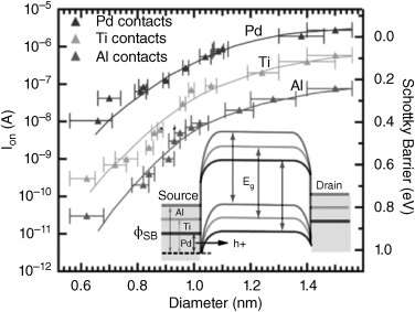
Figure 16.5 On current (Ion) and Schottky barrier height dependence on CNT diameter, which is inversely proportional to the bandgap, for contact metals with different work functions. Inset is a band diagram illustrating how the contact metal affects the SB height (ϕSB) for a CNT with the same bandgap for each metal. Adapted with permission from [33]. Copyright 2005 American Chemical Society
A final consideration for the contacts is regarding their geometric coverage of the CNT. Most devices have used contacts that are on top of the nanotube, interfacing noncovalently with the sp2-bonded carbon. Yet, some theoretical studies have suggested that metal contacts to the “ends” of a nanotube, where the carbon bonds are dangling, can provide many times lower contact resistance [36]. Experimental data has yet to defend or deny this claim, though Pd top contacts have already yielded CNTFETs with resistances very near RQ [7,9], suggesting that there is not much that can be improved by employing different contact geometries for Pd so long as the contact length is greater than the transfer length (see Section 16.4.2).
16.3.2 n-Type CNTFETs
With a work function of ∼4.7 eV [37,38], the Fermi level at mid-gap, no metal-induced gap states causing Fermi level pinning, and an average bandgap of 0.6 eV, CNTs naturally lend themselves to p-type FETs because of the easiness of finding a robust high work function metal for injecting holes into the valence band (see Figure 16.5). Based on the common CNTFET structures in Figure 16.4, obtaining an n-type CNTFET – where electron injection is favored – can be achieved by either doping the spacer regions and/or using a low work function metal.
Doping CNTs is difficult to control. As mentioned previously, substitutional or interstitial doping is not available, so the dominant method is to apply a layer of charged molecules to the CNT surface. This has been done in gas [39,40] or solution [41,42] phase, and with both n- and p-type dopants. While this charge-transfer doping approach has enabled some high-performance CNTFETs, it is not without challenges, including: (1) low consistency/uniformity, (2) instability in air, (3) low compatibility with subsequent planarization of devices, and (4) sensitivity to high temperatures. Every molecular dopant does not necessarily have all of these challenges, but they each have at least one of them to some degree. An example of a high performance n-type CNTFET achieved by applying a layer of charged molecules to the spacer, or source/drain extension, regions of a Pd-contacted device is given in Figure 16.6a [40]. Note that a further advantage of having a CNTFET device with doped spacers is that the undesirable ambipolar conduction is largely subdued because of the sizeable barriers to carrier injection at the drain.
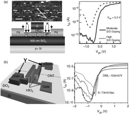
Figure 16.6 Schematic and corresponding subthreshold curves from n-type CNTFETs achieved by (a) doping the spacer (source/drain extension) regions with charged molecules [40] and (b) using low work function Y metal contacts for small SB to the conduction band [43]. Adapted with permission from [40] and [43]. Copyright 2005 [40] and 2009 [43] American Chemical Society
Establishing metal contacts with low barriers to electron injection is critical for n-type CNTFETs, even those with doped spacers (though in the case of doped spacers the SBs are thinned substantially by band movement from the doping). Perhaps the greatest challenge in working with low work function metals is their high propensity to oxidize, which among other things compromises their air stability and consistency of material quality. However, with appropriate passivation layers used to cap the metals, there have been demonstrations of n-type CNTFETs having superb performance, primarily using Y [43], Sc [11], or Er [44]. The subthreshold curves from the device in Figure 16.6b with Y contacts exhibit near ideal performance for a single CNT – as good as p-type devices from Pd contacts. It has even been shown that, under the appropriate metal deposition conditions, the yield of n-type CNTFETs can be increased to the level achievable by high work function metal p-type devices [44]. While more difficult to achieve than p-type CNTFETs, high performance n-type devices have become accessible and no longer prove to be a bottleneck to a CNT technology.
16.3.3 Dielectrics
As pointed out previously, CNTs are made up of fully satisfied covalent carbon bonds. For this reason, choosing a dielectric for CNTFETs is not related to Fermi level pinning or passivating surface states – as is the case for most other semiconductors and the plague for III-V materials [45] – but rather what dielectric can be scalable with a compatible deposition process for the CNT. The most common fabrication method for depositing high quality high-κ dielectrics is atomic layer deposition (ALD), which is a chemical vapor deposition process that relies on gaseous precursors to react with surface states to form a dielectric one layer at a time [46]. Having no surface states, CNTs are not naturally compatible with ALD. To overcome this limitation, bottom-gate CNTFETs have been used [47,48] or adhesion layers have been applied to enable ALD nucleation on CNTs [49,50]. These adhesion layers can cause undesirable perturbations to carrier transport in the CNT without the appropriate annealing treatments applied during processing [51].
For bottom-gated devices the dielectric is completely formed prior to placing the nanotubes on the substrate, making it a great option as far as dielectric choice, scalability, and quality are concerned. But, the bottom gate geometry can also be tricky for manufacturability (see Section 16.3.5), so it is desirable to have other options. Adhesion layers for ALD nucleation have been demonstrated in the form of DNA molecules that wrap CNTs [52] or gas-phase functional layers formed in a CVD chamber prior to ALD [49]. The latter approach is more favorable in that it employs compatible oxide layers that will not compromise the needed low equivalent oxide thickness (EOT) of the final device structure. Once the adhesion layer is in place, ALD can be used to deposit the high-κ material of choice.
16.3.4 Passivation Treatments
One highly promoted application space for CNTFETs is in chemical or biological sensing [53–55]. Because of their small size and extremely high specific surface area, the presence of virtually any adsorbate is readily detected by conductance changes in a CNT. While excellent for sensing applications, the nanotube sensitivity to such stray charges is a challenge for high performance digital applications. This difficulty is manifest in the large variation of threshold voltage (Vt) among CNTFETs of the same geometry and the sizable hysteresis that is standard for most CNTFETs [56].
Transfer curves from a set of CNTFETs built on the same nanotube are shown in Figure 16.7, where the threshold voltages span a range of ∼0.8 V. The simple application of a hydrophobic self-assembled monolayer in vacuum to passivate (cover) the exposed CNT channel and surrounding dielectric surface is able to reduce the range of Vt by more than 50%. This reduction in Vt variation is a result of the vacuum deposition environment driving off stray charge adsorbates (e.g., oxygen, water) and then passivating the hydroxylated surface to stave off any future adsorbates. Further, the hysteresis in the same devices was reduced on average from 500 mV to <50 mV over a gate source bias (Vgs) range of 4 V at Vds = −0.5 V. Such a dramatic reduction in variability is evidence that the variation is not intrinsic to the CNTs and is primarily a result of the channel being susceptible to stray charges in the vicinity. Hence, either a technologically compatible passivation coating that can eliminate such charge, or the ability to completely wrap a CNT in the gate is needed to address the variability problem.
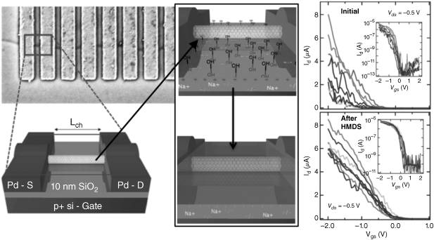
Figure 16.7 CNTFETs constructed along the same CNT showing large variation in threshold voltage. Gas-phase application of a hydrophobic monolayer passivates the hydroxylated surface and substantially lowers variation among the devices. Adapted with permission from [56]. Copyright 2012 American Chemical Society
16.3.5 Gate Structure
Because CNTs are not substrate-bound, there is a lot of freedom in designing the gate structure. As shown in Figure 16.4, CNTFETs are typically fashioned with either bottom- or top-gate geometries. While the top-gate does provide an omega-shaped gate structure, the electrostatics are not appreciably different from the bottom gate, cylinder on plate, structure. Top gates more closely mimic the structure of Si MOSFETs, but have been challenging to realize with the difficulty of nucleating dielectrics on CNTs (see Section 16.3.3) and the inability to use reactive ion etching (RIE) in the presence of CNTs (nanotubes are readily etched away in a reactive ion environment).
For local bottom gate devices, there is no fabrication limit to the scalability of the dielectric thickness (tox) because it is formed prior to CNT placement, thereby minimizing the number of processing steps that the nanotubes are exposed to and preserving their quality. Another advantage of bottom gates is that they allow for any choice of passivation/planarization/capping layer to be used to cover the final device (see Section 16.3.4), rather than being restricted to the gate dielectric layer as in top-gate structures. Regardless of the gate geometry, the gate metal work function provides a 1 : 1 control over the device threshold voltage to enable the tuning of Vt in a final architecture [57].
The ultimate gate structure for CNTFETs is one that completely wraps the nanotube channel in a gate-all-around (GAA) fashion [50,58]. GAA is so natural for CNTs that it has been used for virtually all simulation studies of CNTFETs [59–61]. A demonstration of GAA-CNTFETs is given in Figure 16.8 [51]. Although the GAA provides the ideal electrostatic structure for nanotubes, it is a mistake to conclude that this marginal improvement in electrostatics is critical for achieving CNTFETs with sub-10 nm channels (see Section 16.4.1). The ultrathinness of a nanotube (<2 nm) enables excellent gate control of the channel even with only a bottom gate [62]. Actually, the primary motivation for GAA is that the gate encompasses the CNT, shielding it from stray charge, screening interactions, or other local variations. As pointed out in Section 16.3.4, nanotubes are sensitive to any charge in their vicinity, and the GAA is the only complete solution for addressing this challenge.
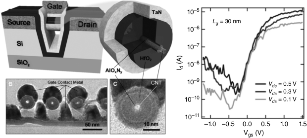
Figure 16.8 CNTFET with a gate-all-around (GAA) geometry. The transmission electron microscope images are cross-sections of the GAA-CNT showing uniform coating of the gate stack on the nanotube(s). Subthreshold curves are from a 30 nm gate length n-type GAA-CNTFET. Adapted with permission from [51]. Copyright 2013 American Chemical Society
16.4 Scaling CNTFETs to the Sub-10 Nanometer Regime
In order for a transition from mainstream Si MOSFET technology to be worthwhile, the replacement must provide substantial benefits in performance at sub-10 nm dimensions – a regime where silicon of any dimensionality cannot compete. Therefore, while CNTFETs were shown for years to have excellent performance at hundreds of nanometers, verification of their scaled performance benefits is crucial. The two critical lengths for scaling in a CNTFET are the channel length (Lch) and contact length (Lc) as illustrated in Figure 16.9.
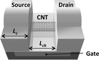
Figure 16.9 Schematic of a CNTFET with the contact and channel lengths identified
16.4.1 Channel Length Scaling
Scaling down the channel length of a CNTFET has enabled ballistic transport and high on currents [7,9,63,64]. The danger with aggressive Lch scaling in any FET is that the gate will lose control over the energy bands in the channel – a problem known as short channel effects (SCEs). Because of their ultrathin body, CNTs have been projected to provide excellent gate control at scaled lengths. However, with very small carrier effective mass, CNTs are also susceptible to source–drain tunneling, which is another SCE that causes an increase in subthreshold swing (SS) and off current. Some theoretical projections suggested that such tunneling would be the demise of CNTFETs at Lch <15 nm [59,60].
Over the years, experimental CNTFETs with channels between 15 and 300 nm were demonstrated with little to no SCEs. It was not until 2012 that Lch was scaled below 10 nm for a CNTFET [62], and the result defied previous theoretical expectations. The 9 nm CNTFET did not exhibit the anticipated SCEs, such as high SS, and instead performed better than any silicon-based device of comparable length, as shown in Figure 16.10. Importantly, the comparison of on currents in Figure 16.10 has been pitch-normalized, which accounts for the fact that you can only pack CNTs or fins or nanowires so close to each other and still be able to fit all of the gate stack. In the case of CNTs, the device was a local bottom gate, where there would be no gate stack to limit the pitch, though a reasonable 5 nm pitch was chosen.
Figure 16.10 (a) Subthreshold curves from a CNTFET with a 9 nm channel length. (b) Subthreshold swing versus channel length for CNTs compared to the best experimentally demonstrated silicon-based FETs. On current (Ion) is pitch-normalized for CNTs (5 nm pitch) and fins/nanowires (20 nm pitch) and extracted at |Vgs − Vt| = 0.3 V and |Vds| = 0.5 V (the needed voltages for a VDD = 0.5 V technology). Adapted with permission from [62]. Copyright 2012 American Chemical Society
16.4.2 Contact Length Scaling
It is instinctual to focus on channel length when discussing the scaling of any type of FET because SCEs are known to be a result of small Lch. However, for an FET to be densely integrated in a useful digital technology, the length of the contacts (source and drain) must be scaled as aggressively as the channel. The fact that there has been less focus on Lc scaling for nanoelectronic devices is not because it has not been a challenge for Si MOSFETs – small contact lengths have led to dramatic increases in series resistance, which compromises on state performance. It is most probable that the lack of attention to Lc in nanomaterial-driven FETs is simply because: (1) SCEs from Lch scaling is a bigger concern for Si MOSFETs and thus more popular to address and (2) there is less motivation to consider Lc when there are still SCEs present.
For CNTFETs, the first study to consider the impact of contact scaling revealed an important challenge for realizing high performance, ultrasmall devices: contact resistance (Rc) exhibits an inverse dependence on Lc, similar to MOSFETs [7,35]. While some previous studies had explored this trend for large multi-walled carbon nanotubes [65], this Rc versus Lc dependence in CNTFETs, shown in Figure 16.11, clearly defined the balance between Lch and Lc scaling in these devices for achieving optimal performance.
Figure 16.11 (a) Schematic and corresponding scanning electron microscope image of a set of CNTFETs with different contact lengths assembled along the same long CNT. (b) Contact resistance versus contact length from three sets of CNTFETs, each assembled on a different CNT. Adapted with permission from Macmillan Publishers Ltd: Nature Nanotechnology [7], copyright 2010
The reason for Rc showing strong dependence on Lc is different than for MOSFETs. A metal-CNT contact is a 3D-1D, metal–semiconductor interface, creating a very different scenario from the standard 3D-3D, silicide–semiconductor interface. Some had even projected short contacts to improve metal-CNT Rc by maximizing the electric field at the interface [13,66]. There have been theoretical studies that try and make sense of the observed scaling behavior, but they all deal with carrier injection between the metal-CNT and have not found a way of considering how transport in the metal-covered CNT contributes to Rc [34,35,67,68]. Overall, this result is still rather new and has only been shown for one contact metal, Pd. There are a myriad of possibilities for improving the Lc scaling behavior for CNTFETs that should come to light in the ensuing years.
16.5 Material Considerations
The focus of this chapter has predominantly been on the device considerations for a high-performance CNTFET technology. However, as with any relatively new material, CNTs have unique challenges at the materials-level that must be addressed in order for them to be viable for a densely integrated technology. The two prominent challenges are the isolation of semiconducting CNTs and the positioning of these CNTs on a substrate.
16.5.1 High-Purity Semiconducting CNTs
As discussed in Section 16.1.1, depending on the chirality of a nanotube it can either be metallic or semiconducting. The tolerance for a metallic nanotube in technologically relevant CNTFETs is very low at ∼0.0001%. Statistically, the distribution of metallic versus semiconducting nanotubes is 1: 2, meaning 33% are metallic. Over the years, progress has been made in separating semiconducting CNTs from their metallic counterparts, as shown in Figure 16.12. The most promising techniques involve dispersion of CNTs into solution and then using some type of chemical technique for differentiating the semiconducting from the metallic, such as density gradient ultracentrifugation [69–71], column chromatography [72], or DNA coating [73]. Many reviews have been written comparing the various techniques that have been demonstrated [71,74]. The target purity is 99.9999% semiconducting [75], with the best reported as of early 2013 being 99.9% [76]. While the remaining three orders of magnitude in needed purity is daunting, it is not fundamentally impossible [77], albeit difficult to characterize.
Figure 16.12 Progress in isolating semiconducting CNTs over the years, including both solution phase (CNTs dispersed in a solution) and substrate-supported (CNTs on substrate) techniques. The target for a technology is ∼99.9999%
16.5.2 Precise Placement of CNTs
One of the core differences between CNTFET fabrication processes and those of MOSFETs is that they are bottom-up versus top-down approaches, respectively. A MOSFET is created out of a bulk material – doped, annealed, patterned, coated, and so on. A CNTFET is assembled by synthesizing and placing (sometimes in one step) CNTs in desired locations and then establishing contacts, dielectrics, and gates onto them. This bottom-up approach has some advantages, including substrate independence and many contact/gate material options. The primary disadvantage is the difficulty of precisely positioning CNTs at a certain pitch (see Figure 16.13) across an entire wafer.
Figure 16.13 Progress in placing CNTs on a substrate at a certain linear density (number of CNTs per micron). Placing CNTs at an inconsistent pitch has reached a higher density but suffers from a lack of uniformity. The target is for at least 125 CNTs/μm (pitch ≤ 8 nm)
There has been considerable progress in the precise placement of CNTs [77], as shown in Figure 16.13. The highest reported linear density is ∼55 CNTs/μm [78], though the pitch of the CNTs was inconsistent. Inconsistent pitch leads to challenges for fabricating CNTFETs with a controllable number of CNTs in each channel. Furthermore, if nanotubes are too closely spaced without being electrically isolated from each other, then charge-screening interactions will also be present and nonhomogeneous [79–82]. Placement of CNTs with uniform pitch has not progressed as rapidly, but is improving as techniques involving nanotube and/or substrate functionalization continue to advance [83–87]. The best linear density at a controlled pitch is 10 CNTs/μm [87], which is approximately an order of magnitude away from the target of at least 125 CNTs/μm [75].
16.6 Perspective
This chapter has shown that CNTFETs are aggressively scalable and have been experimentally demonstrated to outperform competing devices at low voltages. As with all “next switch” logic devices, there are challenges that remain to realizing a CNTFET technology, most of which have been reviewed in Sections 16.4 and 16.5. Should these obstacles be overcome, where would CNTFETs be expected to show up on the transistor roadmap? First it must be decided which of the roadmaps CNTFETs are best suited for. The most obvious is that of high performance digital computing, which CNTFETs have been anticipated to compete in for most of their lifetime. A technologically relevant CNTFET in this space is projected to have 5–6 CNT channels in each device, as shown in Figure 16.14a. To get an idea of how a CNTFET technology would perform compared to other options for the sub-10 nm technology nodes, a power–performance simulator was built that optimizes each device's dimensions for the best power–performance trade-off. As shown in Figure 16.14b, CNTFETs are projected to enable a technology with ∼3× greater efficiency along with ∼3× higher performance than FinFETs for a constant chip power density [75]. This level of power–performance improvement is very motivating for pursuit of a CNTFET technology in the high performance digital space.
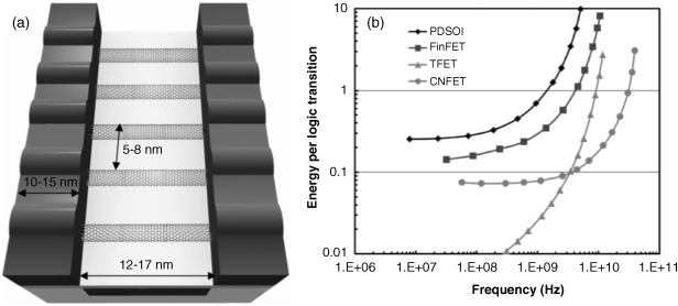
Figure 16.14 (a) Schematic of technologically relevant CNTFET device for 5 nm technology node, including 5–6 CNTs at a pitch of 5–8 nm. The noted channel length includes any spacer (source/drain extension) lengths. (b) Power versus performance simulation mimicking a P7 microprocessor architecture (1.5 M logic gates, four cores) comparing CNTFET (CNFET) to tunnel FETs (TFET), silicon FinFETs, and partially depleted silicon on insulator FETs (PDSOI) at the 7 nm technology node, with CNTFETs yielding a 3× better efficiency and 3× higher performance than FinFETs at a fixed chip power density [75]
Another way to view the type of performance that CNTFETs can offer compared to the competition is to consider relevant projected and demonstrated parameters, as shown in Table 16.1. Throughout this book, nanoelectronic devices that compete for the same application space as CNTFETs have their parameters listed in a similar fashion, providing a clear picture of the advantages available from each device and how close the promised parameters are to being demonstrated. As seen in Table 16.1, CNTFETs have very nearly demonstrated the projected performance for all of the important metrics.
Table 16.1 Summary parameter table of CNTFETs
| Parameter | Values for the device in this chapter | |
| Gate length Lg | Demonstrated | 9 nm |
| Projected | 5 nm | |
| Subthreshold Swing SS | Demonstrated | 60 mV/dec |
| Projected | 60 mV/dec | |
| Device speed, gate delay τ | Demonstrated | 2 ps |
| Projected | 0.42 ps | |
| Operation voltage VDD | Demonstrated | 0.4 V |
| Projected | 0.25 V | |
| On current at VDD = 0.5 V (normalized over contact width not CNT diameter) | Demonstrated | 0.6 mA/μm |
| Projected | 2 mA/μm |
While ideally suited for application in the high performance digital space, CNTFETs are also very promising for radio frequency (RF) electronics [88–92]. With the ability to carry high currents, a reportedly high linearity, and a bandgap that allows for current saturation, many see nanotubes as more suited for RF than graphene, which has received much more attention in the RF device community. The same materials challenges that face CNTFETs for digital are hedging the way for RF applications, though the needed deliverables in purity and placement density are more relaxed for RF [93].
The other roadmaps that a CNTFET technology could very well contribute to, if not completely enable, are those of flexible and/or transparent electronics. While there are a few other nanoelectronic devices that could be applicable to these fields, the CNTFET is one of the best performing and potentially the most accessible. There have already been a number of demonstrations of flexible and/or transparent circuits built using CNTFETs [94–99], as shown in Figure 16.15. These devices tend to be thin-film transistors (TFTs), which have less stringent performance, scaling, and fabrication requirements as they are traditionally assembled using large films of CNTs to make devices with large feature sizes. Ultimately, even the best performing CNTFETs would be compatible with these exotic substrates owing to their bottom-up fabrication.
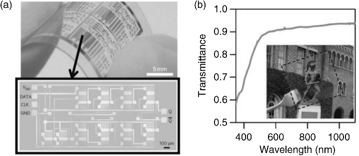
Figure 16.15 Examples of (a) flexible [94] and (b) transparent [95] CNTFET circuits. Reprinted by permission from (a) Macmillan Publishers Ltd: Nature Nanotechnology [94], copyright 2011 and (b) [95] copyright 2009 American Chemical Society
16.7 Conclusion
Carbon nanotubes may very well be the most ideal semiconductor material discovered to date for high performance FETs. With demonstrations of ballistic transport, sub-10 nm performance, and complementary circuits that perform at less than 0.4 V [100], CNTFETs have proven their viability. However, as with all emerging nanoelectronic devices, there are many aspects to CNTFETs that require further exploration, understanding, and optimization in order to enable a new technology. With the ability to provide superb performance on technology roadmaps from high-performance digital to flexible electronics, it seems likely that there will eventually be a CNTFET node in the future.
References
- 1. Dresselhaus, M.S., Dresselhaus, G., and Avouris, P. (2001) Carbon Nanotubes: Synthesis, Structure, Properties, and Applications, Springer, Berlin Heidelberg.
- 2. Javey, A. and Kong, J. (eds) (2009) Carbon Nanotube Electronics, Springer.
- 3. Datta, S. (2005) Quantum Transport: Atom to Transistor, Cambridge University Press, New York.
- 4. Guo, J. and Lundstrom, M. (2005) Role of phonon scattering in carbon nanotube field-effect transistors. Applied Physics Letters, 86(19), 193103.
- 5. Chandra, B., Perebeinos, V., Berciaud, S. et al. (2011) Low bias electron scattering in structure-identified single wall carbon nanotubes: role of substrate polar phonons. Physical Review Letters, 107(14), 146601.
- 6. Zhou, X., Park, J.-Y., Huang, S. et al. (2005) Band structure, phonon scattering, and the performance limit of single-walled carbon nanotube transistors. Physical Review Letters, 95(14), 146805.
- 7. Franklin, A.D. and Chen, Z. (2010) Length scaling of carbon nanotube transistors. Nature Nanotechnology, 5(12), 858–862.
- 8. Javey, A., Guo, J., Wang, Q. et al. (2003) Ballistic carbon nanotube field-effect transistors. Nature, 424, 654–657.
- 9. Javey, A., Guo, J., Farmer, D.B. et al. (2004) Self-aligned ballistic molecular transistors and electrically parallel nanotube arrays. Nano Letters, 4(7), 1319–1322.
- 10. Mann, D., Javey, A., Kong, J. et al. (2003) Ballistic transport in metallic nanotubes with reliable Pd ohmic contacts. Nano Letters, 3(11), 1541–1544.
- 11. Zhang, Z., Liang, X., Wang, S. et al. (2007) Doping-free fabrication of carbon nanotube based ballistic CMOS devices and circuits. Nano Letters, 7(12), 3603–3607.
- 12. Zhang, Z., Wang, S., Ding, L. et al. (2008) Self-aligned ballistic n-type single-walled carbon nanotube field-effect transistors with adjustable threshold voltage. Nano Letters, 8(11), 3696–3701.
- 13. Heinze, S., Tersoff, J., Martel, R. et al. (2002) Carbon nanotubes as Schottky barrier transistors. Physical Review Letters, 89(10), 106801.
- 14. Appenzeller, J., Knoch, J., Radosavljevic, M., and Avouris, P. (2004) Multimode transport in schottky-barrier carbon-nanotube field-effect transistors. Physical Review Letters, 92(22), 226802.
- 15. Svensson, J. and Campbell, E.E.B. (2011) Schottky barriers in carbon nanotube-metal contacts. Journal of Applied Physiology, 110(11), 111101.
- 16. Léonard, F. and Talin, A. (2011) Electrical contacts to one-and two-dimensional nanomaterials. Nature Nanotechnology, 6, 773–784.
- 17. Tans, S.J., Verschueren, A.R.M., and Dekker, C. (1998) Room-temperature transistor based on a single carbon nanotube. Nature, 393, 49–52.
- 18. Martel, R., Schmidt, T., Shea, H. et al. (1998) Single-and multi-wall carbon nanotube field-effect transistors. Applied Physics Letters, 73, 2447.
- 19. Pop, E. (2010) Energy dissipation and transport in nanoscale devices. Nano Research, 3(3), 147–169.
- 20. Pop, E. (2008) The role of electrical and thermal contact resistance for Joule breakdown of single-wall carbon nanotubes. Nanotechnology, 19(29), 295202.
- 21. Appenzeller, J., Lin, Y., Knoch, J. et al. (2005) Comparing carbon nanotube transistors — the ideal choice: a novel tunneling device design. IEEE Transactions on Electron Devices, 52(12), 2568–2576.
- 22. Champlain, J. (2011) On the use of the term ‘ambipolar’. Applied Physics Letters, 123502, 22–24.
- 23. Martel, R., Derycke, V., Lavoie, C. et al. (2001) Ambipolar electrical transport in semiconducting single-wall carbon nanotubes. Physical Review Letters, 87(25), 256805.
- 24. Knoch, J., Mantl, S., and Appenzeller, J. (2005) Comparison of transport properties in carbon nanotube field-effect transistors with Schottky contacts and doped source/drain contacts. Solid-State Electronics, 49(1), 73–76.
- 25. Knoch, J. and Appenzeller, J. (2008) Tunneling phenomena in carbon nanotube field-effect transistors. Physica Status Solidi (a), 205(4), 679–694.
- 26. John, D.L., Castro, L.C., and Pulfrey, D.L. (2004) Quantum capacitance in nanoscale device modeling. Journal of Applied Physiology, 96(9), 5180.
- 27. Sze, S.M. (1981) Physics of Semiconductor Devices, 2nd edn, John Wiley & Sons.
- 28. Leonard, F. and Tersoff, J. (2000) Role of fermi-level pinning in nanotube schottky diodes. Physical Review Letters, 84(20), 4693–4696.
- 29. Appenzeller, J., Lin, Y.-M., Knoch, J., and Avouris, P. (2004) Band-to-band tunneling in carbon nanotube field-effect transistors. Physical Review Letters, 93(19), 196805.
- 30. Tseng, Y.-C., Phoa, K., Carlton, D., and Bokor, J. (2006) Effect of diameter variation in a large set of carbon nanotube transistors. Nano Letters, 6(7), 1364–1368.
- 31. Nosho, Y., Ohno, Y., Kishimoto, S., and Mizutani, T. (2005) n-type carbon nanotube field-effect transistors fabricated by using Ca contact electrodes. Applied Physics Letters, 86(7), 073105.
- 32. Yaish, Y., Park, J.-Y., Rosenblatt, S. et al. (2004) Electrical nanoprobing of semiconducting carbon nanotubes using an atomic force microscope. Physical Review Letters, 92(4), 046401.
- 33. Chen, Z., Lin, Y.-M., Appenzeller, J. et al. (2005) The role of metal-nanotube contact in the performance of carbon nanotube field-effect transistors. Nano Letters, 5(7), 1497–1502.
- 34. Nemec, N., Tománek, D., and Cuniberti, G. (2008) Modeling extended contacts for nanotube and graphene devices. Physical Review B-Condensed Matter, 77(12), 125420.
- 35. Nemec, N., Tománek, D., and Cuniberti, G. (2006) Contact dependence of carrier injection in carbon nanotubes: an ab initio study. Physical Review Letters, 96(7), 076802.
- 36. Matsuda, Y., Deng, W.-Q., and Goddard, W.A. (2010) Contact resistance for ‘end-contacted’ metal− graphene and metal− nanotube interfaces from quantum mechanics. The Journal of Physical Chemistry C, 114(41), 17845–17850.
- 37. Cui, X., Freitag, M., Martel, R. et al. (2003) Controlling energy-level alignments at carbon nanotube/Au contacts. Nano Letters, 3(6), 783–787.
- 38. Javey, A., Guo, J., Paulsson, M. et al. (2004) High-field quasiballistic transport in short carbon nanotubes. Physical Review Letters, 92(10), 106804.
- 39. Derycke, V., Martel, R., Appenzeller, J., and Avouris, P. (2002) Controlling doping and carrier injection in carbon nanotube transistors. Applied Physics Letters, 80, 2773.
- 40. Javey, A., Tu, R., Farmer, D.B. et al. (2005) High performance n-type carbon nanotube field-effect transistors with chemically doped contacts. Nano Letters, 5(2), 345–348.
- 41. Klinke, C., Chen, J., Afzali, A., and Avouris, P. (2005) Charge transfer induced polarity switching in carbon nanotube transistors. Nano Letters, 5(3), 555–558.
- 42. Chen, J., Klinke, C., Afzali, A., and Avouris, P. (2005) Self-aligned carbon nanotube transistors with charge transfer doping. Applied Physics Letters, 86(12), 123108.
- 43. Ding, L., Wang, S., Zhang, Z. et al. (2009) Y-contacted high-performance n-type single-walled carbon nanotube field-effect transistors: scaling and comparison with Sc-contacted devices. Nano Letters, 9(12), 4209–4214.
- 44. Shahrjerdi, D., Franklin, A., Oida, S. et al. (2011) High Device Yield Carbon Nanotube NFETs for High-Performance Logic Applications. IEDM Technical Digest.
- 45. Engel-Herbert, R., Hwang, Y., and Stemmer, S. (2010) Quantification of trap densities at dielectric/III–V semiconductor interfaces. Applied Physics Letters, 97(6), 062905.
- 46. Leskela, M. and Ritala, M. (2002) Atomic layer deposition (ALD): from precursors to thin film structures. Thin Solid Films, 409(1), 138–146.
- 47. Lin, Y.M., Appenzeller, J., Chen, Z.H. et al. (2005) High-performance dual-gate carbon nanotube FETs with 40- nm gate length. IEEE Electron Device Letters, 26(11), 823–825.
- 48. Franklin, A., Lin, A., Wong, H.-S., and Chen, Z. (2010) Current scaling in aligned carbon nanotube array transistors with local bottom gating. IEEE Electron Device Letters, 31(7), 644–646.
- 49. Farmer, D.B. and Gordon, R.G. (2006) Atomic layer deposition on suspended single-walled carbon nanotubes via gas-phase noncovalent functionalization. Nano Letters, 6(4), 699–703.
- 50. Chen, Z.H., Farmer, D., Xu, S. et al. (2008) Externally assembled gate-all-around carbon nanotube field-effect transistor. IEEE Electron Device Letters, 29(2), 183–185.
- 51. Franklin, A., Koswatta, S., Farmer, D. et al. (2013) Carbon nanotube complementary wrap-gate transistors. Nano Letters, 13, 2490–2495.
- 52. Lu, Y., Bangsaruntip, S., Wang, X. et al. (2006) DNA functionalization of carbon nanotubes for ultrathin atomic layer deposition of high kappa dielectrics for nanotube transistors with 60mV/decade switching. Journal of the American Chemical Society, 128(11), 3518–3519.
- 53. Claussen, J.C., Franklin, A.D., Ul Haque, A. et al. (2009) Electrochemical biosensor of nanocube-augmented carbon nanotube networks. ACS Nano, 3(1), 37–44.
- 54. Bradley, K., Gabriel, J.-C.P., Star, A., and Grúner, G. (2003) Short-channel effects in contact-passivated nanotube chemical sensors. Applied Physics Letters, 83(18), 3821.
- 55. Sinha, N., Ma, J., and Yeow, J.T.W. (2006) Carbon nanotube-based sensors. Journal of Nanoscience and Nanotechnology, 6(3), 573–590.
- 56. Franklin, A., Tulevski, G., Han, S. et al. (2012) Variability in carbon nanotube transistors: improving device-to-device consistency. ACS Nano, 6(2), 1109–1115.
- 57. Chen, Z., Appenzeller, J., Lin, Y.M. et al. (2006) An integrated logic circuit assembled on a single carbon nanotube. Science, 311(5768), 1735.
- 58. Franklin, A.D., Sayer, R.A., Sands, T.D. et al. (2009) Toward surround gates on vertical single-walled carbon nanotube devices. Journal of Vacuum Science & Technology B, 27(2), 821–826.
- 59. Léonard, F. and Stewart, D.A. (2006) Properties of short channel ballistic carbon nanotube transistors with ohmic contacts. Nanotechnology, 17(18), 4699–4705.
- 60. Guo, J., Datta, S., and Lundstrom, M. (2004) A numerical study of scaling issues for Schottky-barrier carbon nanotube transistors. IEEE Transactions on Electron Devices, 51(2), 172–177.
- 61. Koswatta, S.O., Hasan, S., Lundstrom, M.S. et al. (2007) Nonequilibrium green's function treatment of phonon scattering in carbon-nanotube transistors. IEEE Transactions on Electron Devices, 54(9), 2339–2351.
- 62. Franklin, A., Luisier, M., Han, S.-J. et al. (2012) Sub-10nm carbon nanotube transistor. Nano Letters, 12(2), 758–762.
- 63. Choi, S.-J., Bennett, P., Takei, K. et al. (2013) Short-channel transistors constructed with solution-processed carbon nanotubes. ACS Nano, 7, 798–803.
- 64. Javey, A., Qi, P., Wang, Q., and Dai, H. (2004) Ten- to 50-nm-long quasi-ballistic carbon nanotube devices obtained without complex lithography. Proceedings of the National Academy of Sciences of the United States of America, 101(37), 13408–13410.
- 65. Lan, C., Zakharov, D.N., and Reifenberger, R.G. (2008) Determining the optimal contact length for a metal/multiwalled carbon nanotube interconnect. Applied Physics Letters, 92(21), 213112.
- 66. Clifford, J.P., John, D.L., Castro, L.C., and Pulfrey, D.L. (2004) Electrostatics of partially gated carbon nanotube FETs. IEEE Transactions on Nanotechnology, 3(2), 281–286.
- 67. Solomon, P.M. (2011) Contact resistance to a one-dimensional quasi-ballistic nanotube/wire. IEEE Electron Device Letters, 32(3), 246–248.
- 68. Cummings, A.W. and Léonard, F. (2011) Electrostatic effects on contacts to carbon nanotube transistors. Applied Physics Letters, 98(26), 263503.
- 69. Arnold, M.S., Green, A.A., Hulvat, J.F. et al. (2006) Sorting carbon nanotubes by electronic structure using density differentiation. Nature Nanotechnology, 1, 60–65.
- 70. Bonaccorso, F., Hasan, T., Tan, P.H. et al. (2010) Density gradient ultracentrifugation of nanotubes: interplay of bundling and surfactants encapsulation. The Journal of Physical Chemistry C, 114(41), 17267–17285.
- 71. Hersam, M.C. (2008) Progress towards monodisperse single-walled carbon nanotubes. Nature Nanotechnology, 3(7), 387–394.
- 72. Liu, H., Feng, Y., Tanaka, T. et al. (2010) Diameter-selective metal/semiconductor separation of single-wall carbon nanotubes by agarose gel. The Journal of Physical Chemistry C, 114(20), 9270–9276.
- 73. Tu, X., Manohar, S., Jagota, A., and Zheng, M. (2009) DNA sequence motifs for structure-specific recognition and separation of carbon nanotubes. Nature, 460(7252), 250–253.
- 74. Liu, J. and Hersam, M.C. (2010) Recent developments in carbon nanotube sorting and selective growth. MRS Bulletin, 35, 315–322.
- 75. Haensch, W., Wong, H.-S.P., and Franklin, A. (2012) Carbon Nanotubes for Digital Electronics Workshop. Workshop Summary Report.
- 76. Tulevski, G., Franklin, A., and Afzali, A. (2013) High purity isolation and quantification of semiconducting carbon nanotubes via column chromatography. ACS Nano, 7(4), 2971–2976.
- 77. Franklin, A. D. (2013) The road to carbon nanotube transistors. Nature, 498, 443.
- 78. Wang, C., Ryu, K., Arco, L.G. et al. (2010) Synthesis and device applications of high-density aligned carbon nanotubes using low-pressure chemical vapor deposition and stacked multiple transfer. Nano Research, 3(12), 831–842.
- 79. Raychowdhury, A., Keshavarzi, A., Kurtin, J. et al. (2006) Optimal Spacing of Carbon Nanotubes in a CNFET Array for Highest Circuit Performance. 64th Device Research Conference, no. 2, pp. 129–130.
- 80. Deng, J. and Wong, H.-S.P. (2007) Modeling and analysis of planar-gate electrostatic capacitance of 1-D FET with multiple cylindrical conducting channels. IEEE Transactions on Electron Devices, 54(9), 2377–2385.
- 81. Li, X.F., Chen, K.Q., Wang, L.L. et al. (2007) Effect of intertube interaction on the transport properties of a carbon double-nanotube device. Journal of Applied Physiology, 101, 064514.
- 82. Léonard, F. (2006) Crosstalk between nanotube devices: contact and channel effects. Nanotechnology, 17(9), 2381–2385.
- 83. Vijayaraghavan, A., Blatt, S., Weissenberger, D. et al. (2007) Ultra-large-scale directed assembly of single-walled carbon nanotube devices. Nano Letters, 7(6), 1556–1560.
- 84. Stokes, P. and Khondaker, S.I. (2008) Local-gated single-walled carbon nanotube field effect transistors assembled by AC dielectrophoresis. Nanotechnology, 19(17), 175202.
- 85. Jiao, L., Xian, X., Wu, Z. et al. (2009) Selective positioning and integration of individual single-walled carbon nanotubes. Nano Letters, 9(1), 205–209.
- 86. Tulevski, G.S., Hannon, J., Afzali, A. et al. (2007) Chemically assisted directed assembly of carbon nanotubes for the fabrication of large-scale device arrays. Journal of the American Chemical Society, 129(39), 11964–11968.
- 87. Park, H., Afzali, A., Han, S. et al. (2012) High-density integration of carbon nanotubes via chemical self-assembly. Nature Nanotechnology, 7, 787–791.
- 88. Paydavosi, N., Alam, A.U., Ahmed, S. et al. (2011) RF performance potential of array-based carbon-nanotube transistors — Part I: intrinsic results. IEEE Transactions on Electron Devices, 58(7), 1928–1940.
- 89. Alam, A.U., Rogers, C.M.S., Paydavosi, N. et al. (2013) RF linearity potential of carbon-nanotube Transistors vs. MOSFETs. IEEE Transactions on Nanotechnology, 12(3), 340–351.
- 90. Kocabas, C., Kim, H.-S., Banks, T. et al. (2008) Radio frequency analog electronics based on carbon nanotube transistors. Proceedings of the National Academy of Sciences of the United States of America, 105(5), 1405–1409.
- 91. Wang, C., Badmaev, A., Jooyaie, A. et al. (2011) Radio frequency and linearity performance of transistors using high-purity semiconducting carbon nanotubes. ACS Nano, 5(5), 4169–4176.
- 92. Steiner, M., Engel, M., Lin, Y.-M. et al. (2012) High-frequency performance of scaled carbon nanotube array field-effect transistors. Applied Physics Letters, 101(5), 053123.
- 93. Koswatta, S.O., Valdes-Garcia, A., Steiner, M.B. et al. (2011) Ultimate RF performance potential of carbon electronics. IEEE Transactions on Microwave Theory and Techniques, 59(10), 2739–2750.
- 94. Sun, D., Timmermans, M.Y., and Tian, Y. (2011) Flexible high-performance carbon nanotube integrated circuits. Nature Nanotechnology, 6(February), 156–161.
- 95. Ishikawa, F.N., Chang, H.-K., Ryu, K. et al. (2009) Transparent electronics based on transfer printed aligned carbon nanotubes on rigid and flexible substrates. ACS Nano, 3(1), 73–79.
- 96. Chandra, B., Park, H., Maarouf, A. et al. (2011) Carbon nanotube thin film transistors on flexible substrates. Applied Physics Letters, 99(7), 072110.
- 97. Cao, Q., Kim, H., Pimparkar, N. et al. (2008) Medium-scale carbon nanotube thin-film integrated circuits on flexible plastic substrates. Nature, 454(7203), 495–500.
- 98. Kim, S., Ju, S., Back, J.H. et al. (2009) Fully transparent thin-film transistors based on aligned carbon nanotube arrays and indium tin oxide electrodes. Advanced Materials, 21(5), 564–568.
- 99. Wang, C., Chien, J., Takei, K. et al. (2012) Extremely bendable, high-performance integrated circuits using semiconducting carbon nanotube networks for digital, analog, and radio-frequency applications. Nano Letters, 12(3), 1527–1533.
- 100. Ding, L., Liang, S., Pei, T. et al. (2012) Carbon nanotube based ultra-low voltage integrated circuits: Scaling down to 0.4V. Applied Physics Letters, 100(26), 263116.