
1 Integration of Graphics Processing Cores with Microprocessors
Deepak C. Sekar and Chinnakrishnan Ballapuram
Contents
1.2 Why Integrate Central Processing Units and Graphics Processing Units on the Same Chip?
1.3 Case Study of Integrated Central Processing Unit–Graphics Processing Unit Cores
1.7 Programming and Memory Models
1.8 Area and Power Implications in Accelerated Processing Units
1.1 Introduction
Power and thermal constraints have caused a paradigm shift in the semiconductor industry over the past few years. All market segments, including phones, tablets, desktops, and servers, have now reduced their emphasis on clock frequency and shifted to multicore architectures for boosting performance. Figure 1.1 clearly shows this trend of saturating frequency and increasing core count in modern processors. With Moore’s Law, on-die integration of many components such as peripheral control hubs, dynamic random-access memory (DRAM) controllers, modems, and more importantly graphics processors has become possible. Single-chip integration of graphics processing units (GPUs) with central processing units (CPUs) has emerged and also brought many challenges that arise from integrating disparate devices/architectures, starting from overall system architecture, software tools, programming and memory models, interconnect design, power and performance, transistor requirements, and process-related constraints. This chapter provides insight into the implementation, benefits and problems, current solutions, and future challenges of systems having CPUs and GPUs on the same chip.
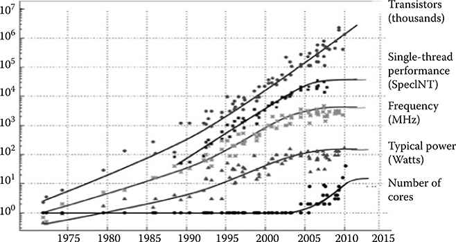
FIGURE 1.1 Microprocessor trends over the past 35 years. (Naffziger, S., Technology impacts from the new wave of architectures for media-rich workloads, Symposium on VLSI Technology © 2011 IEEE.)
1.2 Why Integrate Central Processing Units and Graphics Processing Units on the Same Chip?
CPU and GPU microarchitecture have evolved over time, though the CPU progressed at a much faster pace as graphics technology came into prominence a bit later than the CPU. Graphics is now getting more attention through games, content consumption from devices such as tablets, bigger sized phones, smart TVs, and other mobile devices. Also, as the performance of the CPU has matured, additional transistors from process shrink are used to enhance 3D graphics and media performance, and integrate more disparate devices on the same die. Figure 1.2 compares a system having a discrete graphics chip with another having a GPU integrated on the same die as the CPU. The benefits of having an integrated GPU are immediately apparent [1]:
Bandwidth between the GPU and the DRAM is increased by almost three times. This improves performance quite significantly for bandwidth-hungry graphics functions.
Power and latency of interconnects between the CPU chip and the GPU chip (of the multichip solution) are reduced.
Data can be shared between the CPU and the GPU efficiently through better programming and memory models.
Many workloads stress the GPU or the CPU and not both simultaneously. For GPU-intensive workloads, part of the CPU power budget can be transferred to the GPU and vice versa. This allows better performance–power trade-offs for the system.
Besides these benefits, the trend of integrating GPUs with CPUs has an important scalability advantage. GPUs are inherently parallel and are known to benefit linearly with density improvements. Moore’s Law is excellent at providing density improvements, even though many argue that the performance and power improvements it used to provide have run out of steam. By integrating GPUs, the scalability of computing systems is expected to be better.
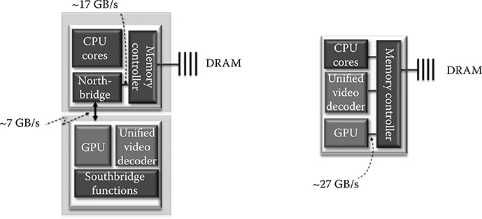
FIGURE 1.2 A multichip central processing unit–graphics processing unit solution (Left). A single-chip central processing unit–graphics processing unit solution (Right). (Naffziger, S., Technology impacts from the new wave of architectures for media-rich workloads, Symposium on VLSI Technology © 2011 IEEE.)
1.3 Case Study of Integrated Central Processing Unit–Graphics Processing Unit Cores
In this section, we describe two modern processors, AMD Llano (Advanced Micro Devices, Sunnyvale, CA) and Intel Ivy Bridge (Intel, Santa Clara, CA), which have both integrated CPUs and GPUs on the same die. These chips are often referred to as accelerated processing units (APUs).
1.3.1 AMD Llano
The AMD Llano chip was constructed in a 32-nm high-k metal gate silicon-on-insulator technology [2]. Figure 1.3 shows the integrated die that includes four CPU cores, a graphics core, a unified video decoder, and memory and input/output (I/O) controllers. The total die area is 227 mm2. CPU cores were x86 based, with 1 MB of L2 cache allocated per core. Each CPU core was 17.7 mm2 including the L2 cache. Power gating was aggressively applied to both the core and the L2 cache to minimize power consumption. A dynamic voltage and frequency system (DVFS) was used that tuned supply voltage as a function of clock frequency to minimize power. Clock frequency was tuned for each core based on power consumption and activity of other CPU cores and the GPU. This was one of the key advantages of chip-level CPU and GPU integration—the power budget could be flexibly shared between these components based on workload and activity.
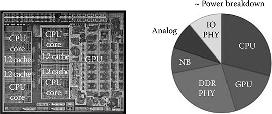
FIGURE 1.3 The 32-nm AMD Llano chip and a breakdown of its power consumption. IO PHY and DDR PHY denote interface circuits for input/outputs and dynamic random-access memory, respectively, and NB denotes the Northbridge.
The GPU used a very long instruction word (VLIW) core as a basic building block, which included four stream cores, one special function stream core, one branch unit, and some general purpose registers. Each stream core could coissue a 32-bit multiply and dependent ADD in a single clock. Sixteen of these VLIW cores were combined to form a single instruction, multiple data (SIMD) processing unit. The GPU consisted of five such SIMDs, leading to a combined throughput of 480 billion floating point operations per second. Power gating was implemented in the GPU core as well, to save power. The GPU core occupied approximately 80 mm2, which was nearly 35% of the die area. Power consumption of the GPU was comparable to that of the CPU for many workloads, as shown in Figure 1.3. The CPU cores and the GPU shared a common memory in Llano systems, and a portion of this memory could be graphics frame buffer memory. Graphics, multimedia, and display memory traffic were routed through the graphics memory controller, which arbitrated between the requestors and issued a stream of memory requests over the Radeon Memory Bus to the Northbridge (Figure 1.4). Graphics memory controller accesses to frame buffer memory were noncoherent and did not snoop processor caches. Graphics or multimedia coherent accesses to memory were directed over the Fusion Control Link, which was also the path for processor access to I/O devices. The memory controller arbitrated between coherent and noncoherent accesses to memory.
1.3.2 Intel Ivy Bridge
Ivy Bridge was a 22-nm product from Intel that integrated CPU and GPU cores on the same die [3]. The four x86 CPU cores and graphics core were connected through a ring interconnect and shared the memory controller. Ivy Bridge had 1.4 billion transistors and a die size of about 160 mm2. It was the first product that used a trigate transistor technology.
Figure 1.5 shows the system architecture of Ivy Bridge, where a graphics core occupied a significant portion of the total die. All coherent and noncoherent requests from both CPU and GPU were passed through the shared interconnect. The shared ring interconnect provided hundreds of GB/s bandwidth to the CPU and GPU cores. The last level cache is logically one, but physically distributed to independently deliver data.
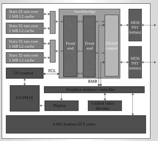
FIGURE 1.4 Block diagram of the AMD Llano chip. FCL denotes Fusion Control Link, MEM denotes memory, PHY denotes physical layers, and RMB denotes Radeon Memory Bus.
In Llano, coherent requests from the GPU went through a coherent queue and the noncoherent requests directly went to the memory. In Ivy Bridge, the CPU and GPU could share data in the bigger L3 cache, for example. The CPU could write commands to the GPU through the L3 cache, and in turn the GPU could flush data back to the L3 cache for the CPU to access. Also, the bigger L3 cache reduced memory bandwidth requirements and hence led to overall lower power consumption. Two different varieties of GPU cores were developed to serve different market segments. The graphics performance is mainly determined by the number of shader cores. The lower end segment had eight shader cores in one slice, whereas the next level segment had two slices. Different components of the processor were on different power planes to dynamically turn on/off the segments based on demands to save power. The CPU, GPU, and system agent were on different power planes to dynamically perform DVFS.
1.4 Technology Considerations
The fundamentally different nature of CPU and GPU computations places interesting requirements on process and device technology [1]. CPUs rely on using high-performance components, whereas GPUs require high-density, low-power components. This leads to the use of performance-optimized standard cell libraries for CPU portions of a design and density-optimized standard cell libraries for GPU portions of a design. For example, the AMD Llano chip had 3.5 million flip-flops in its GPU, but only 0.66 million flip-flops in its CPU. The CPU flip-flops required higher performance and so were optimized differently. The flip-flop used for CPU cores occupied 50% more area than the flip-flop used for GPUs. The need for higher performance in CPU blocks led to the use of lower threshold voltages and channel lengths in CPU standard cell libraries compared to GPU ones.
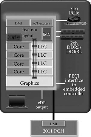
FIGURE 1.5 Block diagram of the Intel Ivy Bridge chip.
The need for higher density in GPUs also leads to the requirement for smaller size wires than a pure-CPU process technology. Smaller size wiring causes more wire delay issues because wire resistivity increases exponentially at smaller dimensions. This is because of scattering at sidewalls and grain boundaries of wires as well as the fact that the diffusion barrier of copper occupies a bigger percentage of wire area.
In the long term, the differences in technology requirements for CPU and GPU cores could lead to 3D integration solutions. This would be particularly relevant for mobile applications where heat is less of a constraint. CPU cores could be stacked on a layer built with a high-performance process technology, whereas GPU cores could be stacked on a different layer built with a density-optimized process technology. DRAM could be stacked above these layers to provide the high memory bandwidth and low latency required for these systems. Figure 1.6 shows a schematic of such a system.
1.5 Power Management
Most workloads emphasize either the serial CPU or the GPU and do not heavily utilize both simultaneously. By dynamically monitoring the power consumption in each CPU and GPU, and tracking the thermal characteristics of the die, watts that go unused by one compute element can be utilized by others. This transfer of power, however, is a complex function of locality on the die and the thermal characteristics of the cooling solution. The efficiency of sharing is a function of where the hot spot is and will vary across the spectrum of power levels. While the CPU is the hot spot on the die, for example, a 1 W reduction in CPU power could allow the GPU to consume an additional 1.6 W before the lateral heat conduction from CPU to GPU heats the CPU enough to be the hot spot again [1]. As the GPU consumes more power, it finally becomes the hot spot on the die, and the reverse situation occurs. A power-management system that maintains repeatable performance must have sophisticated power-tracking capability and thermal modeling to ensure maximum compute capability is extracted from a given thermal solution. Once that is in place, a chip with a CPU and a GPU can deliver far more computation within a thermal envelope than either design in isolation.
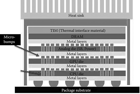
FIGURE 1.6 Three-dimensional integration of central processing unit and graphics processing unit cores. (Naffziger, S., Technology impacts from the new wave of architectures for media-rich workloads, Symposium on VLSI Technology © 2011 IEEE.)
1.6 System Architecture
With the integration of CPU and GPU, there are a few possible system architectures, ranging from separate CPU/GPU memory to a unified one. Until recently, before CPU and GPU were on the same die, the CPU and GPU had their own memory, and data was copied between these two memories for operation. AMD’s road map shows progression from separate physical memory to hardware context switching for GPUs, wherein the chip will be able to decide which of its heterogeneous cores would best fit needs of a particular application [4]. In 2011, AMD partitioned the physical memory into two regions, one each for CPU and GPU. The CPU paging mechanism was handled by hardware and operating system (OS), whereas the GPU paging was handled by the driver. AMD plans to add unified memory address space for CPU and GPU and then add hardware context switching for the GPU. Intel in 2011 used an on-die unified memory controller for CPU/GPU, including sharing the last level cache between CPU and GPU. The on-die GPUs also have different levels of caches similar to CPU for texture, color, and other data.
The data transfer speed and bandwidth between CPU and GPU are critical for performance, and hence a scalable interconnect between these disparate cores is an important factor in APU design. Intel uses a ring interconnect to communicate between many CPU cores and the GPU. In addition to the interconnect design, other considerations in system architecture design include cache organization in both CPUs and GPUs, number of cache levels in the hierarchy, cache sizes at each level, cache policies, and sharing the last level cache. AMD APU (Llano) uses two levels of CPU cache (L1 data cache is 64 KB, L2 cache is 1 MB 16-way) in each of four cores. There is no L3 cache and the memory controller is shared between the CPU and the GPU. In contrast, Intel’s Sandy Bridge has L1 data cache of 32 KB, L2 of 256 KB in each of four CPU cores, and inclusive L3 of 8 MB shared between four CPU cores and GPU using ring interconnect with common memory controller behind the cache hierarchy. The decision to selectively determine the type of data to be cacheable/uncacheable and coherent/noncoherent between the CPU and the GPU can improve performance and bandwidth between cores in both types of system architecture design. Also, general purpose GPU (GPGPU) programming can take advantage of both the integrated cache and the memory controller design to tap into computing power of GPUs. The bandwidth between key units in the system dictates the overall system performance.
1.7 Programming and Memory Models
Hardware manufacturers and software companies have been providing and supporting many tools and new languages to help parallel programming. These tools have evolved since the days when CPU and GPU were separate. First, let us look at a few tools provided by hardware manufacturers. We will then compare them with language extensions and standards proposed from Microsoft to write programs that support multicore CPUs, APUs, GPGPUs, and heterogeneous devices.
Compute Unified Device Architecture (CUDA) (Nvidia Corporation, Santa Clara, CA): In early 2000, a few computer research labs built GPGPU application programming interfaces (APIs) on top of graphics APIs to enable and support GPGPU programming, and two such languages were BrookGPU and Lib Sh. CUDA is Nvidia’s approach to the GPGPU programming problem that lets programmers easily off-load data processing to GPUs [5]. The language is C with Nvidia extensions that provide interfaces to allocate GPU memory, copy data from host to device memory and back, and declare global and shared scope variables, to name a few. First the data has to be copied to the GPU memory before GPU computation is invoked by the CPU, and the results are copied back to main memory after GPU computation. The speedup is based on how efficient the programmers code the parallelism. The CUDA architecture has evolved and it currently supports many high level languages and device-level APIs such as Open Computing Language (OpenCL) and DirectX (Microsoft, Redmond, Washington). The integration of CPU and GPU on the same die will help ease memory bandwidth constraints.
OpenCL: This is a standard that provides a framework to parallelize programs for heterogeneous systems [6]. Programs written using OpenCL can not only take advantage of multiple CPU cores and GPU cores but also can use other heterogeneous processors in the system. OpenCL’s main goal is to use all resources in the system and offer superior portability. It uses a data and task parallel computational model and abstracts the underlying hardware. Data management is similar to CUDA, where the application has to explicitly manage the data transfer between main memory and device memory.
Hardware Multicore Parallel Programming (HMPP): CUDA and OpenCL require programmers to rewrite their code in new language. HMPP, on the other hand, provides a set of compiler directives that supports multicore parallel programming in C [7]. It is a flexible and portable interface for developing parallel applications that can use GPU and other hardware accelerators in the system. The HMPP directives divide the program into multiple codelets that can be run on multiple hardware accelerators. The HMPP runtime handles the parallel execution of the codelets, which have been translated earlier into vendor programming model either by hand or with an available code generator. When the same code is run on a different system, the runtime HMPP will try to find the specified hardware accelerator and run it. If the specified accelerator is not available, the codelet will run on the host core. The HMPP directives also handle transfer of data between host memory and hardware accelerator memory. The HMPP model can also take advantage of shared memory systems like APUs and use fully synchronous execution between CPU and GPU. HMPP also supports Message Passing Interfaces and can run the codelet on a remote host with automatic generation of memory transfers.
Accelerated Massive Parallelism (AMP): Microsoft’s C++ AMP extension allows programmers to express data parallelism as part of the C++ language and lets compilers and DirectX tools create one binary and run on any heterogeneous hardware that supports it to improve performance [8,9]. The C++ AMP understands if the data has to be copied to the GPU based on the memory model and is transparent to the programmer.
The complexity of programming CPU, GPU, and other accelerators is that memory models are different ranging from weak, nonuniform memory access, and so on, from a hardware perspective to a software-managed memory model and recently proposed unified memory model for CPU/GPU and heterogeneous processors. The C++ AMP programming model is progressive looking and works well with AMD’s Heterogeneous System Architecture (HSA) road map that plans to support programming and memory models to support efficient programming of APUs.
Graphics Core Next (GCN): AMD’s GCN is a new design to make GPUs capable of doing compute tasks equally well. AMD is moving from VLIW graphics machine to non-VLIW or SIMD machine as a basic block for GPU. In the new SIMD compute-unit-based GPU, AMD plans to support high level language features such as pointers, virtual functions, and support for GPU to directly call system services and I/O. Also, the new graphics architecture can serve all segments. In the client segment, the new architecture provides similar power/performance as a VLIW machine. And in the server segments, the SIMD basic block with the right software tools can be used as an efficient compute engine and also take advantage of integrated CPU and GPU. The APUs will also provide a view of unified memory between both CPU and GPU to make the data communication efficient by eliminating copying of data between host and accelerator memory that is required in CUDA or OpenCL.
HSA: As the demand to use GPU for purposes other than graphics has been increasing, the GPU architecture is also evolving to support both graphics and compute engine. Also, there is an increased need of software support to use GPUs as compute engines in parallel with other asymmetric cores in the system. HSA provides an ecosystem to build a powerful system from combining simple, efficient, unique, and disparate processors. AMD plans to support coherent and unified memory for CPU and GPU and then provide GPU context switching in future products. The HSA road map is to move from physical integration, architectural integration, and finally to system integration. The architectural integration supports unified address space, pageable system memory for GPU and then fully coherent memory between CPU and GPU. The system integration provides preemption, context switching, and quality of service. AMD’s plan is to treat GPU as a first-class core and give equal privileges as CPU cores with HSA. Currently, AMD is positioned well with their commitment and support to hardware, architecture, and OS tools, and applications for HSA framework and ecosystem.
In summary, there are three main vectors in heterogeneous computing: Instruction Set Architecture (ISA), memory model, and programming model, which covers different memory models and ISAs. We can see that CUDA, OpenCL, HMPP, and C++ AMP target the programming model vector; Graphics Compute Next targets the ISA vector, whereas APUs themselves define the underlying memory model. Another important secondary vector and effect of memory model and programming model is data synchronization. The data synchronization between asymmetric cores depends on the memory model supported by hardware and the one used by the application. As more parallelism is exploited by different accelerators and hardware that support many core counts, the cost of synchronization increases probably to a point where the cost may exceed the benefit of result from parallelism. We know that graphics cores use high memory bandwidth. In a system with APUs, if this high bandwidth traffic from GPU is coherent with the CPU cores, then the snoop bandwidth to all the CPU cores will be high, which will not only increase power and reduce performance of CPU cores but also increase the latency of GPU core. So, an efficient synchronization mechanism becomes important as we move toward programming APUs and future heterogeneous systems. As the potential for parallelism is increased, memory consistency restrictions on hardware may limit the performance.
1.8 Area and Power Implications in Accelerated Processing Units
The area dedicated for graphics is increasing as mobile and desktop devices are demanding more media and graphics performance. In AMD’s Llano APU, GPU occupies around 35% of the die area, whereas Intel’s Sandy Bridge GPU occupies 20% of the die area. Also, the frequency at which the GPU operates is increasing and is taking more percentage of the total power budget, and hence efficient power management is required to increase the battery life. There may come an inflection point, where bigger control units like thread scheduler, dispatcher, scoreboard logic, register file management, and other control units will become a bottleneck and adding more parallel execution units in the GPU may not provide the expected benefit. Similar to the multicore CPUs, instantiation of multiple GPU units is a possible solution. But, the management of two GPU cores has to be supported by drivers and this opens up new challenges for driver management.
1.9 Graphical Processing Units as First-Class Processors
GPUs have matured over time and have powerful graphics and compute engine capabilities. Also, programmers have many options to program APUs, and the tools range from language extensions and declarations/annotations in the programming language to aid compilers and low-level APIs with good debugging tools. Recent trends are to use onboard GPU clusters, networked GPU clusters, and GPU virtualization along with CPU clusters for many applications and creation of clouds and personal cloud networks. All these techniques still use CPU and device driver handshakes to communicate data between host and device memory. Though the GPUs are used for diverse purposes and applications, complete integration of CPUs and GPUs is missing due to lack of framework, standards, and challenges in making this happen. To extend GPU support to the next level, the OS needs to treat GPUs as first-class hardware for complete integration of CPUs and GPUs in the APUs.
To understand the requirements and challenges in making the GPU a first-class processor from the OS perspective, let us briefly look at the current method of interaction between the OS, applications, and CPU and GPU hardware. The main application runs on the CPU and fills up system memory with required information for graphics processing. The graphics part of the main application uses OpenCL, CUDA, or any other previously described programming model API to communicate with the device driver. The device driver in turn will send GPU commands to a ring buffer that acts as a queue to the underlying GPU hardware. Current GPU schedulers mostly use First In, First Out process scheduling that assumes a run-to-completion model and does not preempt tasks for intelligent scheduling. Some of the basic requirements for an OS like preemption and task migration are not supported in the current generation of GPUs.
Figure 1.7 captures the previously described flow between the main application running on CPU that uses system memory and device drivers to run the graphics application on graphics hardware. Recent architectures allow the CPU part and the graphics part of the main application to share information directly in system memory that is transparent to the OS. The drivers, CPU, and GPU part of the application take care of data transfer between cores and coherency.
The number of shader cores and other necessary blocks are increased to handle more data and make the GPU more powerful. There comes a point where just increasing the number of cores may not be easily achieved; instead, adding another GPU core would be easier and complexity-effective. When the number of GPUs has to be increased, the system architecture has to be redesigned. One solution is to add intelligence at the device driver level. Another solution is to add preemption for GPUs and provide control to the OS and treat GPUs as first-class processors [10–12]. With the addition of GPUs, the OS needs to take GPU execution times, resources, migration of GPU tasks, and other information into consideration to come up with new scheduling strategies accordingly. Also, the OS needs to consider different underlying architectures and binaries that will affect the way programs are loaded and dynamically linked. Another challenge is the migration of an already started task from CPU core to GPU core for acceleration will require saving the states from CPU cores and migrating it to GPU cores. Current GPUs provide support for indirect branching to make calls and save state information during exceptions. These primitives and support for shared virtual memory and unified address space proposed in future GPUs are steps in the right direction to make GPUs first-class processors from both a programmer and an OS perspective.
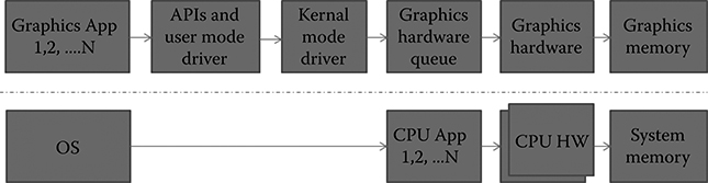
FIGURE 1.7 Interaction between operating system, central processing unit, and graphics processing unit to run graphics application.
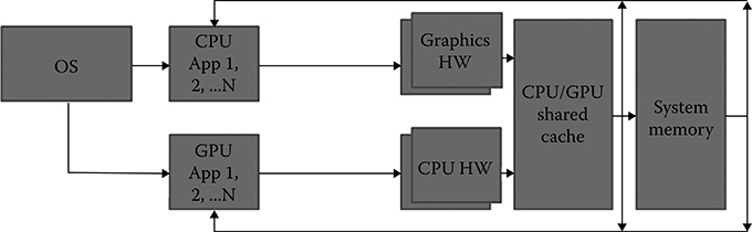
FIGURE 1.8 The operating system treats both central processing units and graphics processing units as first-class processors.
Figure 1.8 shows a future ecosystem, where CPUs and GPUs can communicate through a shared cache and shared memory system. The OS schedules the workloads to both CPUs and GPUs and treats them as equals.
1.10 Summary
Moore’s Law has made the integration of CPUs and GPUs on the same chip possible. This has several important implications for process technology, circuit design, architecture, programming, and memory models, as well as software tools. In terms of process technology, GPUs prefer slower but higher density libraries compared to CPUs, and require smaller size wires as well. This leads to separately optimized process technologies for CPU and GPU portions of a chip, and could eventually lead to 3D integration solutions where CPU and GPU portions of a chip can be stacked atop each other. Power budgets can be efficiently shared between CPU and GPU portions of a design based on thermal and power delivery considerations. Different memory sharing models and interconnect networks are possible for chips that integrate CPUs and GPUs, and performance can be quite sensitive to these decisions. Currently, there are different programming models based on memory models, ISAs, and synchronization mechanisms with high overhead. These constructs will ease the programming model and also help define simpler memory models that help portability and programmability of APU programs. Unified address spaces, preemption, task migration, and other constructs will enable the OS to treat GPUs as CPUs in the long term.
References
1. Naffziger, S. Technology impacts from the new wave of architectures for media-rich workloads, Symposium on VLSI Technology, pp. 6–10, IEEE, Honolulu, HI, June 2011.
2. Branover, A., D. Foley, and M. Steinman. AMD fusion APU: Llano, Micro, pp. 28–37, IEEE, 32(2), 2012.
3. Damaraju, S., V. George, S. Jahagirdar, T. Khondker, R. Milstrey, S. Sarkar, S. Siers, I. Stolero, and A. Subbiah. A 22 nm IA multi-CPU and GPU system-on-chip, Proceedings of International Solid State Circuits Conference, IEEE, San Francisco, CA, 2012.
4. Rogers, P. The Programmer’s Guide to the APU Galaxy, AMD Fusion Developer Summit (AFDS) Keynote, 2011.
5. Nvidia. What is CUDA, http://www.nvidia.com/object/cuda_home_new.html.
6. Khronos Group. Developer Overview, http://www.khronos.org/developers.
7. Wikipedia. OpenHMPP, accessed April 4, 2012, http://en.wikipedia.org/wiki/OpenHMPP.
8. Microsoft Developer Network. C++ AMP (C++ Accelerated Massive Parallelism), accessed April 4, 2012, http://msdn.microsoft.com/en-us/library/hh265137(v=vs.110).aspx.
9. Kanter, D. Adaptive clocking in AMD’s steamroller, Real World Technologies, May 6, 2014, http://realworldtech.com/page.cfm?ArticleID=RWT062711124854.
10. Kato, S., K. Lakshmanan, Y. Ishikawa, and R. Rajkumar. Resource sharing in GPU-accelerated windowing systems, Proceedings of the IEEE Real-Time and Embedded Technology and Applications Symposium, pp. 191–200, IEEE, Chicago, IL, 2011.
11. Kato, S., S. Brandt, Y. Ishikawa, and R. R. Rajkumar. Operating systems challenges for GPU resource management, Proceedings of the Seventh International Workshop on OSPERT 2011, Porto, Portugal, pp. 23–32, 2011.
12. Beisel, T., T. Wiersema, C. Plessl, and A. Brinkmann. Cooperative multitasking for heterogeneous accelerators in the Linux Completely Fair Scheduler, Proceedings IEEE International Conference on Application-Specific Systems, Architectures, and Processors (ASAP), pp. 223–226, IEEE Computer Society, Santa Monica, CA, September 2011.