
6 Soft-Error Mitigation Approaches for High-Performance Processor Memories
Lawrence T. Clark
Contents
6.1.1 Static Random-Access Memory/Cache Circuits
6.1.2.1 Charge Collection Physics
6.1.2.2 Circuit Cross-Section Measurements
6.1.2.3 Static Random-Access Memory Single Event Effect
6.1.3 Mitigating Single Event Upset in the Cache Hierarchy and its Impact on Latency
6.2 Radiation Hardening by Design Level 1 Cache Design
6.2.2 Circuit Design and Operation
6.2.3.1 Cache Error Detection Circuits
6.2.3.2 Single Event Upset Error Checking in the Periphery Circuits
6.2.3.3 Error Checker Area Impact
6.2.4 Measured Speed and Power
6.2.5 Single Event Effect Hardness
6.2.5.1 Single Event Effect Testing
6.2.6 Performance Implications
6.3 Error Detection and Correction
6.4 Register File Hardening and Design
6.4.1 Radiation Hardening by Design Dual Modular Redundant Register Files
6.1 Introduction
Radiation-hardened microprocessors for use in aerospace or other high-radiation environments [1] have historically lagged behind their commercial counterparts in performance. The RAD750 (BAE Systems Inc., Arlington, VA), released in 2001 on a 250-nm rad-hard process, can reach 133 MHz [2]. Recent updates of this device to a 150-nm process have improved on this, but only marginally [3]. This device, built on a radiation-hardened process, lags in part due to the difficulty in keeping such processes up to date, for relatively low-volume devices [4]. The SPARC AT697 (Atmel Corp., San Jose, CA) introduced in 2003 has an operating frequency of 66 MHz, uses triple modular redundancy (TMR) for logic, and error detection and correction (EDAC) and parity protection for memory, soft-error protection [5,6]. More recent radiation hardened by design (RHBD) processors have reached 125 MHz [7]. In contrast, unhardened embedded microprocessors contemporary to these designs achieve dramatically better performance on similar generation processes. For instance, the XScale microprocessor, fabricated on a 180-nm process, operates at clock frequencies over 733 MHz [8]. Ninety-nanometer versions of the XScale microprocessors achieved 1.2 GHz [9] with the cache performance being even higher [10]. More modern designs, such as those in 32-nm cell phone system on chip (SOC) devices, are multicore, out-of-order microprocessors, running at over 1.5 GHz [11]. As portable devices have become predominant, power dissipation has become the overriding concern in microprocessor design. The most effective means to achieving low power is clock gating, which limits circuit active power dissipation by disabling the clocks to sequential circuits such as memories. In caches and other memories, this means that the operation of clocking and timing circuits must also be protected from radiation-induced failures, including erroneously triggered operations.
6.1.1 Static Random-Access Memory/Cache Circuits
Modern microprocessors and SOC ICs have numerous embedded memories ranging in size and access time requirements. Examples include small fast register files (RFs) comprising the data RF, the write buffers, translation look-aside buffers (TLBs), and various queues. These RF memories, with capacities ranging from 1 to 3 kB, often have access times under 500 ps. Single-cycle Level 1 (L1) caches are possible with very aggressive circuit design [12]. Because of the tight timing constraints and the need for fine write (byte write) granularity, EDAC has been infrequently used in commercial microprocessor RFs or L1 caches, due to the deleterious impact it has on the access time. Larger arrays benefit from EDAC with essentially no performance cost with appropriate pipelining, for example, the L2 caches in Ricci et al [9].
Caches are small, fast SRAM memories that allow any address to be mapped to them, enabling the cache to simulate the full memory, but with greatly improved access time. Cache memory is actually composed of two logically distinct (and usually physically distinct) memory arrays—the tag and data arrays as shown in Figure 6.1. Each entry in the tag array holds a portion (the tag) of the memory address, so that the location of the data held in the cache can be found by comparing the tag to the memory address requested. Each tag entry has a corresponding block or line of associated data that is a copy of the memory residing in the corresponding address location. The block or line size generally ranges from four to sixteen words of memory. To access the cache, the tag memory is accessed and if the value stored in memory matches the address, a cache hit is signaled and the associated cache data array value is returned. Otherwise, a cache miss is asserted. In this case, the needed data is fetched from the main memory or the next hierarchical cache level.
L1 caches nearest the core must return data in one, or more usually, two clock cycles. To accomplish this, the tag and data are read out simultaneously in what is known as a late-way-select architecture. The tag comparison (indicated by the question marks in Figure 6.1) determines if one of the tags match the requested memory address. The logical OR of these comparisons indicates a hit, that is, the program referenced memory location does reside in the cache. The match signal selects the data from the correct way to be read out, via the way multiplexer. The number of ways determines the associativity. With an associativity of one (direct-mapped) only one location in the tag and data arrays can hold an address. Greater associativity reduces conflicts for these locations. Power and latency increase with associativity, making this a key trade-off. L1 caches typically have associativities of one to four, although high associativity caches have been used, particularly in low power designs [8].
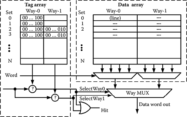
FIGURE 6.1 Architectural view of a two-way set associative cache memory. The data array organization can be different, with separate arrays for each word. This moves the word multiplexing between arrays.
6.1.2 Soft-Error Mechanisms
Single event effect (SEE) is the general term describing device failures due to impinging radiation that deposits charge in the circuit upsetting the circuit state. Depending on the incident particle, devices, and circuit types, there can be different failure modes from the collected charge. These range from benign to catastrophic, but the focus of this chapter is on those that cause soft errors, that is, circuit state upsets that do not permanently damage the circuit. The primary collection mechanisms are drift, charge funneling (a drift-based mechanism), and diffusion (Figure 6.2). The drift components are very fast, whereas diffusion is slower. Charge deposited in the space-charge or depletion region (dashed outline in the inset of Figure 6.2a) is rapidly collected toward the P–N junction by drift. N-type diffusions collect electrons and thus drive the node low, whereas P-type diffusions collect holes and drive the node high. An important prompt collection mechanism is charge funneling whereby the ion track distorts the electric field lines, and allows collection by drift beyond the nominal depletion regions [13]. Diffusion is the least important collection mechanism, because it is slower and diffuses the charge across more collecting nodes. Being slower, it is less likely to overwhelm the driving circuit. Nonetheless, it is clearly responsible for some upset mechanisms and significantly contributes to multiple node collection (MNC) and multiple bit upset (MBU) [14].
The actual waveform is highly dependent on the amount of charge deposited as well as the driving or restoring circuit, which must remove the deposited charge. In the case of a latch, the deposited charge may be sufficient to upset the bistable circuit state, a charge amount termed the Qcrit of the latch, causing a single event upset (SEU) [15]. In this case, the restoring circuit is turned off. For combinational circuits, the effect is termed a single event transient (SET) that can inadvertently assert signals or be captured as machine state when sampled by a latch [16,17]. During an SET, as the collecting node is driven to the supply rail, the diode is no longer at a favorable voltage to collect charge until sufficient charge has been removed by the driver. Some charge may recombine, but due to long lifetimes in modern Si substrates, it tends to linger in a manner analogous to a diode’s diffusion capacitance [18]. Consequently, the SET may be prolonged. In Figure 6.2, the P-type metal–oxide–semiconductor (PMOS) transistor provides its maximum current, IDSAT(P), until sufficient deposited charge has been removed so that the N-type metal–oxide–semiconductor drain diode current is less than IDSAT(P). At this time, the transient of the circuit output node at or near VSS, transitions back to VDD. The resulting voltage pulse (the SET) may cause erroneous circuit operation, particularly in dynamic circuits.
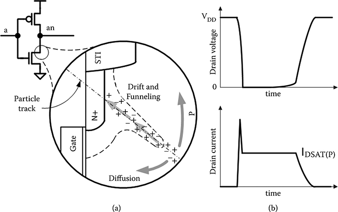
FIGURE 6.2 (a) Soft-error mechanisms and (b) their impact on circuit behavior. A particle impinging on the N-type metal–oxide–semiconductor drain produces a negative voltage glitch (single event transient) whose recovery time is a function of the restoring current provided by the P-type metal–oxide–semiconductor transistor.
6.1.2.1 Charge Collection Physics
An ionizing particle can generate charge through direct ionization, whereby the particle loses energy through columbic interaction with the Si lattice. The energy loss rate is related to the material stopping power dE/dx or linear energy transfer (LET) of the material that it is passing through. The LET is given by
in 1 μm of track length, which is approximately 10 fC of charge per micron of track length per MeV·cm2/mg of LET. Note that a 32-nm technology generation transistor has less than 1 fC of total capacitance per micron of gate width. Charge collection is at diodes, so electrons are collected by N-type diffusions and holes by P-type diffusions. In a bulk complementary metal–oxide–semiconductor (CMOS) process, the latter are in N-type wells of limited depth, reducing the charge due to collected holes.
Angled strikes may allow more charge to be collected at a circuit node (Figure 6.2). The effective LET, LETeff, is given by
where θ is the angle at which the particle strikes the die with 0° being orthogonal to the surface. Originally, LETeff explained greater charge collection at a single node when the particle incidence deviated from normal. Because modern junctions can be very small, the charge track may cross under many sensitive nodes, leading to more separate nodes collecting charge, for example, MBUs. In these cases, LETeff may not be appropriate.
In spacecraft, commonly occurring heavy ions can have LETs up to about 50 Mev·cm2/mg. In Earth orbit, protons are a much greater threat. Until recently, protons have caused soft errors primarily through indirect mechanisms. If the proton undergoes an inelastic collision with a Si nucleus, alpha or gamma particles may be emitted, or a spallation reaction where the nucleus is fragmented may occur [19]. Protons may produce enough charge through direct ionization to be of importance in highly scaled, for example, sub-65-nm devices, where the Qcrit can be as low as 0.3 fC. For example, highly scaled SRAMs have been shown to be susceptible to upset due to direct ionization by low-energy protons [20].
In terrestrial environments, the primary causes of soft errors are alpha particles and neutrons. Efforts to mitigate soft errors in terrestrial systems have transitioned over time from those caused by alpha particles to those caused by high-energy neutrons, as materials used in packaging and fabrication have been reduced in alpha emissivity to fluxes below 0.001 α/cm2/hr. Most terrestrial neutrons pass through the IC without interacting with the circuits, but a small fraction of them interact. When the neutron energy exceeds the necessary threshold energy, nuclear reactions may occur, producing Al and Mg ions that have significant LET. The neutron energy threshold for 28Si + n → p + 28Al is roughly 2.7 MeV, and for 28Si + n → α + 25Mg is around 4 MeV. Beyond 15 MeV, nuclear reactions tend to create more charged ions like 28Si + n → 24Mg + α + n. The charged aluminum (Al) and magnesium (Mg) ions generally travel short distances but produce a large charge deposition. Process improvements to mitigate neutron-induced SEEs include removing borophosphosilicate glass (BPSG) as an intermetal dielectric. BPSG that has a high 10B concentration and 10B has a high neutron-capture cross-section. When absorbing a neutron, 10B splits into a 1.5 MeV alpha particle and a lithium nucleus.
6.1.2.2 Circuit Cross-Section Measurements
ICs are generally ground tested in neutron, proton, or ion beams to determine their susceptibility to SEE. The probability of hitting a target is measured by its apparent target size or cross-section in units of area, given by
where fluence is measured in particles/cm2. The primary goal of SEE mitigation is to limit the errors and hence the apparent cross-section. For heavy ions, the cross-section is typically plotted versus LET using a Weibull fit. The onset of errors is defined as the threshold LET and the saturation cross-section occurs where essentially every particle above that energy is likely to cause an upset. Note, however, that half of the time the type of collection may drive the node to the same logic state that it is already in, for example, N-type diffusions driving a node at VSS low have no impact.
6.1.2.3 Static Random-Access Memory Single Event Effect
Many different latch designs have been proposed to mitigate SEU. The most common approaches are based on the dual interlocked cell that uses circuit redundancy—storage nodes are duplicated, and if only one node is upset, the latch self-corrects [21]. However, as noted previously, ionizing particle deposited charge may be collected by multiple junctions. As fabrication process scaling pushes circuit nodes closer together, spacing the redundant nodes sufficiently far apart, so that multiple redundant circuit nodes are not upset by one impinging particle, increasingly makes using these techniques in SRAM cells impractical. In these MNC cases, the charge is collected by multiple SRAM cells—two or more physically adjacent bits are upset at the same time creating an MBU [22]. Heavy ions and neutrons have been shown to readily produce MBUs [23,24]. Figure 6.3 shows measured SRAM array upsets due to broad beam ion irradiation, with a large proportion of the upsets comprising MBUs. The likelihood that a strike generates an MBU is dependent on the stored data pattern and the ion incident angle, with grazing angles obviously creating the most upsets as the deposited charge is through or near more collecting nodes. Consequently, recent SRAM hardening work has increasingly focused on using EDAC rather than hardening individual cells. It is thus important that the SRAM design interleave storage cells belonging to the same word or parity group, so that MNC does not cause an MBU in the same word. SRAM designers have generally used at least four-cell interleaving to accomplish this and 65-nm data show this continues to be effective [24].
McDonald et al. observed decades ago that SETs in SRAM decoders and control logic could cause upsets that are nonrandom and thus not amenable to mitigation using EDAC [25]. This issue has been observed in SRAMs hardened by process as well, where resistor-hardened SRAM cells exhibited no static errors, but did exhibit dynamic (operating) errors at relatively low LET [26]. These errors can cause the wrong word line (WL) to be asserted, causing a silent data corruption (SDC) error as the parity or EDAC bits read out may match the data. Figure 6.3 also clearly shows one row completely upset. This is due to an SET-induced WL assertion, which wrote the bit line (BL) values into the cells selected by that WL. Mavis et al. reported local WL mis-assertions in an SRAM with hierarchical WLs [27]. Other SET-induced errors can include writes to multiple cells or writes from read-out cells to others, in the case where a WL glitches on after the BLs are fully driven but before BL precharging occurs. Simply increasing driver size and node capacitance has been suggested to mitigate SET [28]. However, experimental measurements of the sizes required, and analysis of larger (merged) SRAM array sizes shows that this may be largely impractical [29].
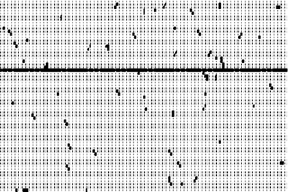
FIGURE 6.3 Measured multibit upsets in a 90-nm static random-access memory. Inset shows example of specific failure patterns. The diagram is taken over time. However, each set of errors has an associated time stamp. Each multiple bit upset is due to a different particle. The upset row is due to a single event transient–induced word line mis-assertion, which wrote the bit line state to the inadvertently selected row.
6.1.3 Mitigating Single Event Upset in the Cache Hierarchy and Its Impact on Latency
Memories make extensive use of dynamic circuits. Dynamic circuits are more prone to upset—each dynamic circuit is a (half) latch, and as described later can thus catch a voltage transient. Consequently, cache SEE mitigation is difficult, as well as critical to the overall microprocessor hardness. In a cache, SEUs may alter the processor architectural state and SETs can cause inadvertent operations, either of which can produce an unrecoverable error or worse, SDC. Moreover, the hardening must be accomplished without adding substantial circuit delay or power. Generally, cache access time limits the microprocessor frequency and caches have accounted for as much as 43% of total embedded microprocessor power dissipation [30]. Although clock gating is the most effective means of limiting power dissipation, some hardening techniques can make clock gating difficult or impossible [31], and the clocks themselves may be inadvertently asserted by SETs [32,33]. Therefore, memory hardening must comprehend the possibility of clock mis-assertions, as well as other types of circuit errors.
L1 caches, that is, those closest to the core itself, most often use the late-way-select architecture shown in Figure 6.4, where multiple tag and data locations are accessed in parallel. The late-way-select scheme also hides the TLB delay, which occurs during the tag set decode and read times. This series TLB/cache tag compare allows the cache tags to use physical, rather than virtual addresses. Note that the decoders receive a portion of the address that is not mapped by the TLB, that is, the cache is virtually indexed.
For SEU protection, L1 caches often use only parity protection, which requires less latency to calculate and facilitates handling byte writes (by having a parity bit per byte). Using an error correcting code (ECC) for cache data, EDAC requires much larger granularity to be efficient; it is usually applied to an entire line. Thus, for EDAC, the existing data must first be read, the write data inserted, and the ECC is recalculated before the actual write. This requires multiple clock cycles and requires additional write buffering for L1 caches. In L2 caches, this is usually the case. In addition, the original data must have its ECC checked and any errors must be corrected before inserting the write data. Memory (and cache) data comprises processor architectural state—a corruption can catastrophically affect program operation. In a cache, which is composed of many subarrays in both the tag and the data storage blocks, as apparent in Figure 6.4, many other potential SET-induced errors can occur, including mis-assertion of the comparators or on the way select circuits, in addition to the SRAM-specific errors in decoders and or sense amplifiers and write circuits.
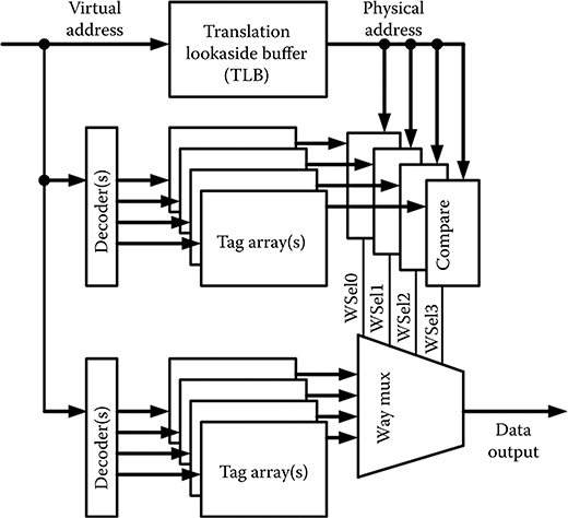
FIGURE 6.4 Four-way set associative L1 cache memory array and circuit organization. Separate tag and data arrays can be accessed simultaneously (there may be more than four, and one array can contain more than one way’s data or tag). The late way select design allows time for the virtual to physical address translation by the translation look-aside buffer before comparing the tag values. The arrays are indexed using address bits within the page, which are not mapped by the translation look-aside buffer, that is, are the same for both virtual and physical addresses.
L2 caches typically access the tag first, and then only the array or multiple arrays that actually hold the data, to save power. The greater latency is tolerable, because the L2 cache is accessed only on an L1 cache miss. Moreover, significant latency is unavoidable—large L2 caches require pipeline stages just to allow for signal delay through on-chip wiring, for example, the L2 cache in Ricci et al. [9] has an eight core clock-cycle latency. A write-through cache simultaneously schedules a write to the main memory (or next level cache) when writing. A write-back (WB) cache only writes data to the main memory when data is deallocated. The latter minimizes bus utilization while a write-through cache can be protected from soft errors by parity checking rather than EDAC, because there is a redundant copy of the data in the next level of the memory hierarchy. In the event of a parity error, the L1 cache line can be invalidated and the good copy will be reloaded from the (presumably ECC protected) main memory when next requested.
6.2 Radiation Hardening by Design Level 1 Cache Design
6.2.1 Cache Organization
This section presents a cache designed to provide hardness by detecting SEE-induced errors. The scheme allows the write-through cache to be invalidated when an error is detected, avoiding potentially otherwise undetectable errors propagating to the processor architectural state. The 16 KB cache is four-way set associative, and uses write-through and no-write-allocate policies [34,35]. Write-through operation allows the cache to employ parity checking. Thus, it does not require EDAC in the timing critical path. When the cache is invalidated on an error, it naturally reloads the data on subsequent misses. In this cache design, in addition to parity errors due to SEU, invalidation can also be triggered by peripheral circuit errors caused by SETs. Alternatively, a software handler can invalidate only the corrupted entries, but this does not significantly improve performance, as shown later. Stores are not gated by the tag hit. Stores perform a tag lookup in the cycle where the write is scheduled. On a hit, the data array write is subsequently executed when there is a free cache cycle. A one entry write buffer delays holds the data until the free cycle occurs.
The cache supports four basic operations: lookup, read, write, and global cache invalidation. Global cache invalidation simply clears the dual redundant valid bits in the tag array. This occurs when the cache is reset, or can be used to rapidly invalidate the contents when a cache SEE-induced error is detected. The dual redundant valid bits are in separate data arrays, so that one control signal mis-assertion cannot upset both. Single cycle writes of 8 bits (store byte) up to 128 bits (cache line fill) are supported. The cache is organized as 1024 cache lines, with 16 bytes (four 32-bit words) in each cache line. It is virtually indexed and physically tagged. Single-cycle fills maximize the memory to cache bandwidth, which at one line per clock is up to 16 GB/s at a 1 GHz clock rate.
The tag array and the two data arrays have 176,128 total bits of storage. Key tag comparator and hit circuits are dual redundant. The SRAM cell has the usual six-transistor structure, but is 3.6 times the size of a cell with smaller two-edge transistors drawn on the same logic design rules—this was done to provide total ionizing dose (TID) hardening (TID is beyond the scope of this chapter). The cell is wide and short to increase critical node spacing, reducing the probability of an MBU affecting the same parity group.
6.2.2 Circuit Design and Operation
6.2.2.1 Circuit Design
Where possible, the hardened L1 cache tag and data arrays use identical circuits and layout cells, that is, the tag array circuits are mostly identical to those in the data array. The data array is split, with the most significant 18 bits of four words on the left and the least significant 18 bits of the same words on the right [36]. In each half data array, there are four words, with four banks for each word. A subbank contains thirty-two 72-bit rows as shown in Figures 6.5 and 6.6. Two subbanks share sense and write circuits, which are between them. There are two bytes, two WLs, and two ways in a data array row. The bit line swing is full VDD to 0 V, so no sense amplifiers are required—NAND gates are used. This lack of a requirement for replica-timed sense amplifier enable signals and no BL multiplexer selects reduces the number of signals that may cause erroneous memory array operation due to SETs. The major data array circuits include the WL decoder, SRAM cell arrays, precharging circuits for the local subarray BLs, and global bit lines (GBLs) which act as the high speed output bus and multiplexer, the write control, and way multiplexer, as shown in Figures 6.5 and 6.6.

FIGURE 6.5 Recent radiation hardening by design cache tag array circuit architecture. There are 16 SRAM cells on each bit line to speed up the way selection signal timing. The 16-cell bit line groups are stacked with the top feeding through the bottom SRAM cells. The tag banks drive dynamic differential domino global bit lines, that are compared to the differential virtual addresses from the TLB. Differential signals ensure that there is no circuit race between the TLB and tag array.
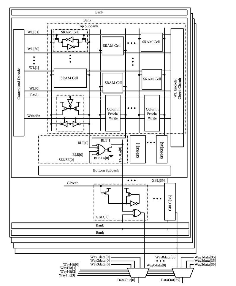
FIGURE 6.6 Recent radiation hardening by design data array circuit architecture. Ways 0, 1, 2, and 3 are interleaved. In the data array sub-bank, there are 32 SRAM cells on each bit line—the tag must be faster as the timing critical path is through the selects. There are two data arrays, each providing 36 bits (LSB array shown).
Since the tag critical timing path through the comparators is limiting, making this path faster is beneficial. To this end, the tag array has 16 cells per BL, by using coincident BLs in a 32-cell column, whereas the data arrays have 32 cells per BL (Figure 6.5). This does, however, increase the peripheral circuit height, as each BL pair requires its own precharge and write circuits, as shown. The tag uses differential reads (Figure 6.5), whereas the data array reads are single ended (Figure 6.6). Both shorter BLs and differential readout reduce the tag read delay, improving the cache access time. The former nearly halves the delay from WL assertion to sense amplifier output. The latter eliminates one inversion delay and allows the one falling edge to the comparators to begin the compare in what would otherwise be a timing race.
6.2.2.2 Performance
Simulated cache circuit operation and critical path timing are shown in Figure 6.7. The timing critical path includes all the circuits that perform the address lookup in the cache. The access begins with the subbank clock assertion (top waveform). The BL and GBL precharge signals are deasserted to allow the BL readout to proceed. The WL decoder then asserts one WL high in banks that are selected (implicitly) by a gated clock assertion. The WL decoder resides after the clock, providing maximum time for address generation in the previous pipeline stage. The tag WL is asserted coincident with the data WL (not shown). One side of the high skew NAND4 BL sensing gates in the tag path drives the GBL pull down transistor on, driving the GBL low, as its complement GBLn stays high. Three of the four dynamic comparators miss and thus discharge, finishing the way selection. The GBLs of the top four banks and bottom four banks associated with each way pair are combined by a NAND2 gate (see Figure 6.6). The static way multiplexer selects the data from the way that hit in the tag array for output. A static way multiplexer is required because all the dynamic comparators precharge to the hit condition. The final output (data out) from the cache way select multiplexer is 830 ps after the rising edge of clock that instituted the operation.
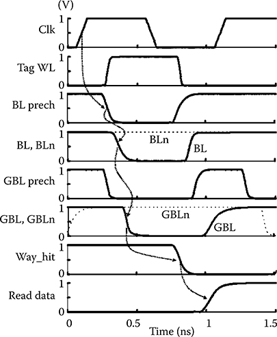
FIGURE 6.7 Simulated recent radiation hardening by design cache critical timing path simulation from clock to read data out. The data array timing is not shown as the critical path is through the way selection signals (buffered versions of WayHit[x]) to the way multiplexers.
6.2.2.3 Power Dissipation
Beside radiation hardness, low power is another primary goal in the cache design. The design is divided into 32 data and 32 tag subbank halves receiving individually gated clocks. The gated clocks dramatically reduce the overall cache activity factor—a sub-bank is activated only when needed, with a maximum of one tag and four data subbanks active for a fill operation, and eight active for a load operation. Clocks are hardened as described in Chellapa et al. [33]. Additional clocks drive the central tag comparator circuits and data array output latches. The WL decoders minimize the address line capacitance and dissipate negligible power in unselected banks. Finally, the cache layout minimizes wire lengths, improving both propagation delays and power dissipation due to signaling. Physically, the tag array resides between the data arrays minimizing the hit signal propagation distance to the data array way multiplexers, and reducing the load (or instruction fetch) power and delay [34]. Redundant tag comparators drive the left and right array way selects, respectively, minimizing the load and delay of each, while allowing checks that determine if one mismatches the other.
6.2.3 Hardening Features
The cache arrays are SEU protected by parity and the bit column interleaving, which for each parity group is maximized by the physical organization. As illustrated in Figure 6.8a, the data arrays use byte parity, which matches the required write granularity. By interleaving bits belonging to two bytes, two WLs, and two ways, the bits belonging to the same parity group (same byte, WL, and way) are interleaved by eight, that is, separated by a distance equal to the width of seven SRAM cells. The tag arrays contain 28 bits per row, using nibble-sized parity groups to maximize the distance, a three SRAM cell separation as shown in Figure 6.8b. The parity is checked on any read values from the data array, but only the hit value in the tag. Any SET-discharged BL or GBL is detected by a parity mismatch. This requires that the critical node spacing of the SRAM cells is carried through all of the cache the column circuits. Alternate groups use even and odd parity. This ensures that a bank that fails to read due to a failed clock assertion will cause a parity error, as all BLs at logic one (VDD) are not a valid output code. Mismatching valid bits constitute one of many detected error conditions.
6.2.3.1 Cache Error Detection Circuits
As mentioned, because an SET can cause an incorrect read or write, the cache uses extensive error detection circuits that monitor potentially erroneous operations due to an SET. These in turn are used to trigger an invalidation operation on the assumption that the architectural state may have been corrupted. The detectors create no new critical timing paths, so the approach taken here allows circuit delays and clock rates that rival unhardened designs. Because SETs are transient, that is, they can dissipate before a sampling clock edge, static checking circuits are inappropriate. The checking circuits are one’s catching, with a set–reset type of operation. The basic dynamic error checker (EC) circuit is based on a domino gate, which as mentioned, with a keeper comprises a half latch—the half latch catches values in one direction. The EC output is subsequently latched locally through a classical dynamic to static conversion, or combined with other error flags, for example, from other memory banks (subarrays), and transmitted to the error control logic where it is latched. An SEE-induced error in the ECs may cause a false error. However, because they compose a very small portion of the cache area, and even in a satellite system, ionizing radiation strikes are infrequent compared to the operating frequency, the impact of both actual and false errors on the overall cache performance is negligible.
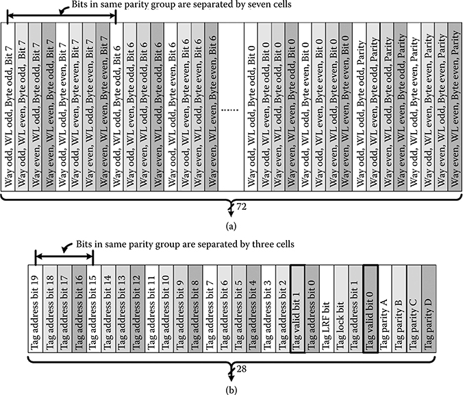
FIGURE 6.8 Physical bit interleaving for (a) data arrays and (b) tag arrays. Bits of the same color are in the same parity group. Spacing is greater in the data arrays, at seven cells between bits in the same parity group. In the tag arrays, the dual redundant valid bits are not included in the parity checks, but a mismatch is indicative of an error.
6.2.3.2 Single Event Upset Error Checking in the Periphery Circuits
Incorrect operations due to a SET that may upset the cache architectural state are protected against by a variety of error checking circuits to detect such events. While BLs are dynamic, and thus prone to SET discharge, the interleaving guarantees that these will result in parity errors so long as the stored data is correct. The focus is on catching control signal, rather than BL errors, although some ECs rely on verifying the correct BL response. Many of the ECs are redundant—a production design may not require all of them, but the research design presented here used the philosophy of better safe than sorry. This section describes some of the WL assertion and BL precharge ECs with illustrations that are exemplary. The other circuits are described.
6.2.3.2.1 Word Line Assertion
If there is a WL error during a write, a write can be missed or data can be written to the wrong row as shown in Figure 6.3. Depending on the array organization, this can also cause the parity or ECC bits to be correct despite the data being incorrect, that is, correct data in the wrong location. To verify correct WL assertion, a dynamic WL encoder is used in each subarray (Figures 6.5 and 6.6) to regenerate the address based on the WL(s) actually asserted (Figure 6.9). The encoded address is subsequently compared with the input (cache set) address. A simple encoding comparison would catch a single WL mis-assertion but cannot detect all multiple WL mis-assertions. For example, an erroneous assertion of WL1 = 000001, would be masked by a correct assertion of WL3 = 000011 if both occurred. To ensure that all such cases are detected, dual complementary encoders are used. This approach will detect any combination of WL mis-assertions. Referring to Figure 6.9, the WL encoder regenerates the address as output WL_encode[n:0] and complement address WL_encodeN[n:0]. The B address is then inverted and, along with the A address, compared against the original set address. Physically, the encoders are interleaved because a blank in one corresponds to a bit in the other—there are no empty cells in the layout as evident by each BL pull down in the schematic driving the left (actual) or right (complement) versions. The layout structure is very similar to the regular SRAM columns (the pull downs are just the access devices). Because the positive and inverted polarity versions are not complementary, that is, they may not match, individual rather than cross-coupled keepers are used.
Because the cache outputs are dynamically multiplexed, that is, only the accessed bank should attempt to discharge the GBLs, incorrectly asserted WLs in unselected subbanks can also cause errors. This is addressed by the WL NOR checker, also shown in Figure 6.9. The right side of Figure 6.9 is the NOR WL EC that detects WL assertions during the precharge phase. This is the exemplary EC circuit. The high fan-in domino gate is triggered by a timing window, where the keeper half latch catches the error. The timing window duration is the time that PrechgN is asserted. The output is captured for subsequent processing and repair. The EC is explicitly reset to remove the error as shown.
6.2.3.2.2 Bit Line Precharge
Failure to precharge the SRAM BLs will cause the next read to be logically ORed with the previous read data. The BL precharge EC circuit monitors the BL and BLn of each column, from a top or bottom subbank (Figure 6.10). If a precharge assertion is missed due to a SET, one of BL or BLn will remain low during precharge. This condition is detected similarly, with a chopped clock (delayed assertion, but synchronous deassertion) to time the detection at the end of the precharge phase of operation. Figure 6.11 shows simulation of a suppressed BLn precharge being detected. The condition of the precharge failing to deassert in time will cause a timing problem, that is, the read will be slow. If the precharge fails to deassert completely, the read will be snuffed and the read-out data will be all 1’s on the BLs. A similar checker is used to detect this case as well.
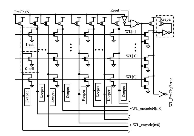
FIGURE 6.9 Word line encoder (left) and NOR checker (right). The encoders are interleaved, that is, layout positions of the transistors match the positions shown here.
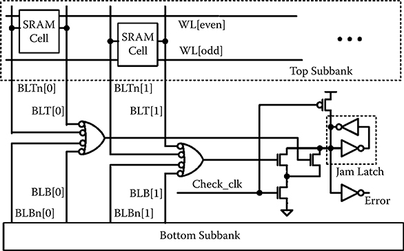
FIGURE 6.10 Local and global bit line precharge suppression detection circuit.

FIGURE 6.11 Simulated bit line precharge mis-assertion and error detection. Prech fails to de-assert in the second clock cycle beginning at 1.5 ns. This in turn, causes the bit line to fail to discharge. The checker detects that neither bit line or BLn discharged on the read and asserts an error.
The write driver is sufficiently strong so that it can override the BL precharge so writes occur correctly if both are simultaneously asserted. However, if the read data is incorrect due to a late or mis-asserted precharge, a single parity polarity will not signal an error in all cases. Consequently, in each word, two bytes use even parity and two bytes use odd parity (one in each side) so that if a read is delayed or fails completely, a parity error occurs.
6.2.3.2.3 Global Bit Line Precharge
The GBL output bus is dynamic as mentioned. Because the subbank read is dynamic, the GBL is a D2 domino bus that lags the local BLs in both read and precharge timing. The GBL precharge can thus be affected by a SET on its precharge control or contention due to a subbank driving its output incorrectly. Two checkers detect errors on the GBLs: one is for the unintended precharge assertions and the other detects failures of the GBLs to precharge, that is, suppression errors.
6.2.3.2.4 Write Bit Line and Enable Assertion
An inadvertently asserted write enable may affect an array that is leaving an accessed state or a reading array by incorrectly writing to it. A WREN and a NOR EC are used to detect these cases. These circuits are similar to that used for the WLs. Because the number of WREN signals is small, encoding is not required. The WREN NOR checker detects errors if any WREN is asserted during the precharge phase. A replica column checks that the BLs were asserted long enough to flip one SRAM cell as well. The cell is reset in each precharge phase.
6.2.3.2.5 Bit Line Read
A number of SET errors can cause incorrect or incomplete BL or BLn signal development. For instance, there may be an unintended short pulse in the BL precharge control signal, or delayed WL development, for example, from a delayed WL enable clock. Any such SET-induced control signal assertion or timing error can cause a delayed, incomplete or incorrect read. These conditions are detected by the read ECs, which reside in each subbank. This EC uses a replica column with a single active SRAM cell that has one side tied to VDD internally, ensuring a read of 0V on the other (single-ended readout) BL. The error condition is signaled if both BL and BLn are high during the check window.
6.2.3.2.6 Tag Compare and Hit Determination
The tag comparators are dynamic so an SET can discharge the comparator domino node. By making these circuits, as well as the hit generation signals dual redundant, they are compared to ensure that any SEE-induced discharge is caught. A multiway hit would result in two ways being selected simultaneously—the merged data from a multiple way selection can have correct parity. Consequently, multiway hits also constitute an error condition. The overhead of the dual redundancy is minimized by using one comparator driver pair for each of the two data memory arrays. Thus, they are each nearly half the size of the one that would be required otherwise.
6.2.3.2.7 Cache Bank Clocks
Cache clock assertions are verified by redundant enables that are checked against actual clock assertions in the clock spine [33].
6.2.3.3 Error Checker Area Impact
The checking circuits comprise 15% of the cache area. This checking-based scheme also allows liberal use of dynamic circuits, which are protected by the checkers or parity. Such circuits are important in high performance cache design, as they allow higher performance in almost every stage, particularly the output busses and the tag comparisons.
6.2.4 Measured Speed and Power
The RHBD cache design has been fabricated on both the standard and low standby power versions of a standard bulk CMOS 90-nm foundry process. The test chip is composed of a cache, programmable test engine, unhardened phase lock loop (PLL), and RHBD clock spine [34]. All test engine circuits, including I/O, are implemented as TMR circuits that self-correct by voting, with the exception of the foundry provided PLL. The PLL is shielded during heavy ion tests. The self-correcting TMR circuits have demonstrated exceptional hardness and thus do not contribute to the measured SEE-induced error rate.
The test chips verify the efficacy of the error checking approaches at speeds up to 200 MHz at VDD = 1.32 V, limited by the test engine circuitry. A test that works around these timing limitations was written to experimentally determine the cache speed. This test demonstrates that the cache data arrays can write and read at 1.02 GHz at 1.3 V. At VDD = 1.45 V, the measured cache power dissipation is 22.8, 25.1, and 26.4 mW at 85.7, 92.3, and 100 MHz, respectively. The standby power on this die is 71 μW. The 1 GHz peak cache power is calculated to be 266.1 mW, by linear extrapolation. At nominal VDD = 1.2 V, the peak cache power dissipation is projected to be 182 mW at 1 GHz at 100% activity factor. In actual operation, stalls and other architectural inefficiencies will make the typical power lower. For a data cache, because loads and stores are about one-third of operations, typical cache power dissipation will be below 0.1 mW/MHz.
6.2.5 Single Event Effect Hardness
6.2.5.1 Single Event Effect Testing
The test die has been exposed to the 15 MeV/u ion beam at Texas A&M University in air at room temperature, with VDD = 1.45 V as well as at the Lawrence Berkeley NL cyclotron with 10 MeV/u ions in vacuum at VDD = 1.2 V. Our previous broad beam SRAM tests on this fabrication process (e.g., used for the SRAM data in Figure 6.3) had shown that high VDD exacerbates multibit upsets. N, Ne, Cu, Ar, Kr, and Au ions were used in the beam tests. Fluences from 5 × 10⁵ to 2 × 10⁷ particles/cm2 were used, adjusted so that high LET MBUs would not overwhelm the 8 k entry field-programmable gate array error recording buffers. The maximum angle was 79° (0° being normal incidence) and the beam was incident on the die front that is, metallization side. The device package shielded part of the cache during those tests, as evident in upset bit maps, so in most tests the maximum angle used was 65°. During each beam test, the programmable test engine exercises the cache with lookups (processor load instructions) and (optionally) store operations at 100% activity factor. When a checking circuit detects an error, the test is interrupted, the reported error is recorded for analysis, and the tag and data array contents are dumped and analyzed to determine the impact of the error on the cache contents. The test is then resumed.
6.2.5.2 Tag Array Results
6.2.5.2.1 Memory Array Soft Errors
The tag array measured cross-sections versus LET are shown in Figure 6.12. Least squares Weibull fits to the incorrect hit/miss response, tag parity error, and valid bit upset are also shown. The bit cell upset errors exhibit a rapid rise and saturation with a uniformly low threshold LET that follows the bit cell cross-section, indicating that most are SEU. Note, however, that a local or global BL discharge will also register as a parity error as mentioned previously. The tag response is dominated by SEUs, with most of them causing an incorrect hit/miss response. Parity protects the lock, and least-recently filled bits as well as the stored line address. To save the power and wire density impact of delivering all tags to external parity check circuitry, only the tag that hits is checked. Because it is very likely that an SEU will change a tag to a value that is not in the test, and parity is only read on tags that hit, most tag SEUs do not cause a parity error.
Tag SEUs can thus strand a line by moving its address outside the program space. In a WB cache, the parity error will be detected on eviction, but the line cannot be written back to the correct memory location. However, the effect in a write-through cache is benign, as the line will be reloaded when the cache misses an access to it. In the event that the post-SEU address resides in an active program, the cache will register a hit. Thus, when the upset tag location is finally read, a parity error will be triggered. Because of their redundancy, an SEU that flips one of the valid bits effectively invalidates the entry. However, the valid bits are split between the dual redundant comparator circuits. Thus, one may hit, if that valid bit is still correct, while the other may miss. The resulting response is a dual redundant hit/way select mismatch error. In this manner, many of the SEE-induced cache errors observed in the tests are correlated.
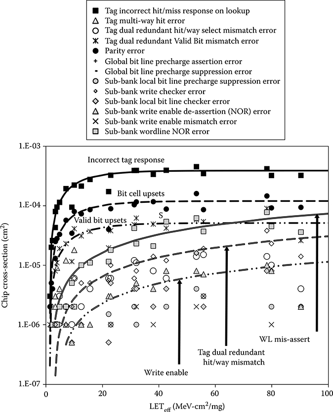
FIGURE 6.12 Tag SRAM array and control error cross-sections with the beam incident in the bit line direction. Parity errors are labeled Bit cell upsets, since they were confirmed by checking the actual data. Saturation cross-section is similar for the word line direction, but with reduced low linear energy transfer cross-section. The small tag array sizes allow control errors to essentially double the cross-section.
6.2.5.2.2 Tag Peripheral Circuit Errors
The SET-induced peripheral circuit errors have very different Weibull fits than SEU in the arrays, exhibiting softer saturation and higher threshold LET. Note, however, that the threshold LET is still low enough to be susceptible to neutron-induced upsets in a terrestrial environment—the primary mechanism for neutron upset is secondary ion generation, with the likely Mg ions generating up to 20 fC/μm of track length. At LETeff = 50 MeV ·cm2/mg, the WL errors have a cross-section about one-tenth of the tag bit SEU. Note that the relatively small, low power arrays have low threshold LET for a number of SET-induced control logic errors. The key result is that for tag arrays, such peripheral errors can contribute significant errors. The cross-sectional data provide quantitative insights as to the SET susceptibility of specific peripheral circuits. For instance, the global BL precharge EC detects few errors, and none at low LET. Moreover, many errors are strongly correlated. This was expected because many are redundant, as mentioned in Section 6.2.3.2. Consequently, depending on the IC hardness goals, some, perhaps most, of the checking circuits can be deleted. By focusing on the most likely errors, that is, WL assertion and write enable should provide sufficient reliability. By using static comparators, which are slower, some dual redundant mismatches can be eliminated, albeit at a negative operating frequency impact.
6.2.5.3 Data Array Results
The data array results in both the WL and BL directions are shown in Figure 6.13. The parity errors coincident with data load mismatches dominate. This can be expected based on the lower relative area and complexity of the peripheral circuits in the data array. The larger data arrays produce a larger cross-sectional gap between the array (SRAM cell) SEU and those due to SETs, because their relative peripheral circuit area is less than in the tag arrays. For the data arrays, no global BL precharge suppression errors were recorded, but incorrect assertion errors were. We surmise these were due to SETs in the relatively small driving circuitry. The precharge devices on these large busses are large and thus their driver cross-section is very small. As in the tag arrays, the most likely SET-induced error was WL mis-assertions. In an actual microprocessor, the root cause of such an error can be an SEU, because any address error will create a WL mis-assertion, and a latch containing the address can be upset at any pipeline stage. However, because the addresses into the cache in the test chip were self-correcting TMR logic, it can be concluded that these errors were within the cache arrays, most probably the decoders. Figure 6.14 compares the data array cross-sections for the angled beam oriented along the array WLs and along the BLs. The slightly lower WL direction SEU cross-sections can be attributed to smaller MBU extent, because cells are further apart in that direction. The Weibull fits show a small, but probably not meaningful difference for the SET-induced WL and write errors.
In most, but not all of the data array mismatches, a parity error was generated. With an MBU span of two, no upsets should escape the parity check. The root cause of these errors was traced to an interaction between the tag and data circuits. In these nonparity error data mismatch cases, tag way/hit mismatches were detected. Because the dual redundant comparators drive the left and right data arrays, respectively, different ways were selected in the separate arrays—each had correct parity. Note that in the case of a single comparator, if its result is erroneous, the chosen data would be returned from the cache with no error reported, that is, an SDC would potentially occur. In the RHBD cache here, this error is caught by the way/hit comparisons of the dual redundant circuits and the SDC avoided. Only one clock spine error was reported by the device under test during a store and lookup test using Au, with an angle of 53°, the beam along WL direction at LETeff = 152 MeV·cm2/mg. Because the clock assertion is gated to control whether a subbank should fire and subbanks may be writing, this requires action to avoid potential state corruption. Importantly, the ion beam experiments showed that all array errors are caught—no cache state was ever upset without triggering an error.
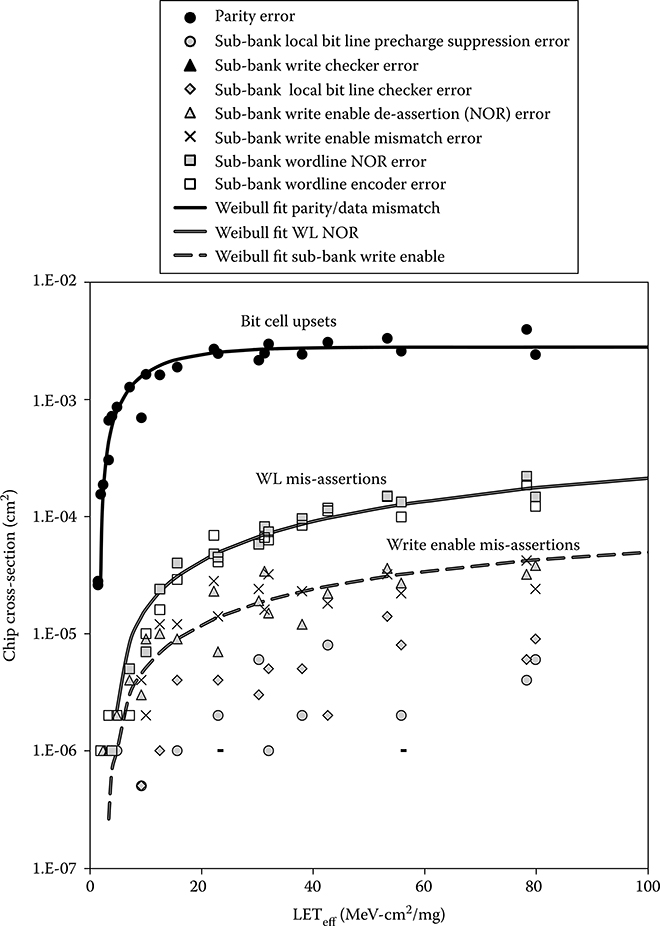
FIGURE 6.13 Recent radiation hardening by design cache data array and control error cross-sections with the beam incident in the bit line direction. Word line write enable mis-assertions dominate the control errors, although nearly all checkers did detect errors.
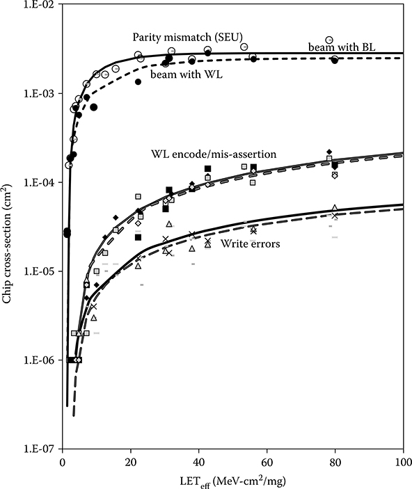
FIGURE 6.14 Recent radiation hardening by design Cache data array and control error cross-sections with the beam incident in the bit line direction (solid lines) and the word line direction (dashed lines). The higher cross-section in the bit line direction is due to more words being affected since the spacing is closer and there are no intervening N-wells. Cross-sections for control errors have little or no dependency on the beam direction.
6.2.6 Performance Implications
The strategy employed for the RHBD write-through cache is to invalidate the contents whenever one of the ECs detects a SET-induced signaling error, so it cannot affect the processor architectural state. With this approach, a memory scrub is just a read of each location. Although it is likely that many of these invalidations are unnecessary, this approach avoids error escapes. In general, SEEs are rare events compared to the clock rate, even in the worst-case orbital conditions. For example, in geostationary earth orbit, the average time interval between particles that hit the cache and having an LET greater than 1 MeV·cm2/mg is calculated to be 3000 seconds or 50 minutes. Operating at a clock rate of 1 GHz, with a 10 core clock miss penalty and a 95% cache hit rate, the performance impact is well below 0.0001%.
6.3 Error Detection and Correction
The most commonly used ECC is based on Hsiao codes [37] which add r check bits for every group of k data bits forming a k + r bit code word. A single error correction, double error detection code requires all legal code words to be at least four bit changes apart, that is, they have a Hamming distance of four. Codes capable of correcting multiple bit errors are starting to be used in L2 and L3 caches as they protect not only against MBUs, but also against sporadic bit failures, for example, bits that pass IC testing but become unstable over time. Before the data is written into the memory, the check bits are calculated and subsequently stored with the data. When data is read, the check bits are recalculated and exclusive ORed with the stored check bits to generate a syndrome code that is also r bits in length. If all the syndrome code bits are zero, then no single or double bit error has occurred and the data is assumed to be correct. Note that this may not be true—if enough bits have been upset to transform one legal code word into another, then an SDC has occurred. The syndrome is decoded to point to the incorrect bit, which is inverted. The primary cost of EDAC is that it generally requires a read, modify, and write cycle to insert data into a code word. L2 caches nearly always have such a buffer, but small embedded microprocessors rarely do.
L1 caches generally support byte writes for a store byte instruction commonly used in string operations. The hardened SPARC processor design in Gaisler [38] uses a (32, 7) BCH code for multibit error correction. This design is very slow, but even then double writes incur an extra clock cycle. In a high performance microprocessor L1 cache, this latency impact is unacceptable, because a pipeline stage must be added to the load/store operations. Moreover, this process must be implemented in a relatively sophisticated write buffer. An alternative is to add sufficient check bits to each byte so that each code word of data, consisting of the data byte and the check bits, supports EDAC. This implies greater than 50% memory overhead.
6.3.1 Memory Scrubbing
EDAC and other parity-based schemes, with the proper column interleaving, can provide excellent SEU mitigation. However, they must be protected from upsets in the same code word due to multiple particles. The mean time to failure is given by
where M is the memory bank size, t is the interval between scrubbing operations, C is the number of code words in each bank, B is the number of memory banks, and λ is the bit failure rate. Even in orbital applications, low scrub rates are required—on the order of hours between scrub operations can be sufficient. A write-through cache can be periodically flushed because as mentioned, periodic cache invalidation is equivalent to a scrub, and is supported in a single clock cycle in the RHBD design presented here. The detection scheme here limits the invalidation performance impact, while mitigating this SDC risk.
6.4 Register File Hardening and Design
Because of the high performance required, microprocessor RFs commonly use parity protection, which is fast to generate, but can only allow soft-error detection. The Itanium server microprocessor incorporated parity in a unique low overhead scheme that does not add to the critical timing path, albeit at the cost of a few unprotected cycles [39]. A key problem in RF soft-error protection is the lack of time in the pipeline, that is, critical timing paths, for EDAC calculation in the stages leading to and from the RF. Mohr presented a sufficiently fast XY parity-based EDAC scheme to allow its use in RFs [36]. In addition, EDAC does not protect against erroneous data or operations caused by SETs, either in the RF or in the arithmetic logic unit (ALU)/bypass circuitry that produces and consumes data residing in the RF. Analysis of synthesized RFs on a 90-nm CMOS process showed that adding EDAC for each nibble incurred at minimum a 34% speed impact while saving only 45% the area required for TMR. For large 32- and 64-bit registers encoded as a single ECC code word, an extra pipeline stage was necessary [40]. This is unacceptable in a high performance processor.
6.4.1 Radiation Hardening by Design Dual Modular Redundant Register Files
The RHBD RF design described in this chapter combines microarchitectural and circuit level approaches, starting with dual mode redundancy (DMR) for compatibility with a DMR data path. DMR decoders generate redundant read and write WL signals [41]. Full SEE protection is provided by DMR combined with large critical node separation through bit interleaving and parity. The DMR data path is not essential; however, Ditlow, in work contemporaneous with design presented in this section, showed that DMR storage allows excellent RF SEU protection [42]. However, no SET protection was provided by Ditlow’s design.
Like the RHBD cache, in this RF design, parity provides error detection. DMR allows one copy to provide clean data for SEU corrections; interleaving prevents multicell upsets (MCUs) from causing uncorrectable errors; and again, inadvertent operations are prevented by circuit approaches. The parity protection is in 5-bit groups to provide the greatest possible node spacing to mitigate MNC. A standard load-store CPU has two read ports and one write port, supporting the two ALU operands and single result, respectively. This design adds a third, that is, the Rt/Rd read port used to read a copy of the destination register contents about to be overwritten in the next cycle WB pipeline stage (see Figure 6.15). This extra port allows overwritten RF data to be restored when an error condition is detected. There are two basic ECs: in the first the DMR data are compared; the store is cancelled due to a detected data path error (SEU or SET) that is detected as the WB is in progress (the WB checker is labeled A vs. B data comparison in Figure 6.15). The second EC detects write word line (WWL) mis-assertions by the WWL checking circuit, shown in Figure 6.16 and described in detail in Section 6.4.1.1. DMR does not indicate which copy is erroneous, so the original (pre-WB pipeline stage) data are returned to the RF and then the instruction with nonmatching results is restarted from the beginning of the pipeline after the RF is checked for SEUs and those are repaired.

FIGURE 6.15 DMR register file configuration showing read and write port connections, including feedback to the Rt/Rd write port for error correction using data in the copy with correct parity to overwrite data in the other copy with a parity error. Correction is by nibble, so bits in both register file entries can be upset so long as both copies of any nibble are not. Mismatches in the A and B write-back data are caught on the input to the RF, stalling the processor to restart with a clean architectural state. (L. Clark et al., “A dual mode redundant approach for microprocessor soft error hardness,” IEEE Trans. Nuc. Science, 58[6], © 2011 IEEE.)
6.4.1.1 Circuit Design
Referring to Figure 6.15, the checking circuits are labeled A versus B data comparison, which check that the WB data match. The same checking mechanism is used to detect WWL mismatch errors that occur when one of the two WWL copies is asserted, but not the other. This logic is like that of the cache ECs described previously (see Figure 6.16). Clock chop circuits delay the turn on edge to allow the checked state to settle after the rising clock edge controlling the state transitions. The same delays are used to generate a pulsed precharge, which eliminates the need for a dynamic to static converter latch. The D2 domino ERRA and ERRB signals are discharged for any transient mismatch between the checked inputs. The full keeper (rather than the standard PMOS only keeper in Figure 6.9) holds the state even if the mismatch transient is short, regardless of the clock period.
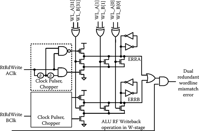
FIGURE 6.16 The dual redundant register file write word line checking circuit. This circuit follows the approach used in the recent radiation hardening by design cache. Pulsed clocks, which create the checking window, require a full keeper on dynamic nodes ERRA and ERRB.
The RF storage cell design is shown in Figure 6.17. The cell differs from that in a conventional dynamic RF in that a write operation requires simultaneous assertion of two redundant WWLs—this mitigates the possibility of inadvertent writes to RF locations due to control logic SETs. The aforementioned checker reports when a WWL deassertion aborts an intended write. When implemented with a DMR control and data pipeline, one WWL, WWLa, is controlled by the A pipeline copy, while WWLb is controlled by B pipeline circuits. Consequently, an SEE manifest as a control error that propagates to the RF from one copy cannot affect the architectural state in the RF. Read out is conventional, discharging the dynamic read bit line (RBL) if the cell state is a logic “1.” Two of the read ports are connected to one side of the cell, and one to the other, to increase the minimum storage node capacitance, which would dominate the cell SEU hardness. When an error occurs, either due to a mismatch of the DMR input data or WWLs, the register that is the target of the write is restored to its prior state—putting back the correct architectural state. Similarly, if one of the WWLs is truncated, which may partially write both copies, the entire operation is started over from the previously correct architectural state. Soft errors manifest as read word line (RWL) errors, if they affect the data read, are corrected similarly.
6.4.1.2 Error Correction
The design is intended to use software-controlled repair mechanisms [41], but the key aspects could be handled by hardware. Basically, once an error is detected, any SEU can be corrected in 64 clock cycles, as 32 two-cycle operations. Each A and B 32-b register copy is read simultaneously; if they mismatch, the A or B nibble with the correct parity overwrites the copy with incorrect parity. Hardware multiplexing paths between the copies carry out these operations. Only accumulated errors affecting the same parity group in both copies result in an uncorrectable error, but due to large physical separation between cells in the same parity nibble these are almost certainly due to separate SEU events, that is, error accumulation.
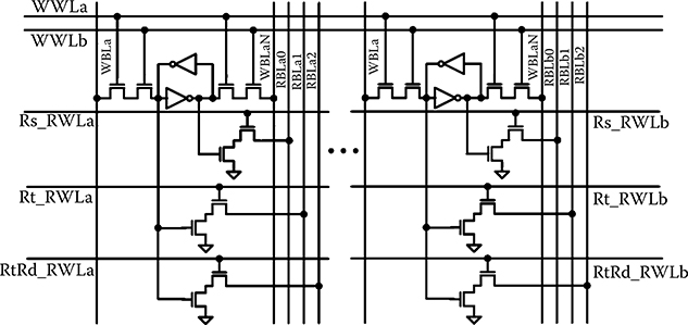
FIGURE 6.17 DMR register file cell circuit showing the read and write ports. The inverting one port allows added capacitance on both sides of the storage cell to increase Qcrit.
Error accumulation is avoided by background scrub operations. Besides allowing potentially incorrect data to be backed out when a mismatch between the A and B data copies is detected, the Rt/Rd read port also allows opportunistic scrubbing. When an instruction will not write to the RF in the WB pipeline stage, it is not a load instruction, the Rt/Rd read port is opportunistically used to read the next register pointed to by a scrub pointer. The read-out value is automatically checked for parity errors. This allows all registers to be sequentially read in a rotating fashion as normal operations occur. The scrubs opportunistically use the Rt/Rd port, when it is not required by an instruction writing back to the RF.
6.4.1.3 Physical Design
The RF layout showing the bit interleaving is shown in Figure 6.18. The decoders are spatially separated, to prevent SEEs from corrupting both copies simultaneously. Like the cache design composing Section 6.2, the bits of each parity group are interleaved to maximize the separation and thus, likelihood of MNC affecting 2 bits in the same parity group. The interleaving allows a spacing between such critical nodes of 16 standard cell heights (greater than 32 μm).
6.4.1.4 Single Event Effect Testing
Two basic broad beam proton and ion tests were performed, static RF and dynamic RF/ALU/bypass tests. The former exercises the RF memory statically, that is, without the data path in operation, to determine the RF SEU and SET characteristics independent of the data path errors. The latter have shown that the DMR RF, when used with a DMR data path and control logic, can effectively mitigate all soft errors at speed, where SETs are prevalent. As in the cache testing, fully self-correcting TMR circuitry is used to test the RF in the test chips.

FIGURE 6.18 DMR register file physical design. Interleaving of the register file columns, where A indicates the A copy, B indicates the B copy, and the number is the bit number in the word.
In the static tests, the RF is written with all 0’s, all 1’s, or a checkerboard pattern. The RF is then read continuously by the test engine using only a single read port. In the event of an error, the upset stored data are corrected and the test continues. Each location is read a second time if there is an error. A SET in the RF dynamic RBL circuits, address, or decoding, is detected if the read data is initially incorrect, but is correct on the second read. Both RF (A and B) copies are tested, which reflects the actual DMR processor operation, where each redundant data path/control copy receives unchecked and uncorrected RF data.
The RF WB checking circuits are used in the dynamic tests to characterize the data path checking functionality. In these tests, a DMR Kogge–Stone adder, complete with input and output bypass paths as used in a standard microprocessor performs arithmetic operations on the RF data. The types of errors generated by the data path can also be examined in this mode. Thus, these tests allow SETs to corrupt many bits in one copy, for example, due to transients on the adder prefix circuitry corrupting the most significant bits—propagating carry errors, or incorrect function selection or data bypassing due to control SETs in one DMR pipeline copy. When an error is detected in these tests, the check type is logged. Moreover, in these tests, parity checking is turned off, so as to propagate more errors into the data path. Referring to Figure 6.15, these types of errors create a WB error indicating the A and B WB data mismatched (A vs. B data comparison in Figure 6.15), or a WWL error, which indicates that the WWL checker found a WWL assertion discrepancy (WWL checking in Figure 6.15) for example, due to different A and B addresses. For these errors, the test engine dumps the RF contents, allowing accumulated RF SEUs to be examined. Finally, the RF is reloaded with correct contents and the dynamic test resumes.
6.4.1.4.1 Heavy Ion Testing Results
Boron, oxygen, neon, argon, and copper broad beam ions with nominal (normal incidence) LET of 0.89, 2.19, 3.49, 9.74, and 21.17 MeV·cm2/mg, respectively at angles ranging from 0 (normal) to 70° were used to test the RF. Testing was primarily performed at 100 MHz and 200 MHz at VDD = 1, 1.2, and, 1.4 V. At angles, the beam was aimed across the words, the direction for which MBUs would be most likely. During heavy ion testing, the PLL clock source was shielded. The RF bit cross-section (Figure 6.19) shows a low threshold LET of approximately 1 MeV·cm2/mg, presumably due to near minimum sized PMOS transistors. However, it is perceptibly higher than the SRAM cells in the cache. We attribute this to the significantly greater capacitance of the multiple read ports, which as mentioned were distributed to both storage nodes. Over 90% of the SEUs were single bits. The largest MNC extent was 2 bits. Over 98% of the static test SETs were detected with logic “1” stored, clearly indicating that the dynamic RBLs dominate the RF SET cross-section.
Chip-level RF cross-sections measured with dynamic testing, for argon ions with nominal (normal incidence) LET = 12.89 MeV·cm2/mg, at 40°beam angle, is shown in Figure 6.20. WB error and WL error refer to how the initial error was detected; SEU refers to other errors inside the RF when the contents were dumped; scrubbing was not run, but writes naturally update some RF contents. The bar labeled WB error indicates that an A/B copy mismatch detection triggered an RF dump. The SEU bars indicate only RF errors that were not the original cause of the detected error, that is, accumulated upsets. WB error MBUs are shown, indicating SETs in the data path are detected. Their prevalence demonstrates the importance of protecting against data path SETs in an RHBD design. The MBU column shows upsets of multiple cells, where two-bit upsets predominated, as in the static tests. However, these can also include the logic fan-out-induced errors mentioned previously.

FIGURE 6.19 Measured register file bit cell heavy ion cross-section determined by static testing at VDD = 1.2 V. (L. Clark et al., “A dual mode redundant approach for microprocessor soft error hardness,” IEEE Trans. Nuc. Science, 58[6], © 2011 IEEE.)
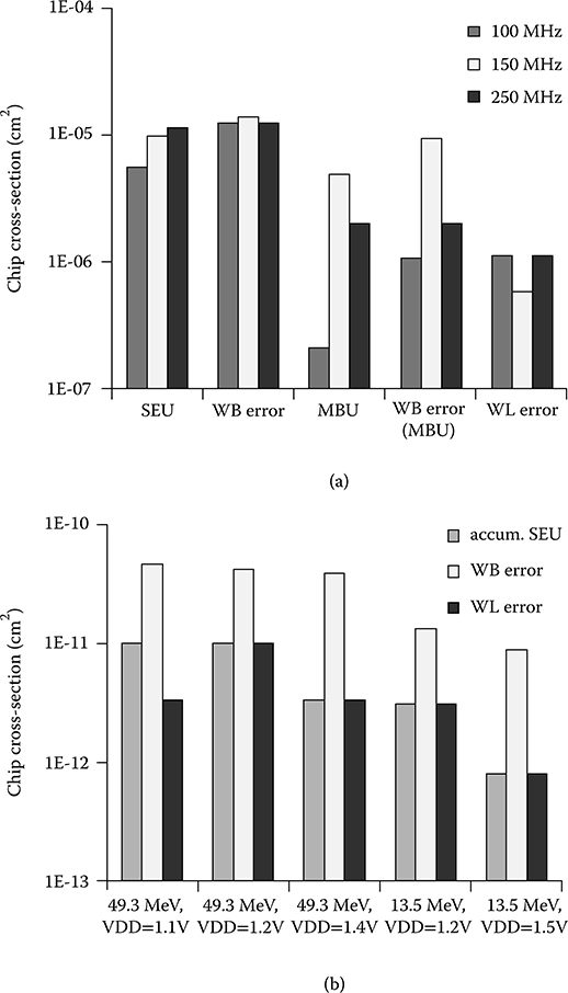
FIGURE 6.20 (a) Measured register file and ALU/bypass circuit heavy ion cross-section from dynamic testing exercising both at VDD = 1.2 V and linear energy transfer = 12.89 MeV/cm2/mg (40° angle). (b) Measured register file and ALU/bypass circuit proton cross-section from dynamic testing exercising both at multiple proton energies and VDD. write-back error and word line error refer to how the initial error was detected; Accumulated SEU refers to other (SEU) errors inside the register file when the contents were dumped. (L. Clark et al., “A dual mode redundant approach for microprocessor soft error hardness,” IEEE Trans. Nuc. Science, 58[6], © 2011 IEEE.)
6.4.1.4.2 Proton Testing Results
Proton beam energies of 49.3 and 13.5 MeV were used. Although tests with the PLL were performed, most of the testing was performed at 60 MHz using the PLL bypass mode, because PLL upsets can cause test chip malfunctions due to bad clocks and the PLL is difficult to shield from protons. For most RF tests, the total fluence was 5(1011) protons/cm2. Flux was 2.3(108) to 8.9(108) protons/cm2/s. For the 49.3 MeV proton energy, the measured cell (per bit) cross-sections for static SEU testing of the RF were 3.71(10−14) cm2, 2.68(10−14) cm2, and 1.12(10−14) cm2 at VDD = 1, 1.2, and 1.4 V, respectively. Similar response was measured for all 0’s and all 1’s patterns, which we attribute to the well-balanced RF cell storage node capacitance. In static testing, SETs were observed only for the read all 1’s case but with a very low cross-section. This is also as expected—N-type diffusions predominate on the BLs, so they are generally pulled in one direction by a SET. For the 13.5 MeV proton beam energy, the measured cell cross-sections for static SEU testing of the RF were 1.07(10−14) cm2, 8.98(10−15) cm2, and 1.72(10−15) cm2 at VDD = 1, 1.2, and 1.4 V, respectively. MCUs were rare and the longest upset extent was 2 bits. Cross-sections VDD supply voltages and proton energies measured in the dynamic tests comprise Figure 6.20b. A modestly reduced cross-section at higher VDD and lower energy are evident.
6.5 Conclusions
This chapter has focused on novel error detection techniques to mitigate soft errors in high speed microprocessor memories such as L1 caches and RFs. A write-through policy allows the former to be invalidated when errors are detected, and the likelihood of errors due to cache control logic was shown to be significant, particularly in the tag memory arrays. The cache approaches have been experimentally proven to be effective, although a reduced EC set may be adequate, reducing the area overhead below the 15% achieved here.
The RF testing data confirm that DMR hardening techniques are effective for mitigating errors in these timing critical memories. SEU MCU extent was far below the critical node spacing achieve by column interleaving. While many bit errors (representing a potentially large equivalent MCU extent) were detected in the dynamic tests, the many bit errors occurred only in one, for example, the A but not B, copy—clearly indicating data path logic error propagation. Regardless, these operations are restarted. The DMR RF provides excellent SEU immunity, and is consistent with commercial designs that have split the RF for performance, rather than for hardening reasons, because the RF read port overhead often dominates that of the storage itself.
Adding ECs to detect errors introduced into or produced by the memory periphery circuits such as sense, write, prechargers, and the decoders has been shown to be effective in mitigating such SET and pipeline latch SEU errors. The EC circuits themselves do not contribute to the circuit critical paths substantially, although mechanisms must be provided to undo some of the side effects of inadvertent operations, for example, the RF writes.
References
1. K. Label et al., “Single event effect proton and heavy ion test results for candidate spacecraft electronics,” Proc. Radiation Effects Data Workshop, 1994, pp. 64–71.
2. D. Rea et al., “PowerPC RAD750-A microprocessor for now and the future,” Proc. IEEE Aerospace Conf., Big Sky, MT, 2005, pp. 1–5.
3. N. Haddad et al., “Second generation (200MHz) RAD750 microprocessor radiation evaluation,” Proc. RADECS, 12th European Conference, Sevilla, Spain, 2011, pp. 877–880.
4. R. Lacoe, J. Osborne, R. Koga, and D. Mayer, “Application of hardness-by-design methodology to radiation-tolerant ASIC technologies,” IEEE Trans. Nuc. Sci., 47(6):2334–2341, December 2000.
5. C. Hafer et al., “LEON 3FT processor radiation effects data,” Proc. Radiation Effects Data Workshop, Quebec, Canada, 2009, pp. 148–151.
6. S. Guertin, C. Hafer, S. Griffith, “Investigation of low cross-section events in the RHBD/FT UT699 Leon 3FT,” Proc. Radiation Effects Data Workshop, Las Vegas, NV, 2011, pp. 1–8.
7. F. Sturesson, J. Gaisler, R. Ginosar, T. Liran, “Radiation characterization of a dual core LEON3-FT processor,” Proc. RADECS, Sevile, Spain, 2011, pp. 938–944.
8. L. Clark et al., “An embedded 32-b microprocessor core for low-power and high-performance applications,” IEEE J. Solid-state Circuits, 36(11): pp. 1599–1608, November 2001.
9. F. Ricci et al., “A 1.5 GHz 90-nm embedded microprocessor core,” VLSI Cir. Symp. Tech. Dig., pp. 12–15, June 2005.
10. J. Haigh et al., “A low-power 2.5-GHz 90-nm level 1 cache and memory management unit,” IEEE Journal of Solid-state Circuits, 40(5):, pp. 1190–1199, May 2005.
11. S. Yang et al., “A 32nm high-k metal gate application processor with GHz multi-core CPU,” ISSCC Tech. Dig., San Francisco, CA, 2012, pp. 214–215.
12. D. Bradley, P. Mahoney, B. Stackhouse, “The 16 kB single-cycle read access cache on a next-generation 64 b Itanium microprocessor,” ISSCC Technical Digest, San Francisco, CA, 2002, pp. 110–111.
13. C. Hsieh, P. Murley, and R. O’Brien, “A Field-funneling effect on the collection of alpha-particle-generated carriers in silicon devices,” IEEE Elec. Dev. Let., EDL-2(4): pp. 103–105, 1981.
14. F. Sexton et al., “SEU simulation and testing of resistor hardened D-latches in the SA3300 microprocessor,” IEEE Trans. Nuc. Sci., 38(6): pp. 1521–1528, December 1991.
15. P. E. Dodd and F. W. Sexton, “Critical charge concepts for CMOS SRAMs,” IEEE Trans. Nucl. Sci., 42: pp. 1764–1771, 1995.
16. M. Gadlage et al., “Single event transient pulsewidths in digital microcircuits,” IEEE Trans. Nuc. Sci., 51: pp. 3285–3290, December 2004.
17. J. Benedetto et al., “Heavy ion induced digital single-event transients in deep submicron processes,” IEEE Trans. Nuc. Sci., 51(6): pp. 3480–3485, December 2004.
18. D. Kobayashi, T. Makino, and K. Hirose, “Analytical expression for temporal width characterization of radiation-induced pulse noises in SOI CMOS logic gates,” Proc. IRPS, Montreal, Quebec, Canada, pp. 165–169, 2009.
19. A. Holmes and L. Adams, Handbook of Radiation Effects, Oxford University Press, New York, 2002.
20. D. Heidel et al., “Low energy proton single-event-upset test results on 65 nm SOI SRAM,” IEEE Trans. Nuc. Sci., 55(6): pp. 3394–3400, December 2008.
21. T. Calin, M. Nicolaidis, and R. Velazco, “Upset hardened memory design for submicron CMOS technology,” IEEE Trans. Nuc. Sci., 43(6): pp. 2874–2878, December 1996.
22. R. Koga et al., “Single ion induced multiple-bit upset in IDT 256K SRAMs,” Proc. RADECS, St Malo, United Kingdom, pp. 485–489, 1993.
23. T. Karnik, P. Hazucha, and J. Patel, “Characterization of soft errors caused by single event upsets in CMOS processes,” IEEE Trans. Secure and Dependable Computing, 1(2): pp. 128–144, April 2004.
24. G. Gasiot, D. Giot, and P. Roche, “Multiple cell upsets as the key contribution to the total SER of 65 nm CMOS SRAMs and its dependence on well engineering,” IEEE Trans. Nucl. Sci., 54(6): pp. 2468–2473, December 2007.
25. P. McDonald, W. Stapor, A. Campbell, and L. Massengill, “Non-random single event upset trends,” IEEE Trans. Nuc. Sci, 36(6): pp. 2324–2329, December 1989.
26. L. Jacunski et al., “SEU immunity: The effects of scaling on the peripheral circuits of SRAMs,” IEEE Trans. Nuc. Sci, 41(6): pp. 2324–2329, December 1989.
27. D. Mavis et al., “Multiple bit upsets and error mitigation in ultra-deep submicron SRAMs,” IEEE Trans. Nuc. Sci., 55(6): pp. 3288–3294, December 2008.
28. Q. Zhou and K. Mohanram, “Gate sizing to radiation harden combinational logic,” IEEE Trans. CAD, 25: pp. 155–166, January 2006.
29. K. Mohr and L. Clark, “Experimental characterization and application of circuit architecture level single event transient mitigation,” IRPS Proc., pp. 312–317, April 2007.
30. J. Montanaro et al., “A 160 MHz 32 b 0.5 W CMOS RISC microprocessor,” IEEE J. Solid-state Circuits, 31(11): pp. 1703–1714.
31. K. Warren et al., “Heavy ion testing and single event upset rate prediction considerations for a DICE flip-flop,” IEEE Trans. Nuc. Sci., 56(6): pp. 3130–3137, December 2009.
32. N. Seifert et al., “Radiation induced clock jitter and race,” IRPS Proc., pp. 215–222, April 2005.
33. S. Chellapa, L. Clark, and K. Holbert, “A 90-nm radiation hardened clock spine,” IEEE Trans. Nuc. Science, 59(4): pp. 1020–1026, 2012.
34. X. Yao, D. Patterson, K. Holbert, and L. Clark, “A 90 nm bulk CMOS radiation hardened by design cache memory,” IEEE Trans. Nuc. Science, 57(4): pp 2089–2097, August 2010.
35. X. Yao, L. Clark, D. Patterson, and K. Holbert, “Single event transient mitigation in cache memory using transient error checking circuits,” Proc. CICC, San Jose, CA, pp. 1–4, 2010.
36. K. Mohr et al., “A radiation hardened by design register file with low latency and area cost error detection and correction,” IEEE Trans. Nuc. Sci., 54(4): pp. 1335–1342, August 2007.
37. M. Hsiao, “A class of optimal minimum odd-weight-column SEC-DEC codes,” IBM J. Res. Develop., 14(4): pp. 395–401, July 1970.
38. Gaisler, J., “A portable and fault-tolerant microprocessor based on the SPARC v8 architecture,” Proc. Dependable Systems and Networks, 2002, pp. 409–415.
39. E. Fetzer, D. Dahle, C. Little, and K. Safford, “The parity protected, multithreaded register files on the 90-nm Itanium microprocessor,” IEEE J. Solid-State Circuits, 41(1): pp. 246–255, January 2006.
40. R. Naseer, R. Bhatt, and J. Draper, “Analysis of soft error mitigation techniques for register files in IBM Cu-08 90nm technology,” Proc. IEEE Int. Midwest Symp. Circ. and Sys., San Juan, PR, pp. 515–519, 2006.
41. L. Clark, D. Patterson, N. Hindman, K. Holbert, and S. Guertin, “A dual mode redundant approach for microprocessor soft error hardness,” IEEE Trans. Nuc. Science, 58(6): pp. 3018–3025, 2011.
42. G. Ditlow et al., “A 4R2W register file for a 2.3GHz wire-speed POWER™ processor with double-pumped write operation,” ISSCC Tech. Dig., San Francisco, CA, 2011, pp. 256–258.