
12 Three-Dimensional Spintronics
Dorothée Petit, Rhodri Mansell, Amalio Fernández-Pacheco, JiHyun Lee and Russell P. Cowburn
Contents
12.2 Topological Kink Solitons in Magnetic Multilayers
12.5 Soliton–Soliton Interaction
12.6.1 Effect of Dipolar Interaction
12.1 Introduction
Spintronics is an emerging technology in which the spin of the electron is used to form a new generation of radiation-hard, nonvolatile, low-energy devices. To date, most interest has focused on memory applications such as hard drive read heads or on future replacements for dynamic random-access memory and battery-backed static random-access memory. In this chapter, we discuss the possibility of using spintronics as a route to three-dimensional integrated circuits. Spintronics is an interesting candidate for three-dimensional architectures because high levels of functionality can be achieved from simple, thin magnetic films without the need for any top contacts or gate electrodes. Furthermore, thin magnetic layers can be easily coupled to each other simply by inserting a carefully selected nonmagnetic material between them. Finally, spintronic devices can usually be designed to minimize thermal dissipation from the magnetic element itself, meaning that power dissipation from the center of a three-dimensional ensemble of elements would not be excessive. These features open up the possibility of stacking highly functional but structurally simple units on top of each other, allowing data to be held, moved, and processed in a vertical direction as well as in the conventional lateral directions.
In this chapter, we present a numerical study of such a three-dimensional spintronic device. In this system, binary data is coded into chiral phase shifts in the anti-parallel (AP) arrangement of antiferromagnetically coupled multilayers (MLs) with well-defined anisotropy. These are localized, stable, and can be controllably and synchronously propagated in the vertical direction of the ML by using an external rotating magnetic field.
Spintronics is a new technology in which the spin of the electron is used to create devices.1 Because the electron spin is most commonly associated with ferromagnetic materials, spintronic devices are usually of a hybrid construction in which ferromagnetic materials such as nickel, iron, and cobalt are integrated into semiconductors. Because ferromagnetism persists even in the absence of any power supply, spintronic devices are usually nonvolatile and as such make excellent memories. Because many of the physical effects that are exploited in spintronics are interfacial effects, magnetic materials are usually found in spintronic devices in thin or ultrathin form usually between 0.6 and 10 nm thick. The nonlinearity of the magnetic hysteresis loops of thin film magnetic materials leads to a wide range of interesting functionalities that stretch beyond simple binary memories, including logic functions2–4 and microwave sources.5 Spintronics is a particularly interesting candidate when it comes to thinking about three-dimensional devices. To date, most three-dimensional complementary metal–oxide–semiconductor (CMOS) devices have been implemented at a packaging level by stacking multiple dies on top of each other. Although the metal interconnect network on a very large-scale integrated device is intrinsically three-dimensional, most CMOS still retains only a single layer of active transistors at the bottom of the devices. Because high levels of functionality can be achieved in a single magnetic layer only 0.6 nm thick, one can begin to imagine three-dimensional devices in which many active layers, each less than a nanometer thick, are fabricated on top of each other using standard ML growth methods. One of the challenges in achieving an enormously high density three-dimensional spintronic device is finding a scheme for coding and transporting digital information between layers. Physical mechanisms such as dipolar interactions6,7 and Ruderman–Kittel–Kasuya–Yosida (RKKY) coupling8 allow neighboring layers of magnetic material to couple to each other from an energetic point of view. The challenge is finding ways of converting that simple physical coupling into a functional information carrying channel. This relates closely to the physics of complex magnetic structures and noncollinear spin textures, which can exist in coupled magnetic system. Understanding these is the route to finding ways of using nearest neighbor interactions to represent and move information.
More fundamentally, complex magnetic structures are the subject of intense research in a variety of fields of condensed matter, from designing magnetically controlled ferroelectric materials9 to chiral magnetic kink soliton lattices10 and skyrmionic matter,11–16 to cite only a few examples. In these systems, the antisymmetric Dzyaloshinsky–Moriya17,18 exchange interaction is a key ingredient to the existence of a noncollinear spin state. Nevertheless, chiral noncollinear structures can arise in systems with symmetric interactions. Magnetic bubbles in thin films19 or disks20 with perpendicular anisotropy are such an example. Frustration induced by the competition between different antiferromagnetic (AF) interactions can also lead to the formation of helical magnetic structures.21–23
In this chapter, we show that AF-coupled magnetic MLs offer the possibility to engineer chiral magnetic textures. A very interesting theoretical24–27 and experimental28,29 body of work showed that a chiral antiphase domain wall can be induced in MLs with an even number of layers by means of surface spin-flop (SSF). However, this chiral texture was found experimentally to disappear in the absence of an applied magnetic field.30,31 Nevertheless, this is an excellent starting point for the engineering of a controllable spin texture that runs in the vertical direction.32 Here we will show numerically that by tuning the ratio of the uniaxial anisotropy to the interlayer coupling in such MLs, it is possible to induce antiphase domain walls—or topological magnetic kink solitons—which are stable at room temperature.33,34 Furthermore, we show that they are mobile and that it is possible to control their propagation using an external magnetic field. Finally, we show how they interact with each other and we discuss their experimental realization. These are the main requirements of an information vector for a three-dimensional spintronic system and so could lead to a dramatic shift in data storage technologies and digital logic devices.
12.2 Topological Kink Solitons in Magnetic Multilayers
Figure 12.1a shows a schematic of a ML made of in-plane magnetic material (light gray) AF coupled through a nonmagnetic spacer layer (dark gray). The strength of the coupling is defined by a coupling field J* = JAF/MStM, where MS is the saturation magnetization, tM is the thickness of the magnetic layer considered, and JAF is the interaction energy. The layers are assumed to have a uniaxial anisotropy Ku (anisotropy field Hu = 2Ku/MS) in the direction indicated by the double arrow. The minimum energy configuration of such a system has adjacent layers AP and pointing along the easy anisotropy axis. There are two equivalent ways of realizing this ground state, as shown in Figure 12.1a, the white and gray arrows show the direction of the magnetization in each layer. We characterize these configurations by calculating the quantity Φn = (−1)ncos (θn), where θn is the angle between the magnetization in the nth layer and the x axis. Φn describes the AF phase of the nth layer, where all the layers in one of the two ground states take either the value + 1 or −1. When these two ground states, or domains, meet, as shown in Figure 12.1b, the magnetization in the two layers on each side of the meeting point (indicated by *) points in the same direction, causing frustration as the AF coupling is not satisfied.
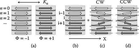
FIGURE 12.1 (a) Schematics of the two antiparallel configurations. (b, c) Meeting of two domains with opposite Φ. (b) Hu > J*, the frustration is sharp and achiral. (c, d) Hu < J*, the frustration is chiral and both layers forming the frustration splay in one of two directions.
If J* is weak compared to Hu, the magnetization in both frustrated layers will point in the easy axis direction despite the AF coupling and the transition area will be sharp (Figure 12.1b); if Hu is weak compared to J*, then both layers will lower the interaction energy at the expense of the anisotropy and splay away from each other, with the transition area extending to the adjacent layers as the coupling increases. This splaying can happen either clockwise (when going through the transition area upwards [Figure 12.1c]), or counterclockwise (Figure 12.1d), defining the chirality of the transition region.
We have performed zero-temperature macrospin simulations using a steepest descent minimization of the energy of the system. In this model, the magnetization is assumed to be uniform across each individual layer i and the total reduced energy density e = E/MSVJ* is:
where θH is the angle between the applied magnetic field and + x, V is the volume of a magnetic layer, h = H/J*, and hu = Hu/J*. Note that e depends only on reduced field parameters.
Figure 12.2a shows the calculated spin configuration across a transition in a stack with hu = 0.5. The magnetization directions are represented as if viewed from the top of the stack, that is, the angles represent the actual deviation of the magnetization in the (x, y) plane. Figure 12.2b shows the evolution of Φn across a transition as a function of layer number n, for hu = 2 and 0.5. For hu = 2 the transition is sharp, that is, Φ goes directly from −1 to +1 between two layers; for hu = 0.5 the transition is gradual. Figure 12.2c shows the width of the transition, defined as the number of layers it takes to go from 10% to 90% of the Φ transition, as a function of hu. For high hu ≥ 1.3 ± 0.1, the transition is sharp and the soliton is achiral. Then, following a sharp rise around hu ~ 1 where the transition acquires a chirality, the width monotonously increases as hu decreases. Figure 12.2d shows the same data as a function of j* = 1/hu.
There is an analogy between these systems and domain walls in soft ferromagnetic nanowires. Both are topologically locked, that is, their existence is a consequence of the conditions at the domains boundaries (topological kink solitons). Furthermore, the size of domain walls also depends on the balance between the anisotropy and the ferromagnetic exchange interaction of the material.35 The discrete synthetic system studied here allows us to directly engineer the anisotropy and the coupling.
12.3 Soliton Mobility
12.3.1 Principle
Propagation of a soliton occurs when one of the two layers at its center reverses: if layer i on Figure 12.1b switches, then the soliton moves one layer up the stack to in-between layer i − 1 and i; if layer i + 1 switches, the soliton moves one layer down. The difference between these two layers at the center of a soliton and layers inside the bulk of a domain (AP state) is that the latter are stabilized on both sides by AP neighbors whereas soliton layers have only one AP neighbor, the other neighbor being parallel (zero interaction field if we neglect the splay between layers at the center of the soliton). They will therefore be the easiest to reverse. Unidirectionality of soliton propagation is imposed by selecting which of these two layers will switch first. For a chiral soliton, this can be achieved using a rotating magnetic field.
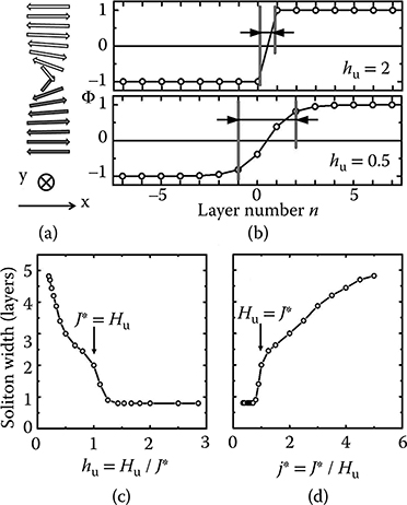
FIGURE 12.2 (a) Macrospin configuration in a stack with hu = 0.5. (b) Parameter Φ for hu = 2 and 0.5. (c) 10%–90% width of the transition region versus hu. (d) Same data as (c) versus j*.
We simulated the application of a global in-plane field of amplitude h = H/J* to stacks containing a single chiral soliton. Snapshots of the spin configuration for hu = 0.5 and h = 1 are shown in Figure 12.3a through j; the field sequence is shown at the bottom of each snapshot (black arrows). The white and gray arrows at the bottom show the magnetization of the two layers at the center of the soliton. The field first increases from zero to h in the + x direction, causing the magnetization in the two layers at the center of the soliton to point closer to the field direction (Figure 12.3b), but still symmetrically about the field. As the field starts rotating, clockwise in this case, this symmetry is broken and the white layer follows the field (Figures 12.3c and d) and switches (Figure 12.3e), becoming part of the bottom gray domain. In Figure 12.3f, the soliton has moved one layer up and the initial symmetry is restored. As the field keeps rotating with the same sense (Figures 12.3g and h), the white layer follows the field and switches (Figure 12.3i), becoming part of the bottom gray domain as well. After a full 360° rotation of the field (Figure 12.3j), the soliton has moved two layers above its original position and the magnetization in the central layers of the soliton points in the initial direction. If the sense of rotation of the field is reversed, the soliton moves in the opposite direction, and for the same rotating sense a soliton with opposite chirality (counterclockwise) moves in the opposite direction (down). It is worth emphasizing that correct soliton propagation happens in discrete steps (two layers per field cycle), which is not the case for domain walls in ferromagnetic nanowires where the shape of the nanowire has to be engineered to impose the synchronization between the applied field and the domain-wall movement.3
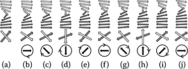
FIGURE 12.3 Macrospin simulations showing the effect of applying a clockwise in-plane rotating magnetic field to a stack containing a clockwise soliton (hu = 0.5, h = 1). The field direction is displayed at the bottom; the middle panel shows the directions of the two layers forming the soliton. Both are shown top–down.
12.3.2 Operating Margin
In the same way that ferromagnetic nanowires are characterized by their field-driven domain-wall conduit properties,36 that is, how easy it is to move domain walls for a substantially lower field amplitude than necessary to nucleate new domains, these ML stacks also have soliton conduit properties. Figure 12.4a and b show a reduced rotating field amplitude diagram illustrating the different possible behavior for a soliton stack. The same set of data is plotted in both graphs—only the normalization factor differs. Figure 12.4a shows a reduced rotating field amplitude diagram h = H/J* for synchronous soliton propagation as a function of hu = Hu/J*. If h is too low (No prop. area below the squares), the soliton does not propagate; if h is too high (Nucleation area above the circles), the barrier constituted by the 2J* stabilizing field in the bulk plus the anisotropy field Hu is overcome and the bulk reverses, erasing the soliton. Synchronous soliton propagation arises in the middle of these two boundaries. However, directional rotating-field-driven propagation of solitons is achieved only for the low field—low anisotropy light gray Correct prop. area below the triangles. We saw in the previous section that to propagate a soliton using a rotating field, the former has to be chiral. Sharp achiral solitons cannot couple to a rotating field. The consequence of this is that solitons in MLs with hu ≥ 1.3 ± 0.1 (i.e., with j* ≤ 0.77) (see Figure 12.2c and d) are not expected to be controllable using rotating fields. A nonchiral soliton layer is still easier to switch than a bulk layer, but the propagation is not unidirectional anymore. Which of the top or bottom layer of the soliton follows the rotating field and switches first is now a consequence of the presence of random defects rather than a controlled process.
The dark gray Non-unidirectional prop. area, however, extends below hu = 1.3 if the applied field is high enough. This is due to the fact that, as illustrated in Figure 12.3b, a magnetic field will pull the soliton layers toward its direction. The field necessary to fully saturate both soliton layers, and thereby erase the chirality of the soli-ton, increases as hu decreases. This is reflected in the triangle line in Figure 12.4a. Above that line, an otherwise chiral soliton becomes achiral and loses its ability to couple to a rotating field and propagate unidirectionally.
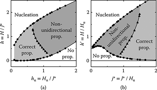
FIGURE 12.4 (a) Rotating field amplitude h = H/J* versus hu = Hu/J* diagram. (b) Same set of data plotted as h′ = H/Hu versus j* = J*/Hu. The light gray area corresponds to synchronous unidirectional propagation, the dark gray area to non-unidirectional synchronous propagation.
Stack edge effects were not included in the calculation of the diagram. Even in the absence of dipolar interactions, the propagation properties of broad solitons (low hu) are affected by the proximity of the edges of the ML. This interaction between a soliton and stack boundaries is of the same nature as the soliton—soliton interaction, which will be discussed later. The calculations were performed on a stack containing enough layers that the properties were independent of the number of layers (50–100). Furthermore, the top and bottom layers were fixed to avoid edge-induced nucleation of domains.
Figure 12.4b shows the same data with a different normalization (Hu) and as a function of j*. This figure will be used in Section 12.6.1.
12.4 Soliton Stability
It is possible to calculate the energy barrier to propagation of a soliton within the macrospin model. For a clockwise soliton (Figure 12.1c), the energy barrier corresponding to forward propagation is obtained by a variational method where the energy of the stack is minimized as layer i is artificially rotated clockwise. This energy is shown in Figure 12.5a (dotted line) for hu = 1 as a function of the rotation angle with respect to the +x direction (the zero-field equilibrium angle for these parameters is indicated by a full dot). The energy increases with the layer angle and reaches a maximum when layer i is pointing along the hard axis. For a stack with Hu = 1300 Oe, hu = 1, MS = 1400 emu/cm3, tM = 1.4 nm (corresponding to Fe on Cr (211) with a Cr thickness of about 1.3 nm)37 and lateral dimensions of 200 × 200 nm2, this barrier corresponds to 72 kBT at room temperature.
To calculate the energy barrier to backward propagation, the energy of the stack is computed as layer i is rotated counterclockwise, the energy profile is also shown in Figure 12.5a (solid line). In that case, the energy first increases as the magnetization of layer i aligns more closely with that of layer i + 1, due to the increase in coupling energy. It reaches a maximum as both layers point in the same direction along the easy axis (corresponding to 1500 kBT at room temperature for the parameters cited previously), then decreases as both layers splay away from each other again. At the minimum (open dot), the chirality of the soliton has flipped from clockwise to counterclockwise. The second leftmost barrier corresponds to backward propagation of a counterclockwise soliton and is identical to the one corresponding to forward propagation of a clockwise soliton.
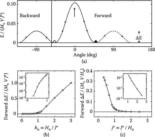
FIGURE 12.5 (a) Energy barrier to forward and backward propagation of a soliton in a stack with hu = 1. The arrow indicates the barrier related to soliton chirality flipping. (b) Height of the forward energy barrier to propagation ΔE/MSVJ* as a function of hu. Inset: same low hu data in a semi-Log scale. (c) Height of the forward energy barrier to propagation ΔE/MSVHu as a function of j*. Inset: same high j* data in a semi-Log scale.
The height of the energy barrier to forward propagation ΔE/MSVJ* is plotted in Figure 12.5b as a function of hu. The inset shows the same data for 0 < hu < 1 with a logarithmic vertical scale to highlight the appearance of a nonzero ΔE. For hu < 0.25 ± 0.05, ΔE is zero; solitons are unstable and any perturbation such as thermal fluctuations or edge effects will expel them from a finite stack. For hu > 0.25 ± 0.05, ΔE increases monotonically with hu. Figure 12.5c shows the same ΔE data, this time normalized by MSVHu.
Unidirectional propagation is ensured by the high energy barrier to chirality flipping. However, when a field is applied, the Zeeman energy tends to decrease the splay between the magnetizations of the two layers at the center of the soliton, that is, this energy barrier to chirality flipping is modified by the presence of the field. The line formed by the triangles in Figure 12.4a shows the boundary above which the energy barrier to chirality flipping goes to zero. Above this line, the field erases the chiral identity of the soliton, so that both layers are equally likely to switch during the subsequent half-field cycle and unidirectional propagation is lost.
It was found in Velthuis et al.30 and Meersschaut et al.31 that the antiphase domain wall obtained after SSF—which is essentially a chiral soliton of the kind that we are describing here—was not stable on reduction of the applied field. This is confirmed by our results. Their system has an hu of less than 0.25; as can be seen in Figure 12.5b, it corresponds to a soliton with a zero propagation energy barrier.
12.5 Soliton–Soliton Interaction
Because solitons of the same chirality propagate in the same direction under the same globally applied field, it is possible to unidirectionally propagate several of solitons in one ML stack. However, solitons in the same ML interact; solitons of the same chirality repel; solitons of opposite chirality attract (and annihilate if close enough). This is illustrated in Figure 12.6 where two solitons of opposite chirality (Figure 12.6a) and of the same chirality (Figure 12.6b) are placed in close proximity in the same stack. When the chiralities are opposite, the system can lower its energy by rotating counterclockwise the layer in-between the two solitons (marked with *) to be more AP to the layers below and above; that is, it is energetically favorable for both solitons to merge their tails. If the coupling is strong enough, or if the solitons are close enough, the layers in-between the solitons (layer * plus layers above and below) will act as a block and switch collectively, resulting in the annihilation of both solitons. In the case where the solitons have the same chirality (Figure 12.6b), the equilibrium position for layer * is to point exactly along the easy axis. This acts on the layer above and below, forcing them closer to the easy axis as well, which in turn acts on the layer forming the top of soliton 1 and the layer forming the bottom of soliton 2, pushing them closer to the hard axis. If the coupling is strong enough, these layers can reverse, causing the two solitons to move away from each other. These interactions are directly related to the width of the solitons: the wider the soliton is (the smaller hu) the longer the range of the interaction is. To be more quantitative, for hu = 1, two solitons of the same chirality can have only three layers in-between (see Figure 12.6c), but if hu is reduced to 0.7, this minimum number of layers increases to seven (see Figure 12.6d). The diagrams shown in Figure 12.4 will be modified if several solitons are to propagate in the same ML, however, this is beyond the scope of this paper.

FIGURE 12.6 (a, b) Schematics of a multilayer stack with two solitons of (a) opposite chiralities and (b) same chiralities. (c, d) Simulated equilibrium configuration for two solitons of the same chirality in a stack with (c) hu = 1 and (d) hu = 0.7.
12.6 Experimental Realization
The experimental realization of soliton-carrying heterostructures requires control of the anisotropy within individual magnetic layers as well as of the interlayer coupling. Control of the anisotropy is the most restrictive. Some methods allow a well-defined anisotropy direction to be induced in polycrystalline samples.38–42 However, control of the strength of the anisotropy is limited. Controlling the interlayer coupling to reach the desired hu ratio is more effective. RKKY coupling can be tuned by varying the spacer material or the thickness of the spacer layer,8,43 or by changing the thickness of the magnetic layer.44 A challenging point is to ensure the homogeneity of the coupling and the anisotropy over a large number of repeat layers, however, the large range of parameters for which solitons are stable (see Figure 12.4) should ensure their tolerance against defects along the ML.
More specifically, there are two main assumptions to our model: the dipolar interactions have been neglected, and all our calculations have been performed in the macrospin approximation. In the following, we look at the validity of these two simplifications.
12.6.1 Effect of Dipolar Interaction
The previous calculations neglect the effect of dipolar interactions between layers. In other words, they are valid in the case of infinite films only. However, as an extended ML is patterned into a device of reduced lateral dimensions, the stray field produced by each layer on its neighbors becomes nonnegligible. The stray field B produced by a cuboid structure of volume V magnetized in the (x, y)-plane, averaged inside the same volume V placed a center-to-center distance z away is directly proportional to MS and creates an AF interaction the strength of which decreases with increasing z. In the far field, B ∝ V/z3 = tMw2/z3, where tM is the thickness of the cuboid and w its lateral size. Although it is more complicated, the increase of B with tM is still valid in the near field regime. The dependency of B on w, however, is different in the far field and in the near field regime: for w > z (near field), B decreases with increasing w.
In the absence of dipolar interactions, the results presented so far only depend on the ratio between anisotropy and coupling (hu or j*) and do not depend on the saturation magnetization MS or on the ML parameters (magnetic and spacer thicknesses tM and tS). Only the total energy E depends on MS and tM,S, but even then the dependency is straightforward (see Equation 12.1). This ceases to be the case if dipolar interactions are included. Because of the nontrivial dependence of dipolar fields on the exact geometry of the element considered (tM, w, and tS), the main consequence of including dipolar interactions into our calculations is to complicate the dependency of the previously calculated quantities on MS, tM, and tS. For each (hu = Hu/J*), which previously was enough to describe the whole behavior of the system, we now have six more degrees of freedom: tM, tS, Hu, MS, w, and lateral shape. Therefore, in the following, we show the effect of dipolar interactions on a particular set of parameters corresponding to experimentally realistic materials.
Figure 12.7a shows the effect of the dipolar coupling at different lateral widths onto the hu = j* = 1 boundary fields of Figure 12.4. The parameters of Fe on Cr (211) were used again (Hu = 1300 Oe, MS = 1400 emu/cm3, tM = 1.4 nm, tS = 1.3 nm).37 The calculations were performed in the macrospin approximation on square structures.45 The dashed lines and the arrows indicate where the boundaries lie in the absence of dipolar coupling.
We now try to qualitatively understand the trends of the graphs, remembering that in a ML magnetized in-plane, dipolar interactions between layers are AF. The boundary to nucleation (circles) is the most straightforward to understand, as all layers in the bulk of the AP domains where this is relevant point along the easy axis. A layer in the bulk of the device (see Figure 12.7b) is more stable in the presence of dipolar coupling than in the absence of dipolar coupling, as it sees an overall stabilizing field from its neighbors (stabilizing field from first neighbors, lower destabilizing field from second neighbors, yet lower stabilizing field from third neighbors, etc.). A bulk layer will therefore reverse at a higher field in the presence of stronger dipolar interactions. This is in agreement with the observed increase of the field at which nucleation occurs as the width of the device decreases (see Figure 12.7a, circles).
The fact that the other two boundaries involve chiral solitons rather than bulk layers makes the contribution of dipolar interactions more complicated to estimate. Indeed, in that case, layers at a soliton and around point away from the easy anisotropy axis each at a specific angle that is the result of the balance between anisotropy, coupling, and dipolar interactions. Although dipolar interactions create an AF coupling between layers, the fact that they are long range prevents us from assuming a priori that they will be equivalent to a higher effective nearest neighbor AF coupling. Figure 12.8a and b show the variation of the angle α between one of the soliton layers and the easy axis (see Figure 12.8a as a function of hu and Figure 12.8b as a function of j*, in the absence of dipolar interactions [full circles] and in the presence of dipolar interactions at 100 nm width [open squares] and at 25 nm width [open triangles]). For low hu (high j*), α is close to 90° and virtually independent of the device width. As hu increases, α decreases until the soliton is achiral (α = 0). The presence of stronger and stronger dipolar interactions as the width goes from 100 to 25 nm slows down the decrease of α with hu. In other words, the splay between soliton layers increases with increasing dipolar interactions; dipolar interactions do indeed have the same effect as an increased effective nearest neighbor AF coupling.
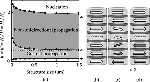
FIGURE 12.7 (a) Effect of dipolar interactions as a function of structure size on the phase diagram of a soliton stack with hu = 1. The dotted lines and arrows indicate where the boundary lies in the absence of dipolar interactions. (b–d): schematic of (b) a bulk antiparallel domain, (c) a chiral soliton, and (d) a sharp soliton.
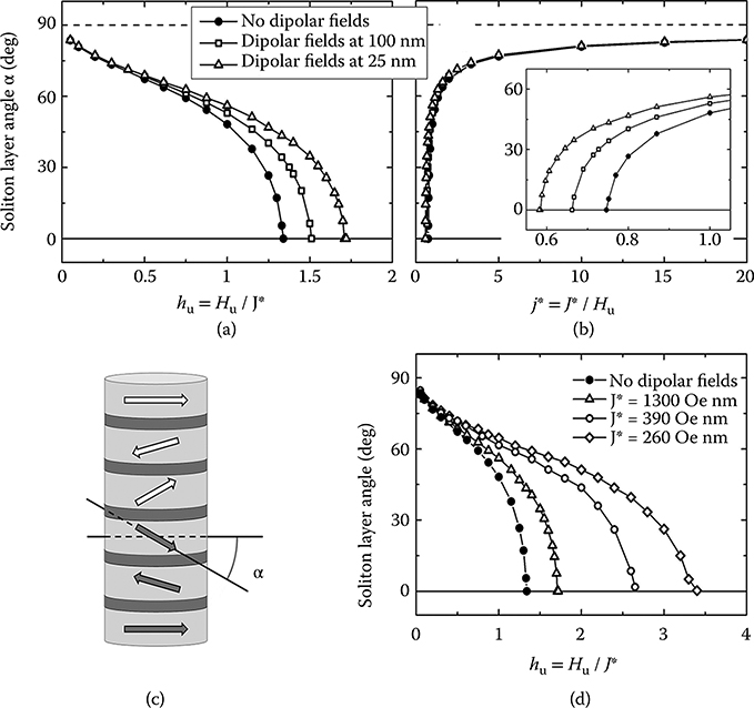
FIGURE 12.8 Effect of dipolar interactions on the soliton layer angle α. α as a function of (a) hu and (b) j*, without dipolar interactions (full circles), and in the presence of dipolar interactions at a lateral width of 100 nm (open squares) and 25 nm (open triangles). J* = 1300 Oe·nm. (c) Schematic illustrating how α is defined. (d) α as a function of hu without dipolar interactions (full circles) and with dipolar interactions at 25 nm lateral width, for J* = 1300 Oe·nm (open triangles), J* = 390 Oe·nm (open circles), and J* = 260 Oe·nm (open diamonds).
This is enough to explain the trends of the two remaining boundaries (triangles and squares) in Figure 12.7a: the way the corresponding switching fields change with structure size in Figure 12.7a is exactly reflected in the way the same boundaries vary with j* in the vicinity of j* = 1 in Figure 12.4b. In other words, increasing dipolar interactions has the same effect as increasing the effective AF coupling. More intuitively, the boundary between Correct propagation and Non-unidirectional propagation in Figure 12.7a (triangles) highlights the field at which the soliton goes from being chiral (Figure 12.7c) to being achiral (Figure 12.7d). As the width of the device decreases, and therefore as the splay between soliton layers increases, the chiral to achiral transition occurs at higher fields, in agreement with the observed increase of the field at which propagation becomes non-unidirectional as the width of the device decreases (triangles). The boundary between no propagation and correct propagation in Figure 12.7a (squares) indicates the field that is sufficient to overcome the energy barrier to forward propagation. This energy barrier decreases as j* increases (see Figure 12.5c).
We started this section by pointing to the fact that the simple hu or j* dependency of the ML’s behavior was lost in the presence of dipolar interactions. We just illustrated how the ML’s geometrical parameters (width and thicknesses) become relevant in the calculation of the phase diagram and the soliton angle for instance. Figure 12.8d illustrates some of the complexity inherent to dipolar interactions, particularly the fact that in their presence the absolute value of J* now matters. Figure 12.8d shows the soliton layer angle α as a function of hu in the absence of dipolar interactions (full circles) and with dipolar interactions at 25 nm width (open symbols), for J* = 1300 Oe·nm (triangles), 390 Oe·nm (circles), and 260 Oe·nm (diamonds). The latter three sets of data were calculated using the corresponding Hu (so that the explored range of hu remains the same). This might not correspond to any realistic material parameter, however, it illustrates how the simple scaling in the absence of dipolar fields, where α only depends on hu, is now lost. As can be seen on this figure, the effect of dipolar interactions at a fixed structure size is weaker for higher J*. This can be understood by the fact that dipolar interactions for a given width introduce an absolute field scale into the system, against which the nearest neighbor exchange coupling J* dominates or not. This will not be developed here, but by the same token, the width dependency of the hu = 1 phase boundary shown Figure 12.7a also depends on the absolute value of J* and Hu.
In conclusion, dipolar interactions present in any usefully small device do modify the functioning of the soliton shift register. Dipolar interactions create a long range AF coupling between layers that has the same qualitative effect as a higher effective nearest neighbor AF coupling. However, they introduce an absolute field scale, so that the simple scaling of the shift register’s properties with the ratio between nearest neighbor AF coupling field J* and anisotropy field Hu, j*, or hu, does not hold anymore. For the same structure size and for the same hu, the effect of dipolar interactions is stronger for lower J*. Nevertheless, for the parameters explicitly studied here (Fe on Cr [211]), the margin for correct soliton propagation is actually larger in the presence of dipolar interactions.
12.6.2 Full Micromagnetic Calculations
After dipolar interaction, the next obvious simplification of our calculations is the fact that we assume a macrospin model for the magnetization. However, how much of the behavior that we have just described would change if the full micromagnetic configuration was considered is unknown. Even the possibility of individual magnetic layers breaking into a multidomain state cannot be ruled out. There is no energetic gain for the bulk of the AP domain to break into vertically coupled AP domains, nonetheless, the layers at the center of a soliton could potentially break into domains during reversal. Even if the layers do not break into domains, the possible distortions of the magnetization allowed in full micromagnetics are likely to change their reversal behavior. There is no straightforward answer as to whether or not the soliton scheme would still work in full micromagnetics. As we have seen in Section 12.6.1, assuming specific geometrical parameters for our ML leads to setting a specific energy scale via the dipolar interactions. Furthermore, how close the dimensions of the device are from the single domain state will obviously make a difference: the smaller the device is, the better the macrospin approximation is. Because of the increased computation time, we have performed full micromagnetic simulations using the OOMMF software46 on a ML comprising a restricted number of layers, and for a small subset of parameters for which we have run the corresponding macrospin calculations. The micromagnetic simulation parameters are the following: anisotropy energy density Ku = 9.1 × 10⁴ J/m3, MS = 1400 emu/cm3, AF coupling energy density KAF = 1.36 × 10⁻⁴ J/m2, corresponding to the previously used parameters for Fe on Cr (211), and damping constant α = 0.5. The ML stack was made of eight layers, with tM = tS = 1.5 nm and a square lateral footprint of width = 200 nm. The cell size was 5 × 5 × 1.5 nm3.
It has to be noted that, because of edge effects, the behavior of a ML with such a reduced number of layers is likely to differ from the virtually infinite stack we have used for the macrospin simulations. However, the aim of this section is not to describe these differences. Rather, the aim of this section is to assess the limits of the macrospin model by directly comparing its predictions on a system with a reduced number of layers, which is tractable using full micromagnetic calculations.
The simulations were initialized with a left-handed soliton pointing toward +x straddling layers L3 and L4 by imposing an initial angle of ±45° on the soliton layers. An in-plane magnetic field of various amplitude and initially pointing in the +x direction was applied and subsequently rotated clockwise in steps of 5° for two complete cycles, leading, if the field amplitude is correct, to the propagation of the soliton in the upward direction. Different behaviors are observed, depending on the amplitude of the rotating field, which will not be detailed here. For a restricted range of applied fields, between 245 ± 5 Oe and 1175 ± 5 Oe, the soliton propagates one layer up the stack during the first half of the field cycle, from straddling L3–L4 to straddling L4–L5, then one more layer up during the second half of the first field cycle, from straddling L4–L5 to straddling L5–L6, finally another layer up to straddle L6–L7 during the first half of the second field cycle, immediately followed by the flipping of layers L7 and L8 and hence the annihilation of the soliton at the top of the stack. Figure 12.9b through 12.9f shows a few snapshots of the calculated magnetization configuration as the left-handed soliton propagates during the second half of the first field cycle. The top panel shows an xz-view of the ML, the bottom panels show an xy-view of layers L4, L5, and L6. Note the different scales in the xy-plane and along the z axis. The middle panel shows the direction of the applied rotating magnetic field. When the field points toward −x (Figure 12.9b), the soliton has already propagated one layer up during the first half of the first cycle (it straddles layers L4 and L5) and the soliton layers point toward −x. As the field rotates further (Figure 12.9c), the magnetization in the top layer of the soliton (L5) rotates, until somewhere between 280° (Figure 12.9d) and 285° (Figure 12.9e), the x-component of the magnetization in layer L5 changes sign and the soliton propagates one layer up to straddle layers L5 and L6.
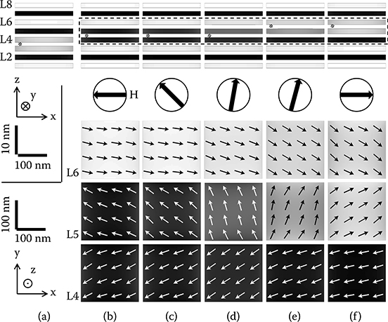
FIGURE 12.9 (a) Initial magnetic state for the micromagnetic simulations. The contrast ranges from black (−x) to white (+x). A soliton pointing in the +x direction straddles layers L3 and L4. (b–f): Snapshots of the micromagnetic configuration for an eight layers multilayer where a soliton propagates from between L4 and L5 to between L5 and L6 under an applied rotating field of 500 Oe. The soliton is marked by an asterisk. Top panels: (z, x)-view; bottom panels: (x, y)-view. Note the different scale bars in the z direction and in the (x, y)-plane shown in the bottom panels of (a). The black arrow inside the circle indicates the field direction. As measured from the +x axis: (b) 180°; (c) 225°; (d) 280°; (e) 285°; (f) 0°.
Figure 12.10a shows a polar plot of the field amplitude/angle at which the previously described transition occurs (controlled propagation of the left-handed soliton from straddling L4 and L5 to straddling L5 and L6, see Figure 12.10b). For both macrospin and micromagnetic simulations, the transition point is determined as the angle for which, under a given field, the average magnetization in the layer changes sign. For H = 500 Oe, we have checked that this transition indeed corresponds to soliton propagation, that is, that if the applied field is turned off from the configuration shown in Figure 12.9d, the soliton stays in between layers L4 and L5, whereas if the applied field is turned off from the configuration shown in Figure 12.9e, the soliton stays in between layers L5 and L6.
Micromagnetic simulations are shown in gray; the corresponding macrospin simulations are shown in black. Two different behaviors are observed in the macro-spin calculations. For low fields (open black squares, below 675 ± 5 Oe), the same controlled propagation of the soliton up the stack is seen. For field amplitudes above 675 Oe (full black circles), the macrospin model shows that the soliton ceases to propagate unidirectionally, in close quantitative agreement with the results of Figure 12.7 at 200 nm width, despite the fact that the number of layers was a lot larger. In contrast, the micromagnetic simulations show correct unidirectional propagation for fields up to 1175 Oe. Loss of unidirectionality with increasing field was attributed to a loss of chirality as the field becomes high enough so that both soliton layers point exactly in the direction of the field. However, when looking into details at the micromagnetic configuration of the soliton layers, it is clear that, although the splay between soliton layers is greatly reduced as the applied field increases, the memory of the chirality is not totally erased as it is in the macrospin model (see Figure 12.10c through e). At high fields, the soliton layers are in an S-state, where most of the magnetization points along the field direction, apart from the two edges perpendicular to the field, which point closer to the direction set by the initial soliton chirality.
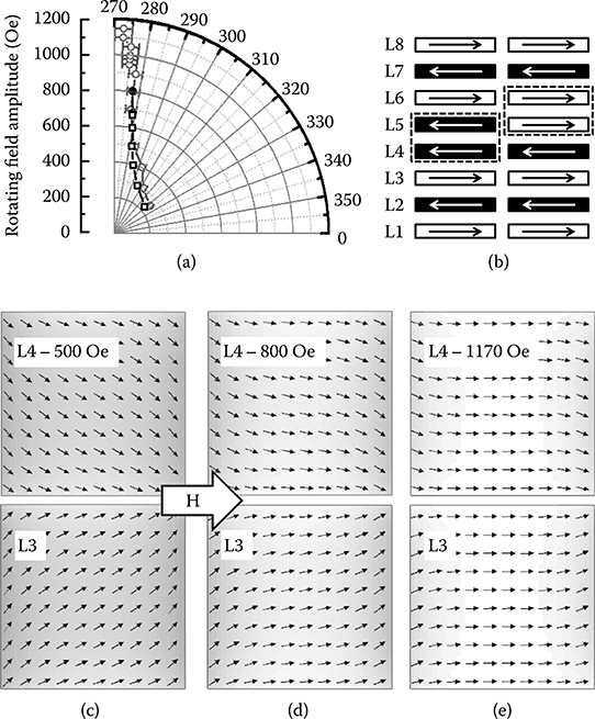
FIGURE 12.10 (a) Polar plot showing the applied field amplitude and angle at which L5 switches as a soliton propagates from between L4 and L5 to between L5 and L6. The angle is measured clockwise from the + x axis. (b) Schematic of the transition considered. (c, d, e) Micromagnetic configurations of layers L3 and L4 when carrying a soliton under various field amplitudes. The field is applied in the +x direction, as indicated by the large white arrow.
For field amplitudes higher than 1175 Oe, however, on initializing the soliton between L3 and L4, the soliton moves backwards down to in between L2 and L3 before annihilating at the bottom of the ML. In this case also, the field is actually not strong enough to completely erase the chiral identity of the soliton, which is still imprinted in the direction of the magnetization in the soliton layers along the edge of the structure, as in Figure 12.10e. This is beyond the scope of this paper, but we have observed that in a homogeneous ML such as the one studied here, the edge of a ML acts as a well for solitons. In our case here, this attraction is strong enough and the chiral identity of the soliton is weak enough that we observe a flipping of the chirality of the soliton, followed by its downward motion.
In brief, the qualitative agreement between macrospin and micromagnetic simulations for these particular material parameters and at 200 nm lateral width is excellent. Both show that controlled propagation of the soliton occurs at a field angle closer and closer to the hard axis for increasing field amplitudes. Quantitatively, the agreement is very good at low fields. At high field, the macrospin model underestimates the field at which the soliton will lose its chirality and unidirectional propagation will be lost, so that the calculated operating margin is larger in micromagnetics that in macrospin. Again, this constitutes in no way a general rule, and different material parameters might behave differently.
12.7 Conclusion
In conclusion, we have presented the results of macrospin simulations that show the existence of mobile chiral topological kink solitons in AF-coupled MLs with in-plane uniaxial anisotropy. We have demonstrated that in the absence of dipolar interactions, the behavior of these systems is solely described by the anisotropy to coupling ratio hu. We showed that they can couple to an external in-plane rotating magnetic field and propagate synchronously in the vertical direction. As opposed to our previously demonstrated soliton-carrying ML scheme with perpendicular anisotropy,34 the propagation of in-plane solitons such as the ones studied here is bidirectional and depends on the relative chirality of the soliton and the rotating field. We showed that several solitons can propagate controllably in the same ML stack and we described the soliton–soliton interaction mechanism. We have studied how including dipolar interactions into the macrospin calculations modifies the behavior of a ML. We showed that the main consequence of including dipolar interactions is to lose the simple dependency of the behavior of soliton-carrying stacks on hu. Indeed, dipolar interactions depend on the geometrical parameters of the ML (lateral size and thicknesses) and therefore their inclusion adds several independent degrees of freedom. The effect of dipolar interactions is qualitatively similar to an increase in the nearest neighbor AF coupling. However, the fact that dipolar interactions are long-range means this is only a coarse approximation. We have also shown that the strength of the modifications caused by dipolar interactions depends on the absolute strength of the AF coupling J*. Dipolar interactions calculated for a given set of geometrical parameters have a stronger effect for a small J* than for a large J*. We have also studied the limits of the macrospin approximation by performing full micro-magnetic simulations for a particular set of parameters and a small number of layers. We showed that for this particular set of material parameters and dimensions, the qualitative agreement between the macrospin model and micromagnetics was excellent. Discrepancies were found quantitatively, in that case showing that the range of field for which the soliton propagates correctly is larger in the case of micromagnetic simulations than in the macrospin case.
Because of their properties as stable, mobile objects formed in synthetic magnetic systems, solitons in magnetic MLs are ideal candidates to code and manipulate digital information in a three-dimensional spintronic device.47
Acknowledgments
This work was supported by the European Community under the Seventh Framework Program ERC contract no. 247368 (3SPIN) and grant agreement no. 309589 (M3D). A. Fernández-Pacheco acknowledges support by a Marie Curie IEF within the Seventh European Community Framework Program no. 251698 (3DMAGNANOW). R. Lavrijsen is gratefully acknowledged for his critical reading of parts of this manuscript.
References
1. S. A. Wolf, D. D. Awschalom, R. A. Buhrman, J. M. Daughton, S. von Molnár, M. L. Roukes, A. Y. Chtchelkanova, and D. M. Treger, Spintronics: A Spin-Based Electronics Vision for the Future, Science 294, 1488 (2001).
2. R. P. Cowburn and M. E. Welland, Room Temperature Magnetic Quantum Cellular Automata, Science 287, 1466 (2000).
3. D. A. Allwood, G. Xiong, C. C. Faulkner, D. Atkinson, D. Petit, and R. P. Cowburn, Magnetic Domain-Wall Logic, Science 309, 1688 (2005).
4. A. Imre, G. Csaba, L. Ji, A. Orlov, G. H. Bernstein, and W. Porod, Majority Logic Gate for Magnetic Quantum-Dot Cellular Automata, Science 311, 205 (2006).
5. S. I. Kiselev, J. C. Sankey, I. N. Krivorotov, N. C. Emley, R. J. Schoelkopf, R. A. Buhrman, and D. C. Ralph, Microwave oscillations of a nanomagnet driven by a spin-polarized current, Nature 425, 380 (2003).
6. V. Baltz, B. Rodmacq, A. Bollero, J. Ferré, S. Landis, and B. Dieny, Balancing interlayer dipolar interactions in multilevel patterned media with out-of-plane magnetic anisotropy, Appl. Phys. Lett. 94, 052503 (2009).
7. I. Tudosa, J. A. Katine, S. Mangin, and E. E. Fullerton, Perpendicular spin-torque switching with a synthetic antiferromagnetic reference layer, Appl. Phys. Lett. 96, 212504 (2010).
8. S. S. P. Parkin, N. More, and K. P. Roche, Oscillations in exchange coupling and magnetoresistance in metallic superlattice structures: Co/Ru, Co/Cr, and Fe/Cr, Phys. Rev. Lett. 64, 2304 (1990).
9. S. W. Cheong and M. Mostovoy, Multiferroics: a magnetic twist for ferroelectricity, Nature Mater. 6, 13 (2007).
10. Y. Togawa, T. Koyama, K. Takayanagi, S. Mori, Y. Kousaka, J. Akimitsu, S. Nishihara, K. Inoue, A. S. Ovchinnikov, and J. Kishine, Chiral Magnetic Soliton Lattice on a Chiral Helimagnet, Phys. Rev. Lett. 108, 107202 (2012).
11. A. N. Bogdanov and D. A. Yablonskiǐ, Thermodynamically stable “vortices” in magnetically ordered crystals. The mixed state of magnets, Sov. Phys. JETP 68, 101 (1989).
12. U. K. Rosler, A. N. Bogdanov, and C. Pfleiderer, Spontaneous skyrmion ground states in magnetic metals, Nature 442, 797 (2006).
13. S. Mühlbauer, B. Binz, F. Jonietz, C. Pfleiderer, A. Rosch, A. Neubauer, R. Georgii, and P. Böni, Skyrmion Lattice in a Chiral Magnet, Science 323, 915 (2009).
14. X. Z. Yu, Y. Onose, N. Kanazawa, J. H. Park, J. H. Han, Y. Matsui, N. Nagaosa, and Y. Tokura, Real-space observation of a two-dimensional skyrmion crystal, Nature 465, 901 (2010).
15. S. Heinze, K. von Bergmann, M. Menze, J. Brede, A. Kubetzka, R. Wiesendanger, G. Bihlmayer, and S. Blügel, Spontaneous atomic-scale magnetic skyrmion lattice in two dimensions, Nature Physics 7, 713 (2011).
16. I. Raicević, D. Popović, C. Panagopoulos, L. Benfatto, M. B. Silva Neto, E. S. Choi, and T. Sasagawa, Skyrmions in a Doped Antiferromagnet, Phys. Rev. Lett. 106, 227206 (2011).
17. I. Dzyaloshinskii, A thermodynamic theory of “weak” ferromagnetism of antiferromagnetics, J. Phys. Chem. Solids 4, 241 (1958).
18. T. Moriya, Anisotropic Superexchange Interaction and Weak Ferromagnetism, Phys. Rev. 120, 91 (1960).
19. A. P. Malozemoff and J. C. Slonczewski, Magnetic Domain Walls in Bubble Materials, Academic Press, New York, NY (1979).
20. C. Moutafis, S. Komineas, C. A. F. Vaz, J. A. C. Bland, T. Shima, T. Seki, and K. Takanashi, Magnetic bubbles in FePt nanodots with perpendicular anisotropy, Phys. Rev. B 76, 104426 (2007).
21. A. Yoshimori, A New Type of Antiferromagnetic Structure in the Rutile Type Crystal, J. Phys. Soc. Jpn. 14, 807 (1959).
22. K. Marty, V. Simonet, E. Ressouche, R. Ballou, P. Lejay, and P. Bordet, Single Domain Magnetic Helicity and Triangular Chirality in Structurally Enantiopure Ba3NbFe3Si2O14, Phys. Rev. Lett. 101, 247201 (2008).
23. Y. Hiraoka, Y. Tanaka, T. Kojima, Y. Takata, M. Oura, Y. Senba, H. Ohashi, Y. Wakabayashi, S. Shin, and T. Kimura, Spin-chiral domains in Ba0.5Sr1.5Zn2Fe12O22 observed by scanning resonant x-ray microdiffraction, Phys. Rev B 84, 064418 (2011).
24. D. L. Mills, Surface Spin-Flop State in a Simple Antiferromagnet, Phys. Rev. Lett. 20, 18 (1968).
25. D. L. Mills and W. M. Saslow, Surface Effects in the Heisenberg Antiferromagnet, Phys. Rev. 171, 488 (1968).
26. A. S. Carrico, R. E. Camley, and R. L. Stamps, Phase diagram of thin antiferromagnetic films in strong magnetic fields, Phys. Rev. B 50, 13453 (1994).
27. N. Papanicolaou, The ferromagnetic moment of an antiferromagnetic domain wall, J. Phys.: Condens. Matter 10, L131 (1998).
28. R. W. Wang, D. L. Mills, E. E. Fullerton, J. E. Mattson, and S. D. Bader, Surface spin-flop transition in Fe/Cr(211) superlattices: Experiment and theory, Phys. Rev. Lett 72, 920 (1994).
29. S. Rakhmanova, D. L. Mills, and E. E. Fullerton, Low-frequency dynamic response and hysteresis in magnetic superlattices, Phys. Rev. B 57, 476 (1998).
30. S. G. E. te Velthuis, J. S. Jiang, S. D. Bader, and G. P. Felcher, Spin Flop Transition in a Finite Antiferromagnetic Superlattice: Evolution of the Magnetic Structure, Phys. Rev. Lett. 89, 127203 (2002).
31. J. Meersschaut, C. Labbé, F. M. Almeida, J. S. Jiang, J. Pearson, U. Welp, M. Gierlings, H. Maletta, and S. D. Bader, Hard-axis magnetization behavior and the surface spin-flop transition in antiferromagnetic Fe/Cr(100) superlattices, Phys. Rev. B 73, 144428 (2006).
32. A. Fernández-Pacheco, D. Petit, R. Mansell, R. Lavrijsen, J. H. Lee, and R. P. Cowburn, Controllable nucleation and propagation of topological magnetic solitons in CoFeB/Ru ferrimagnetic superlattices, Phys. Rev. B 86, 104422 (2012).
33. V. G. Baryakhtar, M. V. Chetkin, B. A. Ivanov, and S. N. Gadetskii, Dynamics of Topological Magnetic Solitons: Experiment and Theory, Springer-Verlag, Berlin, Germany (1994).
34. R. Lavrijsen, J. H. Lee, A. Fernndez-Pacheco, D. Petit, R. Mansell, and R. P. Cowburn, Magnetic ratchet for three-dimensional spintronic memory and logic, Nature 493, 647 (2013).
35. S. Chikazumi, Physics of Magnetism, John Wiley & Sons, New York, NY (1964).
36. D. A. Allwood, N. Vernier, Gang Xiong, M. D. Cooke, D. Atkinson, C. C. Faulkner, and R. P. Cowburn, Shifted hysteresis loops from magnetic nanowires, Appl. Phys. Lett. 81, 4005 (2002).
37. E. E. Fullerton, M. J. Conover, J. E. Mattson, C. H. Sowers, and S. D. Bader, Oscillatory interlayer coupling and giant magnetoresistance in epitaxial Fe/Cr(211) and (100) superlattices, Phys. Rev. B 48, 15755 (1993).
38. A. T. Hindmarch, A. W. Rushforth, R. P. Campion, C. H. Marrows, and B. L. Gallagher, Origin of in-plane uniaxial magnetic anisotropy in CoFeB amorphous ferromagnetic thin films, Phys. Rev. B 83, 212404 (2011).
39. H. Raanaei, H. Nguyen, G. Andersson, H. Lidbaum, P. Korelis, K. Leifer, and B. Hjörvarsson, Imprinting layer specific magnetic anisotropies in amorphous multilayers, J. Appl. Phys. 106, 023918 (2009).
40. T. J. Klemmer, K. A. Ellis, L. H. Chen, B. van Dover, and S. Jin, Ultrahigh frequency permeability of sputtered Fe–Co–B thin films, J. Appl. Phys. 87, 830 (2000).
41. W. Yu, J. A. Bain, W. C. Uhlig, and J. Unguris, The effect of stress-induced anisotropy in patterned FeCo thin-film structures, J. Appl. Phys. 99, 08B706 (2006).
42. R. P. Cowburn, Property variation with shape in magnetic nanoelements, J. Phys. D: Appl. Phys. 33 R1 (2000).
43. S. S. P. Parkin, Oscillations in giant magnetoresistance and antiferromagnetic coupling in [Ni81Fe19/Cu]N multilayers, Appl. Phys. Lett. 60, 512 (1992).
44. I. G. Trindade, Antiferromagnetically coupled multilayers of (Co90Fe10 tF/Ru tRu) × N and (Ni81Fe19 tF/Ru tRu) × N prepared by ion beam deposition, J. Magn. Magn. Mat. 240, 232 (2002).
45. G. Akoun and J. P. Yonnet, 3D analytical calculation of the forces exerted between two cuboidal magnets, IEEE Trans. Mag. 20, 1962 (1984).
46. OOMMF, M.J. Donahue, and D.G. Porter, Interagency Report NISTIR 6376, National Institute of Standards and Technology, Gaithersburg, MD (Sept. 1999), http://math.nist.gov/oommf.
47. Patent numbers GB0820844.9, Cowburn, Russell Paul. Magnetic data storage, U.S. Patent 20100128510, filed November 13, 2009, and issued May 27, 2010.