
15 Memristor-CMOS-Hybrid Synaptic Devices Exhibiting Spike-Timing-Dependent Plasticity
Tetsuya Asai
Contents
15.2 CMOS-ReRAM-Hybrid Synaptic Circuit
15.3 Experimental and Simulation Results
15.3.1 Evaluation of Memristors
15.3.2 Experimental Results of ReRAM-CMOS-Hybrid Synaptic Devices
15.1 Introduction
One of a challenging issue in developing brain-inspired hardware is to implement nonvolatile analog synaptic devices in a compact structure. Various types of volatile (capacitor-based) analog synaptic devices have been developed [1–3], whereas types of nonvolatile analog synaptic devices are limited so far. Present nonvolatile synaptic devices use flash-based or its alternative technologies [4–6], however, they had difficulties in designing compact circuits for electron injection and ejection as well as in establishing the high reliability.
Recently, the so-called “memristor” originally introduced by Leon Chua in 1971 [7], which was claimed to be the fourth circuit element exhibiting the relationship between flux φ and charge q, has been respotlighted since Strukov et al. [8] presented the equivalent physical examples. The presented device was a bipolar ReRAM, and did not directly exhibit the relationship [φ = f(q)], however, the device could demonstrate its equivalent dynamics given by the temporal deviation of φ = f(q) as
where M(q) represents the memristance, v the voltage across the memristor, and i the current of the memristor.
Memristive devices could naturally be exploited for implementing nonvolatile synapses on electronic circuits because they are equivalent to resistors whose resistances can be held or modulated by the amount of the integrated current. Using possible memristive nanojunctions, a digital-controlled neural network has been introduced by Snider [9], and the concept has been expanded to use a nanowire-crossbar add-on as well as memristive (two-terminal) crosspoint devices such as nanowire resistive RAMs [10]. This chapter introduces yet-another analog approach, that is, a memristor (ReRAM)-based analog synaptic circuit, for possible neuromorphic computers having complementary metal-oxide-semiconductor (CMOS)-ReRAM-hybrid structures.
15.2 CMOS-ReRAM-Hybrid Synaptic Circuit
Key ideas to implement novel synaptic circuits in this chapter are (1) to regard a memristor as a synaptic junction, and (2) to assign a membrane capacitor in one terminal of a memristor, as shown in Figure 15.1. An input node of the memristor accepts presynaptic voltage spikes (Vpre), and the other node is connected to membrane capacitor Cpre. Because this capacitor is charged or discharged by the input spike via the memristor having variable resistance (Rmem), a postsynaptic potential (VPSP) is generated on the node where the time constant is given by Cpre Rmem.
At the rising edge of Vpre (spike onset), Cpre is charged via the memristor, and because of the charge flow (current) the memristor’s conductance is increased, in case of the polarity settings shown in Figure 15.1. Then at the falling edge of Vpre, Cpre is discharged, and the memristor’s conductance is decreased. Here it should be noticed that the absolute amount of the charge passing the memristor during the charging operation is equal to that of the discharging operation, which indicates that the memristor’s conductance before applying a spike should be equal to the subsequent conductance after applying the spike, which I call “conductance-preservation law” in ideal C-memristor circuits.
Figure 15.2 shows a setup for modulating the memristor’s conductance, as well as a postsynaptic-current (IPSC) readout circuitry. Because a MOSFET has nonlinear characteristics between the gate voltage and the drain current, by integrating the drain currents of M0 on the other (neuronal membrane) capacitor, one obtains different membrane potentials for different conductance of the memristor.
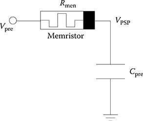
FIGURE 15.1 Fundamental unit of memristor STDP circuit.
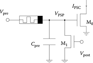
FIGURE 15.2 Conductance modulation and readout circuitry in C-memristor circuit.
If the membrane potential exceeds a given threshold voltage, a postneuron circuit (standard integrate-and-fire circuit) generates a voltage spike (Vpost in Figure 15.2). At the same time, the PSP node is shunted by an additional MOSFET (M1). Therefore, because of the potential difference across the memristor, the conductance is increased, which exhibits STDP in the memristor synapse (for the timing difference Δt > 0), that is, the timing difference between pre- and postsynaptic spikes results in the differential synaptic weights (differential conductance of the memristor).
15.3 Experimental and Simulation Results
Figure 15.3 shows an array of memristors (bipolar ReRAMs) with NiO thin films (Pt–NiO–Pt), which was fabricated by the author’s collaborators in Osaka University, Japan. It consists of 9 × 9 memristor equivalents and has a common indium electrode that is connected to all the memristors. The following experimental results were obtained by using this ReRAM device.
15.3.1 Evaluation of Memristors
As described in Section 15.1, an original model of memristors is represented in terms of memristance, M(q); however, here let us compare memristor models and physical ReRAMs by using a comprehensive model shown by D.B. Strukov et al. [8]:
where i represents the current of a memristor, v the voltage across a memristor, w the state variable of a memristor that corresponds to the amount of transported charges across the memristor, and g(w) the monotonic increasing function representing variable conductance for w. Obviously this model explains that g(w) is increased (or decreased) by positive (or negative) i. Therefore, if a constant current is given to a memristor, as shown in an inset of Figure 15.4, the conductance of memristor will increase and hence, the voltage across the memristor will decrease, as long as the model is qualitatively equivalent to physical bipolar ReRAMs. Figure 15.4 plots the transient voltage across the memristor when a constant current of 10 nA was given to the memristor. This result showed that the voltage decreases as time increases, and hence, the model is qualitatively equivalent to the bipolar ReRAM.
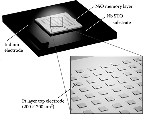
FIGURE 15.3 Array of bipolar ReRAM (memristor equivalent) (9 × 9 memristors on common substrate).
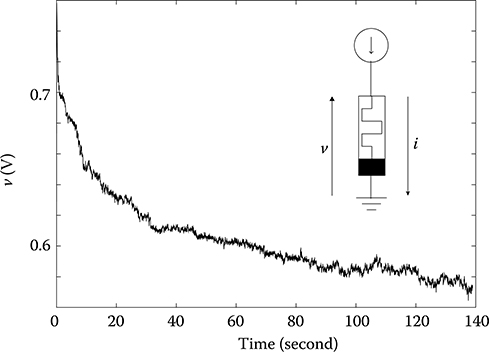
FIGURE 15.4 Experimental results of primitive memristor.
A voltage bias has to be given across ReRAMs to measure their current-voltage (IV) characteristics (differential conductance of ReRAMs); however, every voltage sweep may change the conductance due to the current flow caused by the sweeping operation. Therefore, one has to decrease the voltage to avoid the unwanted change of the conductance through measurements, whereas if the voltage is too small, the current measurement becomes difficult because of thermal and environmental noises. Hence, one has to estimate moderate ranges of voltage sweeps before starting evaluations. Figure 15.5a and b plots IV characteristics of the 1st and 20th sweeps (sweep time: 640 μs) with sweeping range of 0.2 V and 1.4 V, respectively. When the range was set at 0.2 V (Figure 15.5a), no significant change of the differential conductance between the 1st and 20th measurements was observed, whereas the differential conductance of the 1st and 20th measurements was significantly changed when the range was set at 1.4 V (Figure 15.5b). Moreover, when the range was smaller than 50 mV, the IV characteristics became noisy. On the basis of these experiments, in the following experiments, the sweep range was set at 0.2 V for measuring differential conductance.
Figure 15.6 exhibits dependence of increase or decrease of differential conductance on the ReRAM’s polarity. The initial IV curve is represented by (a) in the figure. Then a single current pulse (amplitude: 10 μA; pulse width: 640 μs [microseconds]) was given to the ReRAM where the current direction is indicated by an arrow of IReRAM. The resulting IV curve is represented by (b) where the differential conductance was increased by the single current pulse. Then the same current pulse was applied to the ReRAM in opposite direction (of an arrow of IReRAM.), and the resulting IV curve is represented by (c) where the differential conductance was decreased by the pulse. The results clearly show the dependence of increase or decrease of differential conductance on the ReRAM’s polarity. It should be noticed that there exists small difference between curves (a) and (c) although the same current pulses were applied in different directions. This might be due to asymmetrical structure of the ReRAMs, and in case of symmetrical ReRAMs, for example, nanowire crossbars of memristive materials, the curves will be the same.
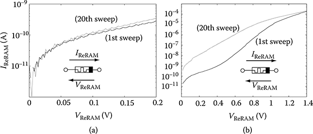
FIGURE 15.5 Experiments to determine voltage sweep ranges. (a) 0–0.2 V sweep and (b) 0–1.4 V sweep results.
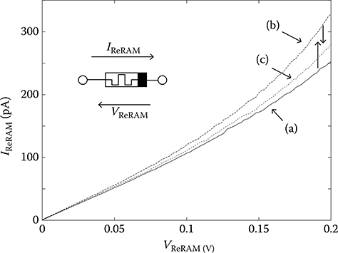
FIGURE 15.6 Dependence of increase or decrease of differential conductance on ReRAM’s polarity.
In practical ReRAMs, when large voltage or current is forwardly (or reversely) applied, the conductance will be fixed to large (or small) values. This is typical behavior of ReRAM to be operated as binary memory devices; however, this property is not suitable for their analog applications. In fact, experiments shown in Figure 15.6 were performed by setting the initial differential conductance to its minimum, to avoid the conductance saturation to its maximum. Therefore, one has to estimate appropriate amplitudes and widths of current pulses that do not make ReRAM’s conductance saturated. To estimate the amplitudes and widths, differential conductance were measured by repeating the same experiments as in Figure 15.6.
Figure 15.7 shows the results. In Figure 15.7a, five current pulses were given to the ReRAM (current direction is indicated by an arrow of IReRAM), whereas three pulses in opposite directions were applied to the ReRAM in Figure 15.7b. As the conductance were not saturated within these range of pulses, as long as one uses the current pulse (amplitude: 10 μA; pulse width: 640 μs), the single pulse will not make the ReRAM’s conductance saturated.
Figure 15.8 represents IV plots of sequential modifications (increase and decrease) of differential conductance by applying unidirectional current pulses. The minimum conductance is represented by (a), whereas (b) represents the intermediate (nonsaturated) conductance. This result clearly shows that the conductance can be modified from the intermediate (nonsaturated) state of ReRAMs.
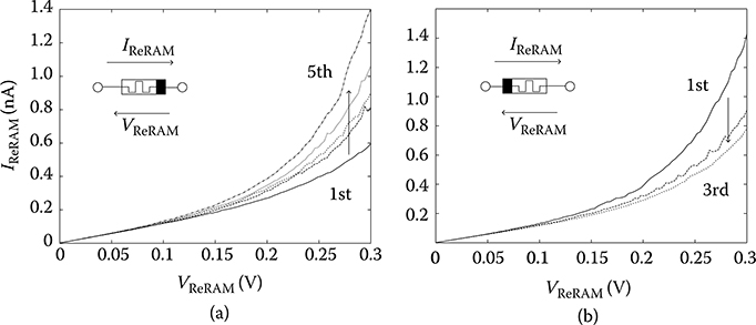
FIGURE 15.7 Dependence of differential conductance on ReRAM’s polarity. (a) Forward sweep. (b) Backward sweep.
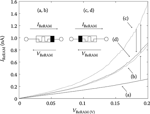
FIGURE 15.8 IV plots of sequential modifications (increase and decrease) of differential conductance.
15.3.2 Experimental Results of ReRAM-CMOS-Hybrid Synaptic Devices
Through experiments in Section 15.3.1, now we are ready to start the experiments of ReRAM-CMOS-hybrid synaptic devices. First, the ReRAM-C circuit (shown in Figure 15.1) was assembled inside a shield box of semiconductor parameter analyzer with a discrete capacitor (C = 0.5 nF). The result is shown in Figure 15.9. In this experiment, voltage pulse Vpre was applied to the circuit, and VPSP and current of the capacitor (current flowing into the ground) were measured. Then the IV curve was calculated by the data because one cannot measure IV characteristics when the pulse is raised. In Figure 15.9, (a) represents the IV curve before the raise of Vpre, whereas (b) represents the IV curve after the fall of Vpre, which shows there is no significant difference between the pre- and postdifferential conductance.
Figure 15.10 shows experimental results of ReRAM-C-nMOS circuit shown in Figure 15.2 where discrete nMOSFET 2SK1398 was used and readout nMOS M0 was omitted in this experiment. In Figure 15.10a, Vpost was always set at 0 and a voltage pulse was applied to Vpre only. During the experiments, VPSP and Cpre’s current were measured, and the IV characteristics of the memristors were reconstructed before/during/after applying the voltage spike. In the figure, plots indicated by (i) represent the initial IV characteristics of the memristor (before applying the spike), (ii) the intermediate IV characteristics (after the spike onset), and (iii) the subsequent characteristics (after the falling edge of the spike). It should be noticed that although the conductance was increased during the intermediate state, the final conductance (iii) was almost equal to the initial conductance (i), even in real experiments. Figure 15.10b shows the opposite case, that is, the resulting conductance (iii) was increased as compared with initial conductance (i) by applying a spike as Vpost. In this experiment, Cpre was charged by Vpre and then was discharged by Vpost, which means that the absolute amount of the charge passing the memristor during the charging operation is not equal to that of the discharging operation. The result implied that the conductance could be modified by the difference of spike timings of pre- and postsynaptic neurons (Δt).
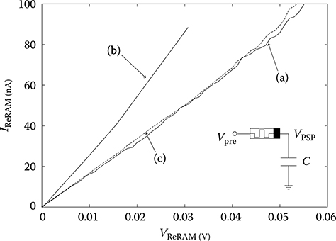
FIGURE 15.9 Experimental IV curves of memristor-C circuit. (a) Initial sweep, (b) reconstructed IV at spike onset, and (c) reconstructed IV at spike offset.
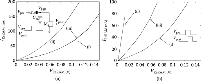
FIGURE 15.10 Experimental results of (a) conductance preservation and (b) modulation.
Figure 15.11 exhibits a part of STDP experiments with the synaptic device. In the experiment, two voltage spikes as illustrated in Figure 15.11a were used where the timing difference between pre- and postspike voltages (Vpre and Vpost) was defined as Δt. Figure 15.11b shows the results of conductance modulation for different timing values. When Δt was large, the differential conductance (Δg) before and after applying the spike, was small as expected, whereas when Δt was decreased to 0, Δg was exponentially increased. This result clearly showed that the conductance could be controlled by the spike-timing difference (Δt).
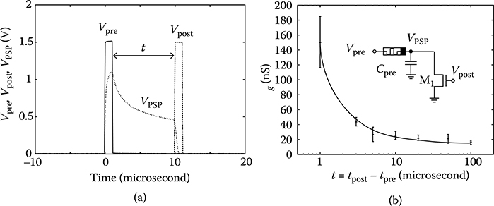
FIGURE 15.11 Experimental results of half STDP characteristics of memristor-CMOS hybrid circuit. (a) Definition of spike timing difference Δt between pre and post spikes (Vpre and Vpost). (b) Change of conductance Δg as function of spike timing difference Δt.
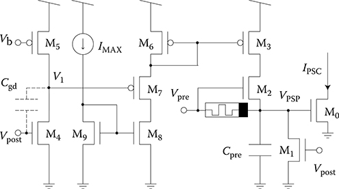
FIGURE 15.12 Proposed STDP synaptic circuit having asymmetric time window.
The circuit shown in Figure 15.2 does not modify memristor’s conductance when Δt < 0 because when Vpre = 0 (VPSP = 0), the memristor’s current is always zero even if M1 is turned on or off by Vpost. To obtain Δt < 0 responses, the circuit has been extended where additional MOSFETs (M2–M5) are employed, as shown in Figure 15.12. M4 and M5 act as a source-common amplifier and exhibit large time delay, which can be controlled by Vb, on voltage V1 upon the falling edge of Vpost because Cgd is amplified by the mirror effect. When M7 is turned on (just after the firing of Vpost), IMAX is mirrored to M3 via current mirrors M8–M9 and M3–M6. At the same time, if M2 is turned on by Vpre, VPSP is increased. Consequently, at the falling edge of Vpre, conductance of the memristor is decreased.
Figure 15.13 shows the simulation results indicating asymmetric STDP characteristics. In the simulations, IV characteristics of the fabricated memristor shown in Figure 15.3 (used in previous experiments) were assumed, and models of a discrete MOS device (2SK1398 and 2SJ184) and a capacitor (0.1 μF) were used. The result clearly showed that the differential conductance (ΔGMEM) was modified by the difference of spike timings of pre- and postsynaptic neurons (Δt).
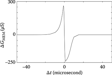
FIGURE 15.13 Simulated asymmetric STDP characteristics of proposed circuit shown in Figure 15.12.
15.4 Conclusion
A memristor-based STDP synaptic device was introduced. The device was built based on a combination of a capacitor and a memristor by controlling the so-called conductance-preservation law. First, a fundamental device consisting of memristor-equivalent devices called resistive RAMs as well as a discrete capacitor and a MOSFET was introduced and demonstrated by extensive experimental results. Then an STDP synaptic device was introduced where the device exhibited conductance preservation, modulation, the resulting STDP characteristics for positive timing difference between pre- and postsynaptic voltage spikes (Δt > 0). Finally, to mimic STDP characteristics in Δt < 0, the device was modified to the circuit level, by adding several MOSFETs. Through SPICE simulations, I showed that the circuit could exhibit asymmetric STDP characteristics.
Memristive devices (e.g., ReRAMs and atomic switches) offer a promising alternative for the implementation of nonvolatile analog synapses. They are applied in the CMOS molecular (CMOL) architecture [11], which combines memristive nanojunctions with CMOS neurons and their associated controllers. In ITRS 2007 [12], CMOL was introduced in terms of nanogrids of (ideally) single molecules fabricated on top of a traditional CMOS layer, but the concept has since been expanded to use a nanowire-crossbar add-on as well as memristive (two-terminal) crosspoint devices such as nanowire ReRAMs. The CMOL architecture will be further expanded to include multiple stacks of CMOS layers and crossbar layers. This may result in the implementation of large-scale multilayer neural networks, which have thus far evaded direct implementations by CMOS devices only.
Acknowledgments
The author thanks Dr. Keisuke Oka, Prof. Takeshi Yanagida, and Prof. Tomoji Kawai of Osaka University for their supplying memristor-equivalent devices (array of ReRAMs). This study was supported by a Grant-in-Aid for Scientific Research on Innovative Areas [20111004] from the Ministry of Education, Culture Sports, Science and Technology (MEXT) of Japan.
References
1. Y. Kanazawa, T. Asai, M. Ikebe, and Y. Amemiya, A novel CMOS circuit for depressing synapse and its application to contrast-invariant pattern classification and synchrony detection, International Journal of Robotics and Automation, 19(4): 206–212, 2004.
2. H. Tanakaa, T. Morie, and K. Aihara, A CMOS circuit for STDP with a symmetric time window, International Congress Series, 1301: 152–155, Elsevier, 2007.
3. H. Tanaka, T. Morie, and K. Aihara, A CMOS spiking neural network circuit with symmetric/asymmetric STDP function, IEICE Transactions on Fundamentals, E92-A(7): 1690–1698, 2009.
4. K. Nakajima, S. Sato, T. Kitaura, J. Murota, and Y. Sawada, Hardware implementation of new analog memory for neural networks, IEICE Transactions on Electronics, E78-C(1): 101–105, 1995.
5. C. Diorio, P. Hasler, B. Minch, and C. Mead, Floating-gate MOS synapse transistors, Neuromorphic Systems Engineering, The Kluwer International Series in Engineering and Computer Science, 447(4): 315–337, 1998.
6. S. Kinoshita, T. Morie, M. Nagata, and A. Iwata, A PWM analog memory programming circuit for floating-gate MOSFETs with 75-μs programming time and 11-bit updating resolution, IEEE Journal of Solid-State Circuits, 36(8): 1286–1290, 2001.
7. L.O. Chua, Memristor—the missing circuit element, IEEE Transactions on Circuit Theory, 18: 507–519, 1971.
8. D.B. Strukov, G.S. Snider, D.R. Stewart, and R.S. Williams, The missing memristor found, Nature, 453(1): 80–83, 2008.
9. G.S. Snider, Self-organized computation with unreliable, memristive nanodevices, Nanotechnology, 18(36): 365202, 2007.
10. S.H. Jo, T. Chang, I. Ebong, B.B. Bhadviya, P. Mazumder, W. Lu, Nanoscale memristor device as synapse in neuromorphic systems, Nano Letters, 10(4): 1297–1301, 2010.
11. K.K. Likharev, Hybrid CMOS/nanoelectronic circuits: Opportunities and challenges, Journal of Nanoelectronics and Optoelectronics, 3(3): 203–230, 2008.
12. ITRS, Emerging research architectures, In Emerging Research Devices, ITRS, available at http://www.itrs.net/Links/2007_ITRS_CD/Home2007.htm, 2007.