
20 Soft-Error Resilient Circuit Design
Chia-Hsiang Chen, Phil Knag and Zhengya Zhang
Contents
20.2 Engineering of Circuit Nodes
20.3 Dual Interlocked Storage Cell
20.4 Soft-Error Hardened Latch
20.5 Built-In Soft-Error Resilience
20.6 Temporal Redundancy Techniques
20.7 Razor: Double Sampling Sequential Circuits
20.8 Confidence-Driven Computing
20.9 Error Resilient System Architecture for Probabilistic Applications
20.10 Commercial Applications of Error Resilient Circuit Designs
20.1 Introduction
Soft errors are nondestructive, nonpermanent, and nonrecurring errors. They were first observed in dynamic random-access memory due to α particles emitted by lead-based package in the 1970s [1]. Neutrons in cosmic rays were found as another important source of soft errors [2–4]. These energetic particles travel through the silicon substrate and create minority carriers. When enough minority carriers are collected by a nearby transistor’s drain diffusion node, it will result in a potential disruption of the stored 0 or 1 state, or a voltage transient, resulting in soft errors [5–7]. Soft errors belong to the broader class of single-event effects, defined as any measurable or observable change in state of performance of a device resulting from a single energetic particle strike [8]. Soft errors include single-event upset (SEU), that is, a soft error caused by a single energetic particle strike [5,6], and single-event transient (SET), that is, a momentary voltage spike at a circuit node caused by a single energy particle strike [9].
Soft-error occurrence depends on two factors: the charge collection volume near the sensitive node, and the critical charge necessary to change a stored state of a diffusion node, known as Qcrit. With technology scaling, scaled device size and supply voltage decrease the critical charge, but the scaled device size also reduces the charge collection volume [10–12]. Recent results point to a relatively constant device- and cell-level soft-error rate (SER) in newer technology nodes [13,14]. However, technology scaling has increased the number of devices per chip, thus the chip-level SER has worsened. Soft errors have become a major concern for robust systems, especially enterprise systems that require high reliability [12]. Soft errors induced by high-energy heavy ions also present major challenges to the design of flight [15] and space systems [14].
In the last twenty years, a variety of soft-error hardening techniques have been developed for memory cells, latches, and combinational circuits. The techniques belong to one of two broad classes: spatial redundancy and temporal redundancy. In the following, some of the most well-known techniques are reviewed. Some of these techniques have become key enablers of the latest commercial microprocessors.
20.2 Engineering of Circuit Nodes
Soft-error resiliency through circuit node engineering aims at increasing the critical charge, or decreasing the charge collection volume, or both, at selective nodes that are most sensitive to soft errors with the smallest impact on performance, power, and area [16,17]. Figure 20.1a shows stack tapering and explicit capacitance addition to the node fb in the latch design [16]. Stack tapering reduces the diffusion area of the transistor that is connected to fb to reduce its charge collection. The extra capacitance added to fb increases its critical charge. The two approaches provide 2 times improvement in SER under neutron beam testing. The higher capacitance and transistor stack increase the setup time by 10% and power by 4% [16].
The extra capacitor can be implemented using transistor gate capacitor. However, the gate capacitance is voltage dependent. When devices turn off, the gate capacitance is also lower due to the disappearing gate-to-channel capacitor. To maintain a relatively constant and high capacitance, a pair of n-type metal–oxide–semiconductor (NMOS) and p-type metal–oxide–semiconductor (PMOS) gate capacitors is added to a latch to provide a relatively flat capacitance across the entire voltage range [17]. The additional capacitance improves the SER of the latch by 2 times. The extra capacitance does not affect the D-to-Q time, but increases the setup time. To minimize the timing penalty, a switched capacitance design, shown in Figure 20.1b [17], can be used to add the extra capacitor only when the latch is holding. The switched capacitance is disconnected when the latch is sampling, so that the timing is not affected. Because the transmission gate switch adds resistance, upsizing the transmission gate reduces the resistance for a better SER. Another alternative is a stack node design shown in Figure 20.1c [17], where the extra capacitors are switched on by the clocked devices when the latch is holding.
20.3 Dual Interlocked Storage Cell
The dual interlocked storage cell (DICE) [18] was invented as a hardened storage to prevent SEUs. DICE is a dual-redundancy, circuit-level hardening technique. DICE is constructed as in Figure 20.2a [18], where inverters are implemented using single NMOS or PMOS devices (the first letter in the label indicates whether it is an NMOS or PMOS device, for example, N0 is an NMOS device and P1 is a PMOS device). DICE contains four storage nodes: X0, X1, X2, and X3, connected in a ring. Two of the nodes are redundant copies. An upset on one node affects one neighboring node, but the upset cannot propagate to the two remaining nodes.
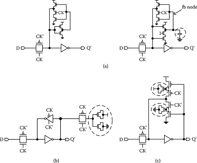
FIGURE 20.1 Node engineering approaches: (a) standard latch design (left) and stack tapering and explicit capacitance addition (right), (b) using a pair of n-type metal–oxide–semiconductor and p-type metal–oxide–semiconductor as extra capacitance, and (c) switched capacitance as extra capacitance. (T. Karnik et al., “Selective node engineering for chip-level soft error rate improvement,” IEEE Symp. VLSI Circuits Dig. Tech. Papers, © 2002 IEEE.)
The DICE design can be understood with an example. Suppose DICE is storing 0 at X0 and X2, and storing 1 at X1 and X3. X0 and X2 are independently controlled, and so are X1 and X3. If one node is upset, for example, X0 changes from 0 to 1, it will turn on N3, changing X3 to 0; turn off P1, leaving X1 floating at 1. X3 will then turn off N2, leaving X2 floating at 0. Therefore, a single-node upset will propagate to only one neighboring node, leaving the remaining two nodes unaffected. The unaffected nodes, X1 and X2, will eventually overcome the upsets by driving X0 low through N0, and driving X3 high through P3.
DICE protects against a single storage node upset. If two nonadjacent nodes are upset, DICE will not be able to recover from it. In the layout of the DICE cell, it is important to keep nonadjacent storage nodes physically separate, and the transistors that are responsible for recovering a storage node should be placed away from the storage node to minimize the impact of multiple-node upsets [19]. Because the error recovery in DICE relies on two floating nodes that can be affected by leakage, it is important to test the DICE circuitry for high leakage that could render the design ineffective. A higher supply voltage reduces recovery time, but it also increases the leakage current that can potentially damage the floating storage nodes during recovery [19]. The choice of the device threshold is also faced with the same trade-off between recovery time and reliability of floating nodes during recovery.
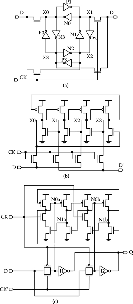
FIGURE 20.2 Dual interlocked storage cell designs. (a) Dual interlocked storage cell structure, (b) dual interlocked storage cell memory cell, and (c) dual interlocked storage cell latch. (T. Calin et al., “Upset hardened memory design for submicron CMOS technology,” IEEE Trans. Nucl. Sci., 43(6), © 1996 IEEE; P. Hazucha et al., “Measurements and analysis of SER-tolerant latch in a 90-nm dual-Vt CMOS process,” IEEE J. Solid-State Circuits, 39(9), © 2004 IEEE.)
The circuit schematic for a DICE memory cell uses only eight transistors, and two or four transistors for access, as shown in Figure 20.2b [18]. A DICE latch can be created similarly as shown in Figure 20.2c [19]. In this design, two output buffers I1 and I2 are attached to the primary and the redundant storage, respectively, to reduce the possible output glitch. When one storage node, for example, N0a, is upset, the resulting glitch in the output of I1 can be balanced by the stable output of I2. Clever layout of this DICE latch results in only a 44% area overhead and a 34% energy overhead for achieving the same timing performance as a standard latch. The DICE latch exhibited 29 times lower SER compared to a standard latch [19].
20.4 Soft-Error Hardened Latch
A particle strike generates electrons and holes. When enough electrons are collected by an n-diffusion, a stored 1 is changed to 0; conversely, when enough holes are collected by a p-diffusion, a stored 0 is changed to 1. The upset is directional: n-diffusion upset is from 1 to 0 only, and p-diffusion upset is from 0 to 1 only. Taking advantage of this fact, a soft-error hardened (SEH) latch is designed to have only three storage nodes for a smaller design [20] as shown in Figure 20.3a. There are three storage nodes: DH, as labeled in Figure 20.3a, stores the inverted D, and PDH and NDH, as labeled in Figure 20.3a, both store D of the same polarity. PDH is tied to p-diffusion only, and NDH is tied to n-diffusion only. When PDH and NDH are storing 0, a particle strike causes PDH to be charged to 1, but NDH remains at 0; when PDH and NDH are storing 1, a particle strike causes NDH to be discharged to 0, but PDH remains at 1. PDH and NDH cannot be upset at the same time.
SEH latch protects against a single storage node upset. Suppose DH stores 1, and PDH and NDH both store 0 (NDH is floating). If PDH is upset and charged to 1, it will turn off P1, leaving DH floating at 1. Q still stays at 0, which keeps N3 off, so that NDH is still floating at 0. NDH and Q keep P2 and P3 on to discharge PDH for error recovery. Suppose DH is upset and discharged to 0, then Q will change to 1. However, it will have no effect on PDH and NDH, except that both PDH and NDH are floating at 0. PDH keeps P1 on to charge DH for error recovery. The error shows up at Q as a 1-glitch. The DH upset recovery time depends on PDH to drive P1 to recover from a 1-to-0 upset. However, PDH stores Vt, a weak 0, which slows down the recovery. Similarly, DH depends on NDH to drive N1 to recover from a 0-to-1 upset, but NDH stores VDD – Vt, a weak 1, that also slows down the recovery.
SEH latch is unable to recover from multiple node upset. However, PDH and NDH cannot be upset simultaneously. PDH and DH can fail at the same time (PDH changes from 0 to 1, and DH changes from 1 to 0), and NDH and DH can also fail at the same time (NDH changes from 1 to 0, and DH changes from 0 to 1). To minimize such possibilities, it is important to keep n-diffusion of DH away from PDH, and p-diffusion of DH away from NDH [20].
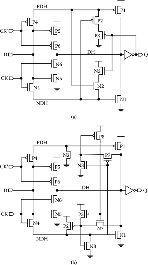
FIGURE 20.3 Soft-error hardened latch designs. (a) Soft-error hardened latch design, and (b) Type-B soft-error hardened latch design. (Y. Arima et al., “Cosmic-ray immune latch circuit for 90nm technology and beyond,” IEEE Int. Solid-State Circuits Conf. Dig. Tech. Papers, © 2004 IEEE; Y. Komatsu et al., “A soft-error hardened latch scheme for SoC in a 90 nm technology and beyond,” Proc. IEEE Custom Integrated Circuits Conf., © 2004 IEEE.)
The incomplete swing of PDH and NDH in SEH latch results in a long recovery time. During steady state, either PDH (when storing 1) or NDH (when storing 0) is floating, and sensitive to leakage and noise coupling. A Type-B SEH latch is designed, as shown in Figure 20.3b [21], to overcome these problems by keeping both PDH and NDH static at full swing. In steady state, N2 and P8 keep PDH static, and N8 and P2 keep NDH static. An upset in P8 can be cancelled by N2, and vice versa. Similarly, an upset in N8 is cancelled by P2, and vice versa. The cancellation lowers the PDH and NDH upset probability. When DH is upset, one of PDH and NDH is floating. However, at full swing, the floating PDH or NDH will drive P1 or N1 to recover DH quickly and a glitch on Q is shortened.
The original SEH latch can be implemented with small area penalty of 15% with almost no increase in power, while its timing performance is 33% worse than a standard latch. It provides 197 times improvement in α-particle immunity and 34 times improvement in neutron immunity, but the recovery time is as long as 3.1 ns [21]. The Type-B SEH latch’s area penalty is higher at 33%. It loses the single error polarity in storage nodes PDH and NDH, so its upset immunity is slightly worse than the original SEH latch: 99 times improvement in α-particle immunity and 25 times improvement in neutron immunity. By keeping storage nodes static and full swing, it allows for a fast recovery time of only 50 ps [21].
20.5 Built-In Soft-Error Resilience
Replacing standard memory cells and latches with custom DICE and SEH cells may be costly. Built-in soft-error resilience (BISER) takes advantage of the built-in scan latches and flip-flops that are already part of many microprocessors, as shown in Figure 20.4a [22,23]. The scan flip-flop is enabled in testing by the two-phase clock SCA and SCB to sample and propagate the test input SI through the scan chain. The test input from the scan flip-flop is loaded to the primary flip-flop by asserting UPDATE. The output of the pipeline stage can be sampled by raising CAPTURE.
BISER makes use of the scan flip-flop as a redundant storage by connecting its data input and clock together with the primary flip-flop. The outputs of the primary and scan flip-flop O3 and O4 are fed to a checker, or C-element, as shown in Figure 20.4b (similarly, the master latch outputs O1 and O2 are also connected to a C-element). The C-element acts as a buffer when O3 and O4 agree, otherwise it blocks O3 and O4, allowing its output Q to retain its previous value. When CK is low, the slave latches are holding data that are subject to upsets. When CK is high, the master latches are holding and are subject to upsets. BISER protects against single latch upset, as the C-element blocks the error propagation. However, BISER fails when two latches, one in the primary flip-flop and one in the scan flip-flop, are upset, as the C-element will pass the error to the output. BISER also prevents the upset of the keeper, because O3 and O4 will drive the C-element to overcome the upset. The C-element needs to be sized stronger than the keeper for the error recovery.
The two flip-flops in BISER are not as tightly coupled as the redundant storage nodes in DICE or SEH latches, and the scan flip-flop can be turned off to save power if the protection is not needed [23]. The scan flip-flop needs to be designed to match the speed of the primary flip-flop, as a slow scan flip-flop will slow down the checking in the C-element and degrade the performance. BISER makes use of intrinsic redundancy, so the area penalty is only 17%. BISER dissipates 2.43 times power for a 20 times improvement in cell-level SER [23].
A potential weakness of BISER is that the combinational C-element is unprotected and vulnerable to SET [24]. When an SET is sampled by latches, it turns into upsets. At a low clock frequency, upsets in latches dominate and BISER remains effective. However, more frequently sampling at a higher clock frequency will likely register more SETs as upsets. If a BISER latch is followed by another BISER latch, as shown in Figure 20.4b [24], the SETs incurred by the C-element of the first BISER latch will be sampled by a pair of latches in the second BISER latch, rendering it completely ineffective. The weakness of BISER is evidenced in particle testing, where it is shown to lose its effectiveness at a higher clock frequency.
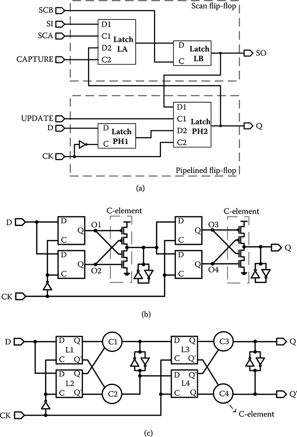
FIGURE 20.4 Built-in soft-error resilience (S. Mitra et al., “Robust system design with built-in soft-error resilience,” Computer, 38(2), © 2005 IEEE; M. Zhang et al., “Sequential element design with built-in soft error resilience,” IEEE Trans. Very Large Scale Integr. (VLSI) Syst., 14(12), © 2006 IEEE.) and bistable cross-coupled dual modular redundancy designs. (J. Furuta et al., “A 65 nm bistable cross-coupled dual modular redundancy flip-flop capable of protecting soft errors on the C-element,” IEEE Symp. VLSI Circuits Dig. Tech. Papers, © 2010 IEEE.) (a) Primary flip-flop and scan flip-flop, (b) built-in soft-error resilience latch design, and (c) bistable cross-coupled dual modular redundancy latch design.
To enhance the reliability of BISER at a high clock frequency, bistable cross-coupled dual modular redundancy (BCDMR) has been invented to harden the C-element using a pair of cross-coupled C-elements, as shown in Figure 20.4c [24]. The cross-coupled C-elements offer a better protection against SET. For example, an SET in C1 will be sampled by L3, but C2 will keep its output stable, so L4 still retains the correct data. In this way, BCDMR improves the SET immunity. It has demonstrated 150 times better SER at a 160 MHz clock frequency than the BISER flip-flop in α-particle testing [24]. The C-elements in BCDMR can be downsized, as the differential drive easily overcomes the keeper. Therefore, the area and power dissipation of BCDMR are comparable to BISER, and the speed of BCDMR is slightly better than BISER.
20.6 Temporal Redundancy Techniques
DICE, SEH, BISER, and BCDMR are based on spatial redundancy: when one copy is perturbed by a particle strike, the redundant copies help it recover. The counterpart of spatial redundancy is temporal redundancy, that is, to record redundant (multiple) samples in time. Because soft errors often last for a short duration, the multiple samples in time enable the detection of transient errors. Error detection is followed by error correction through either re-execution or rollback to the last checkpoint.
The clock-shift temporal redundancy is shown in Figure 20.5a [25], where the output of the combinational circuit is sampled by latch1 that is clocked by CK, and a parallel latch2 that is clocked by a delayed clock CK + δ. To be able to detect an SET pulse of duration up to Ttr, latch2 sampling clock offset δ is set to Ttr + Tsu. A SET pulse of Ttr or shorter is captured by at most one latch, but not both, so the error can be detected by the comparator. The clock-shift design also uncovers SEU occurrence in one of the latches. If δ > 0, the clock-shift design incurs no speed penalty, as latch1 still runs at the same speed using the same clock signal as the unprotected case; whereas latch2 sampling at CK + δ increases the hold time of the combinational circuit by δ. If the fast path in the combinational circuit is tmin < δ, the sampling by latch2 will result in a race condition. A solution to the problem is to pad fast paths by extra delays to ensure that tmin > δ. The clock-shift design requires a delayed clock CK + δ to be distributed, which may be expensive.
An alternative time-shift temporal redundancy is shown in Figure 20.5b [25] to eliminate the delayed clock. In the time-shift design, both latch1 and latch2 sample at CK. The output of the combinational circuit is sampled by latch1, and a δ-delayed output is sampled by latch2. Similar to the previous approach, this design captures two time samples that are spaced by δ. However, the clock period needs to be increased by δ to allow latch2 to sample the slow paths correctly. The time-shift design incurs a speed penalty, but it eliminates race conditions. Time shift is incorporated in the improved BISER [26] and BCDMR designs [24] to improve the protection against SET.
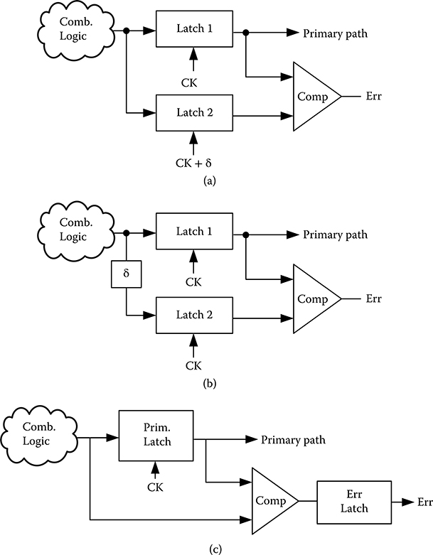
FIGURE 20.5 Temporal redundancy design approaches. (a) Clock-shift temporal redundancy, (b) time-shift temporal redundancy, and (c) transition-detection temporal redundancy. (From M. Nicolaidis, Proc. VLSI Test Symp., 86–94, 1999. With permission; L. Anghel and M. Nicolaidis, “Cost reduction and evaluation of a temporary faults detecting technique,” Proc. Design, Automation and Test in Europe Conf. and Exhibition, 591–598, © 2000 IEEE.)
Both clock-shift and time-shift temporal redundancy designs use two latches and a comparator. A low-cost variation of temporal redundancy, illustrated in Figure 20.5c [27], uses only one latch by comparing the output of latch1 (O1) with its input (O2). The design detects transitions at O2 by comparing it with the latched sample O1. Note that the error flag is only valid during a small window after O1 is sampled and before O2 is overwritten by a fast path, that is, between CK and CK + tmin, so the error flag has to be sampled during this window. To enable detection of an SET pulse of longer than δ, fast paths have to be padded such that tmin > δ. The SEU detection in the transition-detection design is weaker compared to clock-shift or time-shift approaches, because it is only valid between CK and CK + tmin.
20.7 Razor: Double Sampling Sequential Circuits
Razor was invented to detect and correct timing errors caused by supply voltage scaling [28]. With the timing errors corrected by Razor, the supply voltage can be reduced to save power. The circuit schematic of Razor is shown in Figure 20.6a [28], made of a master-slave main flip-flop and a parallel shadow latch. The main flip-flop samples at CK, and the shadow latch samples at a delayed clock CK + δ. An XOR gate compares the samples from the main flip-flop and the shadow latch, and an error is flagged if a mismatch is detected. A Razor flip-flop consumes 66% more energy than a standard flip-flop in an error-free operation at a 10% activity factor. Detecting and correcting an error consumes another 210% more energy [28]. The extra energy in error detection and correction is usually negligible as the error rate is kept low.
Razor’s error detection mechanism follows the clock-shift temporal redundancy approach [25], but Razor was designed to detect timing errors, not soft errors. In the case of timing errors, the worst-case slow path may not meet the timing of the main flip-flop, but it will be correctly sampled by the shadow latch (by design). The correct sample in the shadow latch can be used to correct timing errors. However, in the case of soft errors, soft errors can occur in the main flip-flop or the shadow latch, and there is no guarantee that the shadow latch holds the correct sample. Therefore, Razor can be used for soft-error detection, but not correction.
Razor also incurs possible race conditions due to the delayed sampling by the shadow latch. A longer δ allows more timing errors to be detected and corrected and the supply voltage to be reduced further, but it increases the tmin constraint and delay padding of short paths. Razor is well-suited for critical flip-flops for critical slow paths. In the design demonstrated by D. Ernst et al. [28], Razor was used in 192 critical flip-flops out of a total of 2408 flip-flops, or 8% of the flip-flops, to reduce the cost and minimize the delay padding. However, this approach does not apply if Razor is used for soft-error detection, because soft errors occur in both critical and noncritical paths. Razor needs to be added to all flip-flops for the complete soft-error coverage.
The design of Razor reveals an important metastability issue of temporal redundancy techniques. Because soft errors can occur anytime, it is possible that the data at the input of a latch transitions at the same time as the clock transitions, resulting in a possible metastability [28], where the output is undetermined as it does not settle to either a high or a low voltage level. Metastability gives rise to undetected errors and misdetected errors. Razor incorporates a metastability detector using two parallel inverters [28], inv_n and inv_p shown in Figure 20.6a, whose switching thresholds are skewed low and high, respectively. The two inverters will sample the metastable input and give two different outputs, allowing metastability to be detected. Alternatively, the metastable output can be latched a second time, and the probability that the output of the second latch is metastable becomes negligible. Resolving metastability introduces area and power penalties.
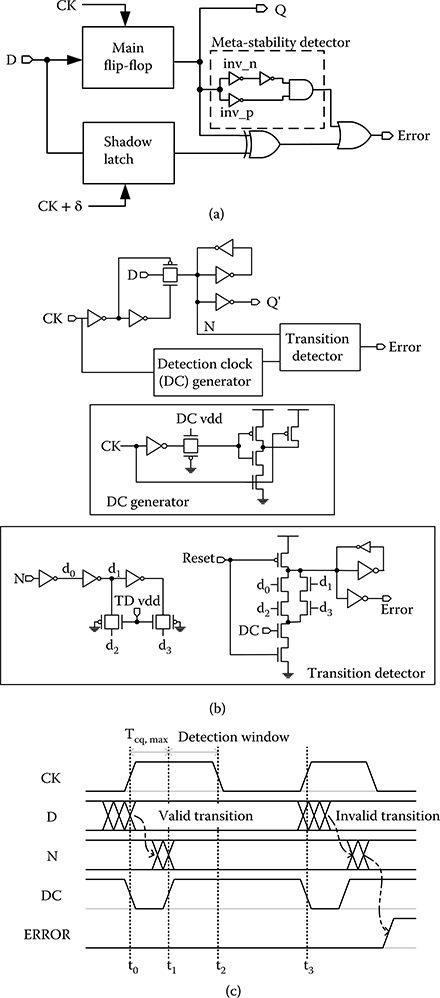
FIGURE 20.6 Razor doubling sampling techniques. (a) Razor flip-flop, (b) Razor II latch, and (c) Razor II timing diagram. (D. Ernst et al., “Razor: a low-power pipeline based on circuit-level timing speculation,” Proc. IEEE/ACM Int. Symp. Microarchitecture, © 2003 IEEE; S. Das et al., “RazorII: in situ error detection and correction for PVT and SER tolerance,” IEEE J. Solid-State Circuits, 44(1), © 2009 IEEE.)
To reduce the area and power of Razor, a low-cost Razor II was introduced [29]. Razor II performs error detection using transition detection as described previously. Razor II removes circuit-level timing error correction, and instead relies on architectural replay for error correction. As the error rate will be kept very low, the cost of architectural replay will be negligible. The schematic of the Razor II latch is shown in Figure 20.6b [29]. The transition detector is attached to the storage node N. The detector creates four copies of N: d0, d1, d2, d3 that are phased apart by an inverter or transmission gate delay (d1, d2 = N; d0, d3 = ~N, the inverted N). The four delayed copies are fed to a dynamic comparator. The comparator is reset high and the error flags false. A transition on node N creates a momentary glitch on d0 first, so that d0 = d2 for a moment; and then the glitch propagates to d1, so that d1 = d3 for a moment, which trigger the discharge of the dynamic comparator and setting the error flag to true.
The transition detection is only enabled after the output of the combinational circuit is correctly sampled by the latch, which occurs by t1, that is, Tcq,max after the rising edge of the clock t0, as illustrated in Figure 20.6c [29]. A detection clock DC disables the transition detector from t0 to t1, so that any errant transition on N for the rest of the clock period will be detected as errors. Razor II latch is able to detect timing errors between t1 and t2, the clock falling edge. The timing error detection window can be adjusted by duty cycling the clock. The metastability detection is removed in this design by ensuring that the latch input never transitions near the clock falling edge. Razor II latch detects soft errors due to SET between t1 and t2, and SEU between t1 and t3, the next clock rising edge. Note that soft errors can cause metastability, which is not detected in this design. The simplified Razor II latch consumes 28.5% more power than a standard latch at a 10% activity factor [29].
20.8 Confidence-Driven Computing
The error detection window of a clock-shift temporal redundancy design, for example, Razor, is limited to δ after the sampling edge, or δ before the sampling edge in a time-shift design. The length of δ determines the error coverage, but it is limited by short paths in a clock-shift design and clock speed in a time-shift design. Using transition detection, for example, in Razor II, the error coverage is widened, but still limited to a fraction of a clock cycle. The error coverage is also fixed in design time and it is difficult to adapt in runtime. Confidence-driven computing (CDC) provides protection against nondeterministic errors over a wide range of rate and duration [30,31]. The concept of CDC is to employ a tunable confidence threshold for an adjustable reliability.
CDC is implemented by placing a confidence estimator (CE) before a pipeline flip-flop, as illustrated in Figure 20.7 [30,31]. CE consists of a flip-flop to store the output of the combinational circuit, a checker to compare the output with the previous sample stored in the flip-flop, and a counter to keep track of the confidence level. The confidence level is raised on an agreement and reset to zero on a disagreement. A controller ensures the confidence level reaches a required threshold before sending a request to the next pipeline stage. When the next pipeline stage becomes ready to accept a new input, an acknowledgement is sent back and the controller enables the pipeline flip-flop to pass the input to the next stage.
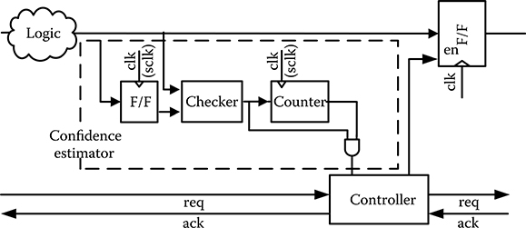
FIGURE 20.7 Design of confidence estimator in confidence-driven computing. (From C. H. Chen et al., “Design and Evaluation of Confidence-Driven Error-Resilient Systems,” IEEE Trans. Very Large Scale Integr. (VLSI) Syst., to be published, © 2013 IEEE.
CDC looks for consecutive agreements in time for error detection and correction. A confidence threshold of n requires n agreements. When an error is detected, the confidence level is reset to 0 and the confidence accumulation starts all over again. The error detection window and the error protection level are adjustable by the confidence threshold, but the throughput is also reduced proportionally. A confidence threshold of n decreases the throughput by n in an error-free operation. Errors decrease the throughput further. However, at a lower error rate, the throughput degradation due to errors is negligible. Experiments show that the error protection can be improved by orders of magnitude with each increment of the confidence threshold by effectively trading off the throughput. The flexibility of CDC comes at a cost of extra area and energy. With a careful design, the area and energy penalty can be limited to as low as 12% and 19%, respectively [30,31].
20.9 Error Resilient System Architecture for Probabilistic Applications
A soft-error resilient system can be constructed bottom-up using hardened circuits as described previously. It is, however, more efficient sometimes to construct a resilient system top-down. For emerging applications, such as estimation, learning, and inference for communications, multimedia, and machine learning, the top-down approach can be especially advantageous. These emerging applications are often computationally intensive and data intensive that require massively parallel architectures. They often deal with noisy inputs from the physical world, and the outputs of these applications have a soft quality metric, for example., in the form of probability, confidence, and bit error rate. The computation is often probability based and the outputs are obtained iteratively. As a result, these emerging applications are intrinsically error resilient.
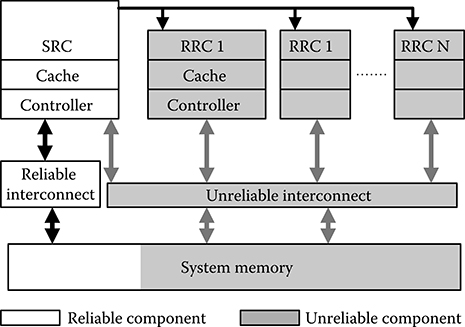
FIGURE 20.8 Error resilient system architecture for probabilistic applications. (H. Cho et al., “ERSA: Error resilient system architecture for probabilistic applications,” IEEE Trans. Comput.-Aided Des. Integr. Circuits Syst,. 31(4), © 2012 IEEE.)
Error resilient system architecture (ERSA), illustrated in Figure 20.8 [32], is a good example of an efficient system architecture that exploits an application’s intrinsic error resilience. ERSA is a multicore architecture that is designed with asymmetric reliability that consists of a small number of highly reliable cores (SRCs) implemented using error hardening techniques, and a large number of less reliable, relaxed reliability cores (RRCs) implemented with minimal error hardening. SRC assigns computation tasks to RRCs and monitor their executions. The overhead of a small number SRC is amortized by a large number RRCs, so the overall overhead remains low. The area overhead of ERSA compared to an unprotected system is only 0.7%, and the power penalty is 1.9% [32].
ERSA uses lightweight execution monitoring, including watchdog timers, memory access boundary monitors, and exception monitors to ensure that the RRCs are responsive, accessing their intended memory block, and reporting unexpected exceptions. When an RRC is stuck and runs into exceptions, the RRC is restarted by the SRC. The monitoring is light weight, as opposed to heavy error detection and correction. The execution monitoring prevents crashes. To ensure the quality of the output, a set of software rules are used to check the validity of the output, damping the fluctuations, and filter out invalid results based on application-specific criteria. These software rules are also light weight and inexpensive to implement.
Experiments have demonstrated that the enhanced ERSA using both execution monitoring and software rule checking achieves significantly better computation accuracies to deliver acceptable outputs. Even as the error rate increases, the execution time on the enhanced ERSA remains low [32]. The cross-layer resilient architecture takes advantage of the application’s error resilience in designing inexpensive hardware. The approach can be a highly cost-effective solution toward the increasingly more complex system design and resiliency problems.
20.10 Commercial Applications of Error Resilient Circuit Designs
The design of the Intel 65-nm Itanium quad-core processor is faced with a reliability challenge due to the triple increase in logic circuits over the previous generation of products, and the requirement of maintaining the same SER [33]. To meet the reliability requirement, the design chose to harden 99% of the latches in the system interface and 33% of the core latches. The DICE structure is incorporated in the pulse latch as shown in Figure 20.9a [33]. The pulse clock PCK enables sampling of the input over a short pulse window. When D = 0, in1 pulls up storage node B and disables the pull up of C, while q1 pulls down C and disables pull down of B. When D = 1, in1 pulls down storage node B and disables the pull down of A, while q2 pulls up A and disables the pull up of B. With the feedback removed, writing is faster than the standard DICE latch by up to 30%, and the clock-to-Q delay matches a standard pulse latch. By separating the diffusions of storage nodes in layout, the DICE pulse latch has demonstrated 100 times lower SER over an unprotected latch with a 34% area penalty and 25% higher active power [33].
A DICE register file design is shown in Figure 20.9b [33]. When bitw = 1, the bit line tries to pull up q and q1, which is facilitated by disabling the pull downs through nq and nq1, making it easier to write 1. When bitw = 0, the design is similar to the standard DICE latch. Therefore, writing 0 is slower than writing 1. The loading on the bit line worsens the write speed. However, write timing is generally not critical for a register file. The DICE register file cell achieves an 80 times lower SER over an unprotected cell with a 25% area penalty and 24% higher standby power [33].
Compared to devices in a bulk CMOS process, silicon-on-insulator (SOI) devices have a thin body. Due to the much smaller charge collection area in the thin body, the upset rate of an SOI device is much lower than bulk devices [34]. To further reduce the upset rate, SOI devices can be electrically connected in series (using separate diffusions that are electrically connected) [35,36]. An upset turns on one device, but it is unlikely for all devices in series to turn on at the same time, thereby preventing an upset of a logic gate.
A stacked transistor approach is adopted in the design of the pulse latch in IBM POWER7TM microprocessor, as shown in Figure 20.9c [37]. Each device in the pulse latch is divided to two devices in a stack with their gates tied together, so it is logically equivalent but provides better upset protection. The transmission gate is not stacked because both sides of the transmission gate are equal for most of the time. An upset turns on the gate without inducing an error. The stacked transistor approach increases the area by less than 10% with only small impact on timing and power. It provides 6 times improvement in SER compared to unprotected bulk devices [37]. The SER of the stacked transistor SOI latch design is comparable to DICE, but its cost is lower than DICE.
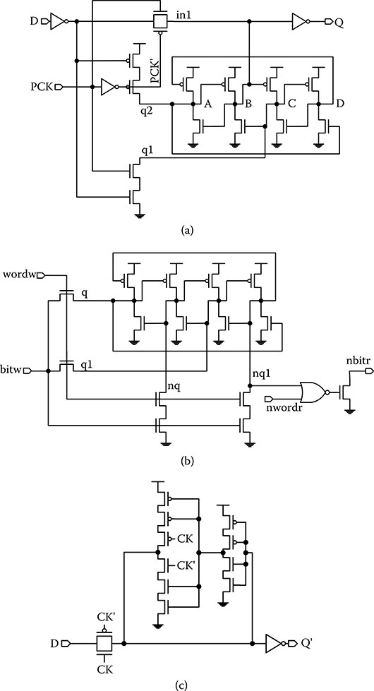
FIGURE 20.9 Applications of hardened latches in commercial microprocessors. (a) Dual interlocked storage cell pulse latch, (b) dual interlocked storage cell register file, and (c) stacked silicon-on-insulator device. (D. Krueger et al. “Circuit design for voltage scaling and SER immunity on a quad-core Itanium processor,” IEEE Int. Solid-State Circuits Conf. Dig. Tech. Papers, © 2008 IEEE; J. Warnock et al., “POWER7 local clocking and clocked storage elements,” IEEE Int. Solid-State Circuits Conf. Dig. Tech. Papers, © 2010 IEEE.)
20.11 Summary
In this chapter, we review circuit design techniques to improve the soft error immunity by leveraging spatial redundancy, temporal redundancy, or architectural adaptation. The redundancy and architectural techniques consume extra area and power, and sometimes degrade the performance. However, each technique can be tailored to specific classes of applications to provide the required level of soft-error protection with the optimal power and overhead cost.
References
1. T. C. May and M. H. Woods, “Alpha-particle-induced soft errors in dynamic memories,” IEEE Trans. Electron Devices, 26(1): 2–9, January 1979.
2. D. Binder, E. C. Smith, and A. B. Holman, “Satellite anomalies from galactic cosmic rays,” IEEE Trans. Nucl. Sci., 22(6): 2675–2680, December 1975.
3. J. F. Ziegler and W. A. Lanford, “Effect of cosmic rays on computer memories,” Science, 206(4420): 776–788, 1979.
4. E. Normand, “Single event upset at ground level,” IEEE Trans. Nucl. Sci., 43(6): 2742–2750, December 1996.
5. P. E. Dodd and L. W. Massengill, “Basic mechanisms and modeling of single-event upset in digital microelectronics,” IEEE Trans. Nucl. Sci., 50(3): 583–602, June 2003.
6. T. Karnik and P. Hazucha, “Characterization of soft errors caused by single event upsets in CMOS processes,” IEEE Trans. Dependable and Secure Computing, 1(2): 128–143, April-June 2004.
7. R. C. Baumann, “Radiation-induced soft errors in advanced semiconductor technologies,” IEEE Trans. Dev. Mat. Rel., 5(3): 305–316, September 2005.
8. JESD. Measurement and reporting of alpha particle and terrestrial cosmic ray-induced soft errors in semiconductor devices, JESD89A, August 2001.
9. P. E. Dodd et al., “Production and propagation of single-event transients in high-speed digital logic ICs,” IEEE Trans. Nucl. Sci., 51(6): 3278–3284, December 2004.
10. P. Hazucha and C. Svensson, “Impact of CMOS technology scaling on the atmospheric neutron soft error rate,” IEEE Trans. Nucl. Sci., 47(6): 2586–2594, December 2000.
11. P. Shivakumar et al., “Modeling the effect of technology trends on the soft error rate of combinational logic,” Proc. Int. Conf. Dependable Syst. and Networks, pp. 389–398, 2002.
12. R. Baumann, “Soft errors in advanced computer systems,” IEEE Design and Test of Comput., 22(3): 258–266, May–June 2005.
13. N. Seifert et al., “Radiation-induced soft error rates of advanced CMOS bulk devices,” Proc. IEEE. Int. Rel. Physics Symp., pp. 217–225, March 2006.
14. P. Roche et al., “A commercial 65 nm CMOS technology for space applications: Heavy ion, proton and gamma test results and modeling,” IEEE. Trans. Nucl. Sci., 57(4): 2079–2088, August 2010.
15. A. Taber and E. Normand, “Single event upset in avionics,” IEEE Trans. Nucl. Sci., 40(2): 120–126, April 1993.
16. T. Karnik et al., “Scaling trends of cosmic ray induced soft errors in static latches beyond 0.18μ,” IEEE Symp. VLSI Circuits Dig. Tech. Papers, pp. 61–62, June 2001.
17. T. Karnik et al., “Selective node engineering for chip-level soft error rate improvement,” IEEE Symp. VLSI Circuits Dig. Tech. Papers, pp. 204–205, Honolulu, HI, June 2002.
18. T. Calin, M. Nicolaidis, and R. Velazco, “Upset hardened memory design for submicron CMOS technology,” IEEE Trans. Nucl. Sci., 43(6): 2874–2878, December 1996.
19. P. Hazucha et al., “Measurements and analysis of SER-tolerant latch in a 90-nm dual-Vt CMOS process,” IEEE J. Solid-State Circuits, 39(9): 1536–1543, September 2004.
20. Y. Arima et al., “Cosmic-ray immune latch circuit for 90nm technology and beyond,” IEEE Int. Solid-State Circuits Conf. Dig. Tech. Papers, pp. 492–493, February 2004.
21. Y. Komatsu et al., “A soft-error hardened latch scheme for SoC in a 90 nm technology and beyond,” Proc. IEEE Custom Integrated Circuits Conf., pp. 329–332, October 2004.
22. S. Mitra et al., “Robust system design with built-in soft-error resilience,” Computer, 38(2): 43–52, February 2005.
23. M. Zhang et al., “Sequential element design with built-in soft error resilience,” IEEE Trans. Very Large Scale Integr. (VLSI) Syst., 14(12): 1368–1378, December 2006.
24. J. Furuta et al., “A 65nm bistable cross-coupled dual modular redundancy flip-flop capable of protecting soft errors on the C-element,” IEEE Symp. VLSI Circuits Dig. Tech. Papers, pp. 123–124, June 2010.
25. M. Nicolaidis, “Time redundancy based soft-error tolerance to rescue nanometer technologies,” Proc. VLSI Test Symp., pp. 86–94, 1999.
26. S. Mitra et al., “Combinational Logic Soft Error Correction,” Proc. IEEE Int. Test Conf., pp. 1–9, October 2006.
27. L. Anghel and M. Nicolaidis, “Cost reduction and evaluation of a temporary faults detecting technique,” Proc. Design, Automation and Test in Europe Conf. and Exhibition, pp. 591–598, 2000.
28. D. Ernst et al., “Razor: a low-power pipeline based on circuit-level timing speculation,” Proc. IEEE/ACM Int. Symp. Microarchitecture, pp. 7–18, December 2003.
29. S. Das et al., “RazorII: in situ error detection and correction for PVT and SER tolerance,” IEEE J. Solid-State Circuits, 44(1): 32–48, January 2009.
30. C.-H. Chen et al., “A confidence-driven model for error-resilient computing,” Proc. Design, Automation and Test in Europe Conf. and Exhibition, pp. 1–6, March 2011.
31. C.-H. Chen et al., “Design and Evaluation of Confidence-Driven Error-Resilient Systems,” IEEE Trans. Very Large Scale Integr. (VLSI) Syst., to be published.
32. H. Cho, L. Leem, and S. Mitra, “ERSA: Error resilient system architecture for probabilistic applications,” IEEE Trans. Comput.-Aided Des. Integr. Circuits Syst., 31(4): 546–558, April 2012.
33. D. Krueger, E. Francom, and J. Langsdorf, “Circuit design for voltage scaling and SER immunity on a quad-core Itanium processor,” IEEE Int. Solid-State Circuits Conf. Dig. Tech. Papers, pp. 94–95, February 2008.
34. A. KleinOsowski et al., “Circuit design and modeling for soft errors,” IBM J. Research and Develop., 52(3): 255–263, May 2008.
35. J. Cai et al., “SOI series MOSFET for embedded high voltage applications and soft-error immunity,” Proc. IEEE Int. SOI Conf., pp. 21–22, October 2008.
36. C. Johnson et al., “A wire-speed power processor: 2.3GHz 45nm SOI with 16 cores and 64 threads,” IEEE Int. Solid-State Circuits Conf. Dig. Tech. Papers, pp. 104–105, February 2010.
37. J. Warnock et al., “POWER7 local clocking and clocked storage elements,” IEEE Int. Solid-State Circuits Conf. Dig. Tech. Papers, pp. 178–179, February 2010.