
2 Signal Processing by Digital Generalized Detector in Complex Radar Systems
2.1 Analog-to-Digital Signal Conversion: Main Principles
For digital signal processing of target return signals in complex radar systems (CRSs), there is a need to carry out an analog-to-digital signal conversion. This transformation is produced by two stages. In the course of the first stage, there is a need to sample the target return signal—the continuous target return signal x(t) is sampled instantaneously and at a uniform rate, once every Ts seconds. In the course of the second stage—quantization—the sampled target return signal {x(nTs)} is converted into a sequence of binary coded words. The sampling and quantization functions are realized by analog-to-digital converters.
The design process of analog-to-digital converters involves particularly the task of choosing a sampling interval value and number of signal quantization levels of the sampled target return signal. Simultaneously, we should take into account the problems of designing and realization both for converters and for digital receivers processing the target return signals. In the present section, we consider and discuss the main aspects and foundations of analog-to-digital signal conversion and the main principles underlying the design of analog-to-digital converters.
2.1.1 SAMPLING PROCESS
In general, a sampling process of the continuous function x(t) representing a target return signal is to measure its values at the time instants spaced Ts seconds apart. Consequently, we obtain an infinite sequence of samples spaced Ts seconds apart and denoted by {x(nTs)}, where n takes on all possible integer values, both positive and negative. We refer to Ts as the sampling period or sampling interval, and to its reciprocal, fs = 1/Ts, as the sampling rate. This ideal form of sampling is called an instantaneous sampling. As a rule, a value of Ts is constant.
A sampling device can be considered as a make circuit with the time τ and sampling period Ts. Time diagram of conversion of the continuous function x(t) into a sequence of instantaneous (τ → 0) readings {x(nTs)} spaced Ts seconds apart is shown in Figure 2.1. Let xδ(t) denote the signal obtained by individually weighting the elements of a periodic sequence of Dirac delta functions spaced Ts seconds apart by the sequence of numbers {x(nTs)} [1]:
xδ(t)=∞∑n=−∞x(nTs)δ(t−nTs).(2.1)
We refer to xδ(t) as the instantaneously (ideal) sampled target return signal. The term δ(t − nTs) represents a delta function positioned at time t = nTs. From the definition of the delta function [2], recall that such an idealized function has unit area. We may, therefore, view the multiplying factor x(nTs) in (2.1) as a “mass” assigned to the delta function δ(t – nTs). A delta function weighted in this manner is closely approximated by a rectangular pulse of duration τ and amplitude x(nTs)/τ; the smaller we make τ, the better the approximation will be.
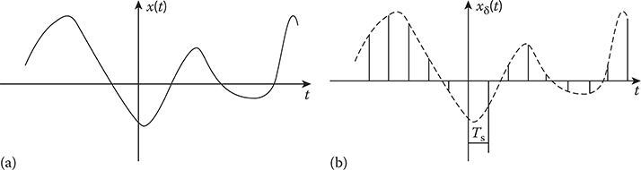
FIGURE 2.1 Illustration of the sampling process: (a) Analog waveform x(t) and (b) instantaneously sampled representation of x(t).
The instantaneously sampled target return signal xδ(t) has a mathematical form similar to that of the Fourier transform of a periodic signal. This is readily established by comparing (2.1) for xδ(t) with the Fourier transform of a periodic signal given by
∞∑m=−∞x(t−mTs)↔fs∞∑n=−∞G(nfs)δ(f−nfs),(2.2)
where G(nfs) is the Fourier transform of x(t), evaluated at the frequency f = nfs. This correspondence suggests that we may determine the Fourier transform of the sampled target return signal xδ(t) by invoking the duality property of the Fourier transform [3], the essence of which is the following:
If x(t)↔G(f),then G(t)↔g(−f).(2.3)
Representation of the continuous function x(t) in the form of the sequence {x(nTs)} is possible only under the well-known restrictions. One restriction in kind is a requirement of spectrum limitation of the sampled target return signal xδ(t). By Kotelnikov’s theorem concerning the signal space concept [4], the continuous target return signal x(t) possessing a limited spectrum is completely defined by countable set of samples spaced Ts ≤ 1/(2fmax) seconds apart, where fmax is the cutoff frequency of target return signal spectrum.
Under digital signal processing in CRSs, a stochastic process at the analog receiver output is an object to sample. This output process is a narrowband process at the condition Δfs/fc ≪ 1, where Δfs is the signal spectrum bandwidth and fc is the carrier frequency. This condition allows us to apply an envelope procedure to represent the narrowband signal in the following form:
x(t)=X(t)cos[2πfct+φ(t)],(2.4)
where
X(t) is the low-frequency signal (envelope)
ϕ(t) is the phase modulation law of the narrowband signal—slowly varied function in comparison with 2πfct
Since information about the target is extracted from the envelope X(t) and phase ϕ(t) of the target return signal and not from the carrier frequency fc, and, moreover, X(t) and ϕ(t) are the slowly varied functions in time, there is a need to convert the target return signal given by (2.4) in such a way that sampling intervals would be defined by the real signal spectrum bandwidth rather then the carrier frequency fc. In the case of the narrowband radio signal, we can write
x(t)=Re[˙X(t)exp(j2πfct)],(2.5)
where Re[·] is the real part of the complex narrowband signal and
˙X(t)=X(t)exp[jφ(t)](2.6)
is the complex envelope of the narrowband signal. This complex envelope of the narrowband signal can be also presented in the following form:
˙X(t)=X(t)cosφ(t)−jX(t)sinφ(t)=x1(t)−jxQ(t),(2.7)
where xI(t) and xQ(t) are, respectively, the in-phase and quadrature components of the narrowband target return signal x(t). Moreover,
X(t)=√x2I(t)+x2Q(t),X(t)>0,(2.8)
φ(t)=arctgxI(t)xQ(t),−π≤φ(t)≤π.(2.9)
The in-phase xI(t) and quadrature xQ(t) components can be obtained by product between the target return signal x(t) and two orthogonal signals with the frequency fc forming at the local oscillator output. The corresponding device is called the phase detector. The flowchart of a simple phase detector is presented in Figure 2.2, where there are multipliers followed by the low-pass filters suppressing all high-frequency harmonics. Thus, the low-pass filters pass only the low-frequency in-phase xI(t) and xQ(t) quadrature components that must be sampled by the analog-to-digital converter.
The complex envelope of the narrowband radio signal can be presented either by the envelope and phase, which are the functions of time, or by the in-phase and quadrature components. In accordance with this statement, under the narrowband radio signal sampling there is a need to use two samples: either the envelope amplitude and phase or the in-phase and quadrature components of complex amplitude of the narrowband radio signal. Thus, we deal with two-dimensional signal sampling.
The sampling theorem for the two-dimensional signal may be presented in the following form [5]
Ts1≤1f1max,Ts2≤1f2max,(2.10)
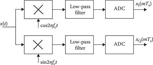
FIGURE 2.2 Example of phase detector: ADC—the analog-to-digital converter.
where f1max and f2max are the highest frequencies in spectra of the first and second components of the narrowband signal. It is important to note that if we represent the narrowband signal using the envelope amplitude and phase, the frequencies then differ: namely, f1max is the maximal frequency of the amplitude-modulated narrowband signal spectrum; f2max is the maximal frequency of the phase-modulated narrowband signal spectrum. For example, in the case of a completely known deterministic signal, the spectral bandwidth of the envelope is defined from the following condition [6,7]:
f1max×τ0=1orf1max=1τ0,(2.11)
where τ0 is the duration of the sampled signal. Consequently, a maximal sampling period of amplitude envelope is limited by the condition Ts ≤ τ0. In doing so, an initial phase of the envelope is known. By this reason, it becomes evident that there is no need to sample it. In the case of a wideband signal of the same duration τ0 (the case of chirp modulation), the spectrum bandwidth of the modulated signal is close to double the amount of frequency deviation [8]:
f2max≈2ΔF0.(2.12)
Consequently, for one-valued representation of the frequency-modulated signal with constant amplitude, there is a need to set the phase
φ(t)=∫ΔF0 dt(2.13)
at readings spaced as
Tsφ≤12ΔF0.(2.14)
Number of phase counts of the signal with duration τ0 is given by
Nφ=2ΔF0τ0.(2.15)
Under the representation of complex envelope of the radio signal in the in-phase xI(t) and quadrature xQ(t) components, the maximal frequencies f1max and f2max are the same, that is,
f1max=f2max=fmax.(2.16)
Consequently, the sampling must be carried out simultaneously over every equal sampling interval:
TsI≤1fmax and TsQ≤1fmax.(2.17)
In the case of the signal with duration τ0 and random initial phase, we can write
fmax=1τ0 and TsI,TsQ≤τ0.(2.18)
In the case of chirp-modulated signal with random initial phase, we have
fmax≈ΔF0(2.19)
Consequently,
TsI,TsQ≤1fmax≤1ΔF0(2.20)
and the number of paired samples for the signal with duration τ0 is determined as
N1,N0=ΔF0τ0.(2.21)
In the case of the phase-manipulated pulse signal, the number of paired samples must not be less than the number of elements in code chain. If τ0 is the duration of elementary signal, then the sampling intervals for the in-phase and quadrature components of the radio signal are given by
TsI,TsQ≤τ0.(2.22)
2.1.2 QUANTIZATION AND SIGNAL SAMPLING CONVERSION
Under digital signal processing of target return signals in CRSs, there is a need to carry out a quantization of sampled values of complex envelope and phase or in-phase and quadrature components of radio signals in addition to sampling. Devices that carry out this function are called the quantizers.
The amplitude characteristic of alternating-sign sample quantizer with a fixed quantization step is presented in Figure 2.3. Here X1, X2, …, Xi, Xi+1, …, Xm are the decision values; X0 is the limiting level of signal; Δx is the quantization step; and x′1,x′2,…,x′m are the sampled data of output signal covering the following center of range:
x′i=Xi+Xi+12.(2.23)
Under quantization of the in-phase and quadrature components of radio signal complex amplitude, the quantization step is chosen, as a rule, based on the condition
Δx=Xmin≤σ0,(2.24)
where σ20 is the variance of receiver noise.
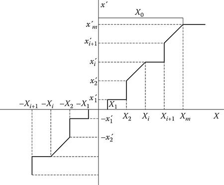
FIGURE 2.3 Alternating—sign sample quantizer with fixed quantization step.
The number of quantization levels is determined by
Nq=Xmax−XminΔx=dr−1,(2.25)
where dr is the dynamic range of analog part of receiver. The number of bit site to represent the sampled target return signal is given by
nb=ℱ[log2(Nq+1)]=ℱ[log2dr],(2.26)
where ℱ[z] is the nearest integer NLE z. To characterize the analog-to-digital converter, we often use the following formula defining a dynamic range in dB for quantized sequence of samples for one bit of conversion [9]:
v=20lgdrnb=20lgdrℱ[log2dr]≈6dBbit.(2.27)
Under detection of the target return signal, definition of its parameters, and noise compensation by digital signal processing subsystems in CRSs, there is a need to use a capacity digit, for example, Nb = 6 ÷ 8, analog-to-digital conversion of the sampled target return signal. Capacity digit quantization at a high sampling rate fs is a very difficult technical problem. Moreover, an increase in the sampling rate fs and capacity digit quantization leads to overdesign of digital signal processing subsystems in complex radar systems. Because of this, we use binary quantizers and binary detectors for target return signals, in addition to capacity digit quantization [10,11]. Binary detectors are very simple under realization by digital signal processing techniques.
2.1.3 ANALOG-TO-DIGITAL CONVERSION; DESIGN PRINCIPLES AND MAIN PARAMETER
Manifold types of analog-to-digital conversion are employed by digital signal processing subsystems in CRSs, for instance, the analog-to-digital conversion of voltage/current, time intervals, phase, frequency, and angular displacement. The principal structure of majority of analog-to-digital converters is the same: There are sampling block, quantization block, and data encoding.
The main engineering data are as follows:
Time parameters defining a speed of operation (see Figure 2.4):
Sampling interval Ts
Time of conversion Tc, within the limits of which the target return signal is processed by the analog-to-digital converter
Time of conversion cycle Tcc, that is, the delay between the instant of appearance of the incoming target return signal at the input of the analog-to-digital converter and the instant of occurrence of output code generation
The number of code bits Nb of the target return signal
The element base of the analog-to-digital converter
Consider in detail the Q-factors or external parameters of analog-to-digital converter.
2.1.3.1 Sampling and Quantization Errors
There are two types of these errors: dynamical errors and statical errors. The dynamical errors are the discrete transform errors. The statical errors are the unit sample errors. The dynamical errors depend on the target return signal nature and time performance of the analog-to-digital converter. The main constituent of this kind of error is an inaccuracy caused by variations in the target return signal parameters at the analog-to-digital converter input. For example, if variations in the amplitude of the target return signal within the limits of Tcc are less or comparable with the quantization step Δx, then
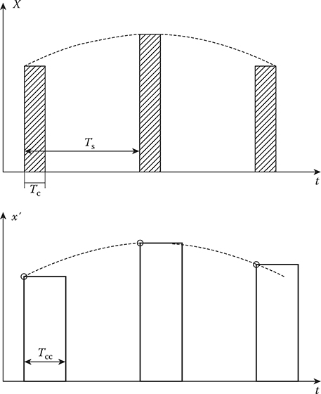
FIGURE 2.4 Time parameters of ADC.
T∝≤ΔxVxmax,(2.28)
where Vxmax is the maximal speed of variations of the sampled and quantized target return signal. Taking into consideration that Tccmax = Ts, we can define the sampling interval Ts based on (2.28).
The unit sample error is caused, first, by quantization error with variance
σ2q=Δx212(2.29)
and, second, by deviation of actual quantization performance from ideal one (see Figure 2.3). If this deviation at the i-th quantization step is equal to ξi and the input target return signal possesses a uniform distribution of instantaneous values within the limits of operating range, then the variance of statical quantization error can be determined by
σ2qΣ=Δx212+1NqNq∑i=1ξ2i.(2.30)
2.1.3.2 Reliability
Reliability of the analog-to-digital converter is the ability to keep operation accuracy at given boundaries within the limits of a definite time interval under a given environment. As a rule, to evaluate the reliability of an analog-to-digital converter the probability of no-failure operation for time t is used, taking into account one of the following failure types:
The outage—glitch
Errors exceed a predefined value of accuracy—degradation failure
Intermittent failure—malfunctions
An increase in the reliability of analog-to-digital converters is obtained owing to redundancy.
Other parameters that pose a risk of limitation include power consumption, weight, and other dimensions of analog-to-digital converters, cost under serial production, manufacturability, time that is required for design, and so on.
As a generalized Q-factor of analog-to-digital converter efficiency, we consider the following ratio:
ℊ=nbfsQ,(2.31)
where
nbfs=nbTs(2.32)
is the data throughput of the analog-to-digital converter and Q is the size of enginery. At the digital signal processing of wideband radio signals in CRSs, rigid requirements in data throughput and reliability are applied to analog-to-digital converters. To design and produce such converters, the parallel Fourier transforms for target return signals are used.
2.2 Digital Generalized Detector For Coherent Impulse Signals
2.2.1 MATCHED FILTER
Recall briefly the main statements of classical detection theory. In accordance with a general theory of radar signal processing, the signal processing in time of stochastic process x(t) representing an additive mixture of the signal s(t) and stationary white Gaussian noise w(t) is reduced to calculation of the correlation integral, which in the case of a scalar real signal s(t, α) with known parameter α can be presented in the following form:
T(α)=∞∫−∞s*(t,α)x(t)dt,(2.33)
where s*(t, α) is the expected signal model generated by a local oscillator in the receiver or detector. If α is the delay of the expected signal with respect to the incoming initial input realization x(t), then the correlation integral is determined as
T(α)=∞∫−∞s*(t−α)x(t)dt.(2.34)
Equation 2.34 is analogous to the convolution integral describing a process at the linear system output with impulse response h(t) if the stochastic process x(s) comes in at the linear system input:
Z(t)=∞∫−∞h(t−s)x(s)ds.(2.35)
This analogy allows us to use the linear filter to calculate the correlation integral, the impulse response of which is matched with the expected signal s(t). Matching is reduced to choice of a corresponding linear filter impulse response satisfying the following condition:
T(t0+α)=Z(α).(2.36)
For the considered case of detection problem the impulse response of the matched linear filter must be mirrored with respect to the expected signal
h(t)=as(t0−t),(2.37)
where
t0 is the delay of signal peak at the matched filter output, which in the case of the pulse signal must be t0 ≥ τ0
a is the fixed scale factor
If the process x(t) = s(t, α) + w(t) comes in at the matched filter input, then according to (2.36) the process forming at the matched filter output at the instant t0 = τ0 is defined in line with the following formula:
Z(t)=a∞∫t−τ0x(u)s*(τ0−t+u)du.(2.38)
In particular, when w(t) = 0, we obtain
Z(t)=a∞∫t−τ0s(u)s*(τ0−t+u)du=aRss*(τ0−t),(2.39)
where Rss*(τ0 − t) is the autocorrelation function of expected signal s(t, α).
As it follows from (2.38) and (2.39), the signal at the matched filter output coincides with the mutual correlation function of the signal model and expected signal accurate within the fixed factor. When the white noise is absent, that is, w(t) = 0, the output signal coincides with the same accuracy with the autocorrelation function Rss*(τ0 − t) of expected signal s(t, α) at the time instant (τ0 − t). Signal-to-noise ratio (SNR) by energy at the matched filter output is given by
SNR=2EsN0,(2.40)
where 0.5N0 is the two-sided power spectral density of white noise. The Neyman-Pearson detector brings us the analogous results [12]. Thus, the matched filter allows us to obtain the maximal SNR at the output within the limits of classical signal detection theory. Realization of analog matched filters in practice is very difficult, especially in the case of wideband signals. Moreover, it is impossible to carry out a parameter tuning for analog matched filters. For this reason, digital matched filters are widely used.
2.2.2 GENERALIZED DETECTOR
Recall the main functioning principles of the generalized detector (GD) constructed based on the generalized approach to signal processing in noise [13-17]. The GD is a composition of the linear systems, Neyman-Pearson receiver, and energy detector. A flowchart of a GD explaining the main functioning principles is shown in Figure 2.5. Here, we use the following notations: the model signal generator or local oscillator (MSG), the preliminary linear system or filter (PF), and the additional linear system of filter (AF).
Consider briefly the main statements regarding AF and PF. There are two linear systems at the GD front end that can be presented, for example, as bandpass filters, namely, the PF with the impulse response hPF(τ) and the AF with the impulse response hAF(τ). For simplicity of analysis, we consider that these filters have the same values for amplitude-frequency responses and band-widths. Moreover, a resonant frequency of the AF is detuned relative to a resonant frequency of the PF on such a value that the incoming signal cannot pass through the AF. Thus, the received signal and noise can appear at the PF output and the only noise appears at the AF output (see Figure 2.5).

FIGURE 2.5 Generalized detector.
It is a well-known fact that if a value of detuning between the AF and PF resonant frequencies is more than 4 ÷ 5Δfs, where Δfs is the signal bandwidth, the processes forming at the AF and PF outputs can be considered as independent and uncorrelated processes. In practice, the coefficient of correlation is not more than 0.05. In the case of signal absence in the input process, the statistical parameters at the AF and PF outputs will be the same under the condition that these filters have the same amplitude-frequency responses and bandwidths by value, because the same noise is coming in at the AF and PF inputs. We may think that the AF and the PF do not change the statistical parameters of input process, since they are the linear front-end systems of a GD. For this reason, the AF can be considered as a generator of reference sample with a priori information a “no” signal is obtained in the additional reference noise forming at the AF output.
There is a need to make some comments regarding the noise forming at the PF and AF outputs. If the white Gaussian noise with zero mean and finite variance σ2n comes in at the AF and PF inputs, the linear front-end system of the GD, the noise forming at the AF and PF outputs is Gaussian, too, because AF and PF are the linear systems and, in general, the noise takes the following form:
ξPF(t)=∞∫−∞hPF(τ)w(t−τ)dτandξAF(t)=∞∫−∞hAF(τ)w(t−τ)dτ,(2.41)
where ξPF(t) and ξAF(t) are the narrowband Gaussian noise. If, for example, the additive white Gaussian noise with zero mean and two-sided power spectral density 0.5N0 is coming in at the AF and PF inputs, then the noise forming at the AF and PF outputs is Gaussian with zero mean and variance given by [14, pp. 264–269]
σ2n=N0ω208ΔF,(2.42)
where if the AF or the PF is the RLC oscillator circuit, then the AF or the PF bandwidth ΔF and resonance frequency ω0 are defined in the following manner:
ΔF=πβ,ω0=1√LC,where β=R2L.(2.43)
The main functioning condition of a GD is the equality over the whole range of parameters between the expected signal s(t, α) and the model signal forming at the MSG or local oscillator output s*(t − τ0, a). How we can satisfy this condition in practice is discussed in detail in Refs. [14, pp. 669-695, 17]. More detailed discussion about choosing between the PF and the AF and their amplitude-frequency responses is given also in Refs. [15,16].
According to Figure 2.5 and the main functioning principle of a GD, the process forming at the GD output takes the following form:
ZoutGD(t)=aRss*(τ−t)+ξ2AF(t)−ξ2PF(t).(2.44)
From (2.44) we see that the signal at the GD output coincides with the mutual correlation function of the signal model and expected signal accurate within the fixed factor. In a statistical sense, the background noise ξ2AF(t)−ξ2PF(t) forming at the GD output tends to approach zero when the number of samples or the time interval of observation tends to approach infinity [15,17]. SNR by energy at the GD output is given by [14]
SNR=Es√4σ4n=Es2σ2n,(2.45)
where σ2n is defined by (2.42).
2.2.3 DIGITAL GENERALIZED DETECTOR
Now consider briefly the main principles of designing and construction of the digital GD (DGD). The DGD flowchart is represented in Figure 2.6. We see that processes at the outputs of MSG, PF, and AF are sampled and quantized, which is equivalent to passing these processes through digital filters. The model signal forming at the MSG output after sampling and quantization can be presented in the following form:
s*(lTs)=aTss*[(n0−l)Ts],(2.46)
where n0 = τ0/Ts is the number of discrete elements of the model signal. For simplicity, we can assume that a=T−1s. Then
s*(lTs)=s*[(n0−l)Ts],(2.47)
where l = (0, 1,…, n0 − 1).
If the main functioning condition of GD, that is, an equality over the whole range of parameters between the expected signal s(t, α) and the model signal forming at the MSG output s*(τ0 − t + u) is satisfied, the process at the DGD output, when the additive mixture of the signal s(t) and stationary white Gaussian noise w(t) comes in at the input, can be represented in the following form [18–21]:
ZoutDGD(kTs)=2n0−1∑l=0C(l)x[(k−l)Ts]s*[(n0−l)Ts]−n0−1∑l=0C(l)x2[(k−l)Ts]+n0−1∑l=0C(l)ξ2AF[(k−l)Ts],(2.48)
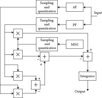
FIGURE 2.6 Digital generalized detector.
where
{x[(k−l)Ts]=x(t)|t=τ0;s*[(n0−l)Ts]=s*(t)|t=τ0;s[(n0−l)Ts(t)]|t=τ0;ξPF[(k−l)Ts]=ξPF(t)|t=τ0;ξAF[(k−l)Ts]=ξAF(t)|t=τ0(2.49)
and
C(l)=TsC0(l)(2.50)
are the coefficients determined by numerical integration using the technique of rectangles (any technique may be used):
C0(l)=1,1,…,1,0.(2.51)
If in (2.48) we replace n0 − l by i in the first term, after elementary mathematical transformations of the first term with the second term we obtain
Rss*(kTs)=∑is*(iTs)s[(k−(n0−i))Ts].(2.52)
Equation 2.52 represents, by analogy with (2.39), the autocorrelation function of the expected signal s(t, α). The autocorrelation function (2.52) of the signal at the DGD output is a periodic function by frequency. At low values of fs, cross-sections of the autocorrelation function (2.52) may overlap, which leads to distortions of the process forming at the DGD output. However, if fs were chosen in agreement with the sampling theorem, these distortions would be negligible.
As it follows from (2.52), when the expected signal s(iTs) comes in at the DGD input, the signal at the DGD output is matched with the autocorrelation function (2.52) accurate within the cofactor aTs. Since the autocorrelation function (2.52) is symmetric with respect to its maximum Rss*(0), the data samples of the sequence {ZoutGD(kTs)} at the DGD output will at first increase and after reaching the upper limit at kTs = n0Ts, that is, the maximal value of the autocorrelation function (2.52), decrease to zero within the limits of the time interval between n0Ts and 2n0Ts. The envelope of the data samples of the sequence {ZoutGD(kTs)} at the DGD output coincides with an envelope of the autocorrelation function Rss*(kTs) given by (2.52). This peculiarity of data samples of the sequence {ZoutGD(kTs)} at the DGD output agrees with that of analog GD.
The limiting value of the DGD output signal energy is equal to the energy of expected signal sequence s(kTs) and is reached at the finite signal bandwidth and Ts ≤ (2Δfs)-1, where Δfs is the signal bandwidth. If the signal spectrum is infinite and we must take into account some effective signal bandwidth Δfeffs under sampling, there are energy losses owing to superposition of unaccounted power spectral density tails under their mutual shift on k/Ts. These energy losses may be taken into consideration introducing an additional noise within the power spectral density 0.5N′0. The receiver noise of DGD is the stationary random sequence with the power spectral density 0.5N″0 uniform within the limits of the bandwidth −(2Ts)−1 ≤ Δf < (2Ts)-1 and depends on Ts.
It is well known that the sampling and quantization techniques are used to digitize analog signals. For example, the sampling technique is used to discretize a signal within the limits of the time interval, and the quantization technique is used to discretize a signal by amplitude within the limits of the sampling interval. For this reason, there is a need to distinguish between the errors caused by these two digitizing techniques, which allows us to obtain a high accuracy of receiver performance. Amplitude quantization and sampling can be considered as additional noises ζ1(kTs and ζ2(kTs) with zero mean and finite variances σ2ζ1 and σ2ζ2, respectively. If the relationship between the chosen amplitude quantization step Δx and the mean square deviation σ′ of process at sampling, and quantization block output is determined by Δx < σ′, then the absolute value of mutual correlation function between the amplitude quantization error and the signal is approximately 10-9 with respect to the values of the autocorrelation function of the signal. Therefore, it is reasonable to neglect this mutual correlation function. As a first approximation, it is reasonable to assume that the noises ζ1(kTs) and ζ2(kTs) are Gaussian.
We may suggest that the additive component ζ∑(kTs) can be presented in the form of summary uncorrelated interferences: the interference caused by quantization ζ1(kTs), normal Gaussian with zero mean and the finite variance σ2ζ1, and the interference caused by sampling ζ2(kTs), normal Gaussian with zero mean, and the finite variance σ2ζ1. Thus, the summary additive interference ζ2(kTs) can be presented in the following form:
ζΣ(kTs)=ζ1(kTs)+ζ2(kTs)(2.53)
and is the normal Gaussian with zero mean and the finite variance given by
σ2ζΣ=σ2ζ1+σ2ζ2(2.54)
This is a direct consequence of Bussgang’s theorem [22].
Taking into consideration the aforementioned statements, the total background noise at the DGD output is defined by the receiver noise and interferences caused by quantization and sampling:
the total background noise=ξ2AFΣ(kTs)−ξ2PFΣ(kTs),(2.55)
where
ξPFΣ(kTs)=ξPF(kTs)+ζΣ(kTs)=ξPF(kTs)+ζ1(kTs)+ζ2(kTs)(2.56)
is the noise forming at the PF output of DGD input linear system consisting of the normal Gaussian noise ξPF(kTs) with zero mean and the variance σ2n; the interference ζ1(kTs) with zero mean and the variance σ2ζ1, which is caused by quantization; and the interference ζ2(kTs) with zero mean and the variance σ2ζ2, which is caused by sampling. Noise πPF(kTs) and interferences ζ1(kTs) and ζ2(kTs) do not correlate with each other.
ξAFΣ(kTs)=ξAF(kTs)+ζΣ(kTs)=ξAF(kTs)+ζ1(kTs)+ζ2(kTs)(2.57)
is the noise forming at the AF output of DGD input linear system (additional or reference noise) [14,17-21], consisting of the normal Gaussian noise ξAF(kTs) with zero mean and the variance σ2n; the interference ζ1(kTs) with zero mean and the variance σ2ζ1, which is caused by quantization; and the interference ζ2(kT2) with zero mean and the variance σ2ζ2, which is caused by sampling. The noise ξAF(kTs) and the interferences ζ1(kTs) and ζ2(kTs) do not correlate to each other.
The probability density function of the total background noise forming at the DGD output is symmetric with respect to zero because the means of noises ξPF(kTs) and ξAF(kTs) and interferences ζ1(kTs) and ζ2(kTs) are equal to zero owing to the initial conditions. The probability density function of the total background noise forming at the DGD output is discussed in detail in Refs. [14, pp. 250-263,15]. Because the noise ξPF(kTs) and ξAF(kTs) and the interferences ζ1(kTs) and ζ2(kTs) do not correlate with each other, the variance of the total background noise and the interferences forming at the DGD output can be determined in the following form [18-21]:
σ2ξ2AFξ−ξ2PFξ=4σ4n+4σ4ζΣ.(2.58)
SNR by energy at the DGD output is given by the following [14, pp. 504-508, 18-21]:
SNR=Es√σ2ξ2AFΣ−ξ2PFΣ=Es√4σ4n+4σ4ζΣ=Es2√σ4n+σ4ζΣ,(2.59)
where σ2n is defined by (2.42) and σ2ζΣ is given by (2.54).
Thus, the losses caused by the sampling period Ts are possible in digital signal processing subsystems employed by complex radar systems.
2.3 Convolution in Time Domain
Target return signals employed by CRSs typically have a narrowband. It is for this reason the DGD must use two channels for signal processing: in-phase and quadrature channels. The narrowband target return signals coming in at the input of DGD linear systems can be presented by the in-phase xI[k] and quadrature xQ[k] constituents at discrete sampling instants kTs. In this case, the complex envelope of the input signal can be presented in the following form:
˙X[k]=xI[k]−jxQ[k].(2.60)
By analogy with (2.60), the complex envelope at the output of the MSG can be presented in the following form:
˙S*[k]=S*I[k]+jS*Q[k].(2.61)
The process at the DGD output accurate within the factor 0.5Ts can be determined in the following form [19]:
ZoutDGD[k]=2˙X[k]˙S*[k]−˙X2[k]+ξ2AF[k],(2.62)
where ξAF[k] is the noise forming at the AF output (the input linear filter of DGD). We can discard the third term in (2.62) and will consider it in the end result. Based on (2.61) and (2.62), the process at the DGD output can be written as follows:
ZoutDGD[k]=2{[xI[k]−jxQ[k]][S*I[k]+jS*Q[k]]}−{xI[k]−jxQ[k]}2=n0−1∑l=0{2{[xI[k−l]−jxQ[k−l]][S*I[n0−l]+jS*Q[n0−1]]}−{xI[k−l]−jxQ[k−l]}2}.(2.63a)
Replacing n0 − l by i in (2.63a), we obtain
ZoutDGD[k]=n0−1∑l=0{2{{xI[k−(n0−i)]−jxQ[k−(n0−i)]}{S*I[i]+jS*Q[i]}}−{xI[k−(n0−i)]−jxQ[k−(n0−i)]}2}.(2.63b)
According to the analysis carried out in [15, pp. 269-282] and following the main functioning DGD condition, that is, in the considered case
S*I(i)=SI[k−(n0−i)]andS*Q(i)=SQ[k−(n0−i)],(2.64)
the in-phase and quadrature constituents of the process at the DGD output can be presented in the following form:
ZoutDGDI=ZoutDGDII+ZDoutGDQQ=S*I(i)SI[k−(n0−i)]−ξ2I[k−(n0−i)]+S*Q(i)SQ[k−(n0−i)]+ξ2Q[k−(n0−i)],(2.65)
ZoutDGDQ=ZoutDGDIQ+ZoutDGDQI=−4S*I(i)SQ[k−(n0−i)]−4S*I(i)ξQ[k−(n0−i)]+4S*Q(i)SI[k−(n0−i)]+4S*Q(i)ξI[k−(n0−i)]+2ξQ[k−(n0−i)]ξI[k−(n0−i)],(2.66)
where the factor 2 in the second line is caused by the presence of amplifier (see Ref. [15, pp. 269-282]). Moreover, the corresponding terms in the first and second lines of (2.66) are compensated in the statistical sense. As a result, the quadrature constituent of the process at the DGD output is caused by the autocorrelation function of the in-phase and quadrature constituents of the narrowband noise. Thus, we can write
RZoutDGGQ(τ)=σ2ξ2AFΣ−ξ2PFΣΔF sinc(ΔFτ),(2.67)
where the variance of the total background noise at the DGD output σ2ξ2AFΣ−ξ2PFΣ is given by (2.58); the DGD input linear system (PF and/or AF) bandwidth is defined by (2.43); and sinc(x) is the sinc function [1].
Further specification of digital signal processing algorithms is defined by type of convolved signals. For example, in the case of chirp modulation of the signal with rectangular envelope
S(t)=sin[2πfct+γt2],(2.68)
where 0 < t ≤ τ0 and γ = πΔF0/τ0 = const; ΔF0 is the target return signal frequency deviation. The complex envelope can be presented in the following form:
˙S(t)=sinγt2−jcosγt2.(2.69)
Consequently, the in-phase and quadrature constituents of the target return signal at discrete instants. [k − (n0 − i)]Ts can be presented in the following form:
{xI[k−(n0−i)]=sinγ[k−(n0−i)]2+ξI[k];xQ[k−(n0−i)]=cosγ[k−(n0−i)]2+ξQ[k],(2.70)
where ξI[k] and ξQ[k] are the constituents of the narrowband noise forming at the PF (the DGD input linear system) output.
In this case, the complex envelope of the model signal forming at the MSG output takes the following form:
˙S*(τ0−t)=sin[γ(τ0−t)2]+jcos[γ(τ0−t)2],(2.71)
and the in-phase and quadrature constituents at discrete instants iTs are given by
S*I[i]=sinγ[i]2andS*Q[i]=cosγ[i]2(2.72)
The flowchart of the generalized signal processing algorithm given by (2.62) is shown in Figure 2.7. There are eight convolving blocks and six summators to calculate all in-phase and quadrature constituents of the process forming at the DGD output. Each in-phase and quadrature components can be presented in the following form taking into account (2.68) through (2.72):
ZoutDGDΠ=2n0∑i=1sinγ[i]2xI[k−(n0−i)]=2n0∑i=1sinγ[i]2sinγ[k−(n0−i)]2+2n0∑i=1sinγ[i]2ξI[k−(n0−i)]2;(2.73)
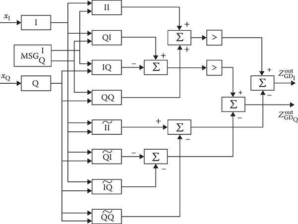
FIGURE 2.7 Convolution in time using the digital generalized detector.
ZoutDGDQQ=2n0∑i=1cosγ[i]2xQ[k−(n0−i)]=2n0∑i=1cosγ[i]2cosγ[k−(n0−i)]2+2n0∑i=1cosγ[i]2ξQ[k−(n0−i)]2;(2.74)
ZoutDGDQI=2n0∑i=1cosγ[i]2xI[k−(n0−i)]=2n0∑i=1cosγ[i]2sinγ[k−(n0−i)]2+2n0∑i=1cosγ[i]2ξI[k−(n0−i)]2;(2.75)
ZoutDGDIQ=2n0∑i=1sinγ[i]2xQ[k−(n0−i)]=2n0∑i=1sinγ[i]2cosγ[k−(n0−i)]2+2n0∑i=1sinγ[i]2ξQ[k−(n0−i)]2;(2.76)
˜ZoutDGDΠ=∑n0i=1xI[k−(n0−i)]xI[k−(n0−i)]=∑n0i=1{sinγ[k−(n0−i)]2+ξI[k−(n0−i)]}×∑n0i=1{sinγ[k−(n0−i)]2+ξI[k−(n0−i)]}=∑n0i=1sin2γ[k−(n0−i)]2+2∑n0i=1sinγ[k−(n0−i)]2ξI[k−(n0−i)]+∑n0I=1ξ2I[k−(n0−i)];(2.77)
˜ZoutDGDQQ=∑n0i=1xQ[k−(n0−i)]xQ[k−(n0−i)]=∑n0i=1{cosγ[k−(n0−i)]2+ξQ[k−(n0−i)]}×∑n0i=1{cosγ[k−(n0−i)]2+ξQ[k−(n0−i)]}=∑n0i=1cos2γ[k−(n0−i)]2+2∑n0i=1cosγ[k−(n0−i)]2ξQ[k−(n0−i)]+∑n0i=1ξ2Q[k−(n0−i)];(2.78)
ZoutDGDQI=n0∑i=1xQ[k−(n0−i)]xI[k−(n0−i)]=n0∑i=1{cosγ[k−(n0−i)]2+ξQ[k−(n0−i)]}×n0∑i=1{sinγ[k−(n0−i)]2+ξI[k−(n0−i)]}=n0∑i=1cosγ[k−(n0−i)]2sinγ[k−(n0−i)]2+n0∑i=1cosγ[k−(n0−i)]2ξI[k−(n0−i)]+n0∑i=1sinγ[k−(n0−i)]2ξQ[k−(n0−i)]+n0∑i=1ξQ[k−(n0−i)]ξI[k−(n0−i)];(2.79)
ZoutDGDIQ=n0∑i=1xI[k−(n0−i)]xQ[k−(n0−i)]=n0∑i=1{sinγ[k−(n0−i)]2+ξI[k−(n0−i)]}×n0∑i=1{cosγ[k−(n0−i)]2+ξQ[k−(n0−i)]}=n0∑i=1sinγ[k−(n0−i)]2cosγ[k−(n0−i)]2+n0∑i=1sinγ[k−(n0−i)]2ξI[k−(n0−i)]+n0∑i=1cosγ[k−(n0−i)]2ξI[k−(n0−i)]+n0∑i=1ξI[k−(n0−i)]ξQ[k−(n0−i)].(2.80)
In the case of the phase-code-manipulated signal with duration τ∑0 = Neτ0, where Ne is the number of elementary signals and τ0 is the duration of elementary signal, the complex amplitude envelope can be presented in the following form:
˙S(t)=Ne∑i=1˙Si(t),where˙Si(t)=exp(jθi).(2.81)
In the case of binary signal, we have θi = [0, π] and
˙Si(t)=ς[i]=±1.(2.82)
Consequently, the discrete impulse response at the MSG output matched with the phase-code-manipulated target return signal is given by
S*[i]=ς[Ne−i](2.83)
and the in-phase and quadrature constituents of process forming at the DGD output take the following form:
{ZoutDGDI2[k]=Ne∑i=1{ς[Ne−i]ς[k−(Ne−i)]}2+Ne∑i=1{ξ2AFI[k−(Ne−i)]−ξ2PFI[k−(Ne−i)]}2;ZoutDGDQ2[k]=Ne∑i=1{ς[Ne−i]ς[k−(Ne−i)]}2+Ne∑i=1{ξ2AFQ[k−(Ne−i)]−ξ2PFQ[k−(Ne−i)]}2,(2.84)
where the complex amplitude envelope of the DGD output process is defined as follows:
ZoutDGD2[k]=√ZoutGDI2[k]+ZoutGDQ2[k].(2.85)
Thus, in the case of the phase-code-manipulated target return signal, the DGD employed by digital signal processing subsystem in complex radar system uses only four convolving blocks. Moreover, a convolution within the limits of each cycle equal to the elementary signal duration τ0 is a summation of amplitude samples of the in-phase and quadrature constituents of the target return signal at instants with signs defined by values S*[i] = ±1 in accordance with the given code of the phase-manipulated operation. Practical realization of this principle is not difficult.
Now consider the flowchart shown in Figure 2.7 and estimate a functional ability of DGD with convolution blocks in time domain to compress the chirp-modulated target return signal. As we can see from Figure 2.7, we use eight convolving blocks. Each convolving block must carry out n0 multiplications and n0 − 1 additions of Nb numbers in the course of calculation of the k-th signal value, that is, within the limits of the sampling interval Ts. Estimate a required processing speed of the convolving block, taking into account only multiplications for the widely used case of signal processing of the chirp-modulated target return signals at the sampling rate fs = ΔF0 and the target return signal duration τ0 = n0Ts, namely, Vreq = n0ΔF0. For example, when n0 = 100 and ΔF0 = 5 × 10⁶ Hz, the required processing speed must be about Vreq = 5 × 10⁸ multiplications per second.
Consequently, in the considered case, a direct realization of convolution operations by serial digital signal processing techniques is not possible. There is a need to apply specific procedures of calculations under digital signal processing. First of all, we may use a principle of parallelism that is characteristic of convolution problems. This principle allows us to calculate n0 of pairwise multiplications S*[i] × x[k − (n0 − i)], where i = 1,…, n0, simultaneously using n0 parallel multipliers with subsequent summation of partial multiplications (see Figure 2.8). In this case, each multiplier must possess the processing speed Vreq = 5 × 10⁶ multiplications per second, that is, one multiplication operation per 40 ns. This processing speed can be easily provided by employing very large-scale integration (VLSI) circuits.
Another example of accelerated convolution operation is the implementation of a specifically designed processor that uses the read-only memory (ROM) block to store calculations of bitwise multiplications made before. Factor codes are used as result addresses of these bitwise multiplications [22,23]. Consider in detail the convolution principle carried out by a specific processor with ROM. For this case, we can present the process at the DGD output as a convolution operation in the following form to simplify calculations:
ZoutDGD=2N∑i=1S*iXi−N∑i=1X2i+N∑i=1ξ2AFi,(2.86)
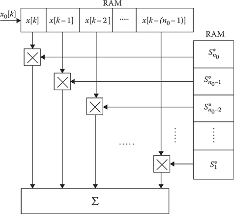
FIGURE 2.8 Principle of parallelism: RAM—the random access memory.
where
S*i can be considered as the weight factors of the model signal at the MSG output
Xi is the sample of the input target return signal
N is the sample size
We can assume that the input target return signals are scaled and as a sequence, |Xi| < 1. In addition, the input target return signals are presented in the form of n-bit additional comma-fixed code. Then (2.86) can be presented in the following form:
ZoutDGD=2N∑i=1S*i(ni∑i=1X(k)i2−k−X(0)i)−(ni∑k=1X(k)i2−k−X(0)i)(ni∑i=1X(k)i2−k−X(0)i)+(ni∑k=1ξ(k)AFi2−k−ξ(0)AFi)(ni∑k=1ξ(k)AFi2−k−ξ(0)AFi),(2.87)
where X(k)i and ξ(k)i are the values (0 or 1) of k-th bit of i-th sample of the input signal.
The DGD output process given by (2.87) can also be presented in the following form:
ZoutDGD=n−1∑k=12−k[2(N∑i=1S*iX(k)i−N∑i=1S*iX(0)i)−(N∑i=1X(k)i−N∑i=1X(0)i)(N∑i=1X(k)i−N∑i=1X(0)i)+(N∑i=1ξ(k)AFi−N∑i=1ξ(0)AFi)(N∑i=1ξ(k)AFi−N∑i=1ξ(0)AFi)].(2.88)
Now we can introduce the function Gk with N binary arguments in the following form:
Gk(X(k)1,X(k)2,…,X(k)N)=2N∑i=1S*iX(k)i−N∑i=1X(k)iN∑i=1X(k)i+N∑i=1ξ(k)AFiN∑i=1ξ(k)AFi.(2.89)
In this case, (2.88) takes the following form:
ZoutDGD=n−1∑k=12−kGk(X(k)1,X(k)2,…,X(k)N)−G0(X(0)1,X(0)2,…,X(0)N).(2.90)
Since arguments of the function Gk(X(k)1,X(k)2,…,X(k)N) can possess the value 0 or 1, the function Gk(X(k)1,X(k)2,…,X(k)N) is characterized by the finite number 2N of its values that can be calculated before and stored by the ROM. Now, the values of bits of the input target return signal X(k)1,X(k)2,…,X(k)N can be used for ROM addressing to choose corresponding values of the function Gk(X(k)1,X(k)2,…,X(k)N). Henceforth, these values will be used to determine the DGD output process ZoutDGD by (2.90).
Thus, a convolution of the DGD output process ZoutDGD can be obtained by n addressing to ROM, n − 1 summations, and the only subtraction (k = 0). In doing so, a number of operations occur independent of the sample size N and are determined by quantization bits of the input target return signals. A very simple block diagram of a specifically designed processor that produces a convolution in accordance with (2.90) is presented in Figure 2.9.
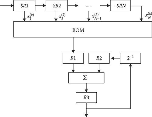
FIGURE 2.9 Processor specifically designed: SR, the shift register; and R, the register.
Pulse packet of the target return signals is shifted by turns at the shift registers SR1, …, SRN starting from the low-order bit. At first, the values X(n−1)i at the output of each shift register are used for addressing the corresponding value of the function Gn−1(X(k)1,X(k)2,…,X(k)N) from ROM. This value is loaded in the register R1 and added to the register R2 content (zero content at the first step). The obtained result is recorded by the register R3. At the next cycle, the value of the function Gn−2(X(k)1,X(k)2,…,X(k)N) is chosen and the content of the register R3 (the previous sum) is recorded by the register R2, with the right shift on one bit that corresponds to multiplication on the factor 0.5. The content of the register. R1, that is, the value of the function Gn−2(X(k)1,X(k)2,…,X(k)N), is added to the content of the register R2 that is a value of the function 0.5Gn−1(X(k)1,X(k)2,…,X(k)N). As a result, we obtain a regular particular result. This operation is repeated n times, and in doing so, at the last step, the function G0(X(0)1,X(0)2,…,X(0)N) is subtracted from the accumulated sum and the final result of convolution given by (2.90) is the content of the register R3 after n cycles.
As we can see, a realization of the considered accelerated convolution is not difficult for low values of the sample size N, for example, N = 10…12. With increasing N, the required ROM size becomes very large, for example, at N = 15, QROM = 32798 words, and an access time is increased essentially. We can decrease the ROM size by partitioning a calculation process using a set of steps with later summing up results. Assume N = LM, where M is the number of functions Gk(X(k)1,X(k)2,…,X(k)N) and L is the number of binary arguments of these functions, then, in this case, (2.86) can be written in the following form:
ZoutDGD=L∑i=1(2S*iXi−X2i+ξ2AFi)+2L∑i=L+1(2S*iXi−X2i+ξ2AFi)X2i+…+N∑i=(M−1)(L+1)(2S*iXi−X2i+ξ2AFi).(2.91)
Each individual sum can be determined by the earlier-described procedure. For this case, the ROM size is determined as QROM = 2LM instead of 2N = 2M × 2L without the partition of calculation process.
2.4 Convolution in Frequency Domain
Now, consider the features of discrete convolution in frequency domain. In accordance with the theory of discrete presentation of continuous functions limited by time or frequency, the function X(t) that can be presented by a sequence of readings {X[i]}, i = 0,1, 2, …, n − 1 is transformed in frequency domain by discrete Fourier transform (DFT) that for each k = 0,1, 2,…, n − 1 takes the following form [24]:
FX(k)=n−1∑i=0X[i]exp{−j2πikn}=n−1∑i=0X[i]Wikn,(2.92)
where
Wn=exp{−j2πn},(2.93)
and vice versa, any function presented by the limited discrete spectrum {FX[k]}, k = 0,1,2, …, n − 1, can be reconstructed in the time domain using the inverse discrete Fourier transform (IDFT):
X[i]=1nn−1∑k=0FX[k]exp{j2πkin}=1nn−1∑k=0Fx[k]W−ikn.(2.94)
Note that the number of discrete elements of the function X(t) is the same for its presentation both in the time domain and in the frequency domain.
Convolution of sequences in the frequency domain is reduced to product of DFT results. For this purpose, there is a need to realize two direct Fourier transforms, namely, to convolve a sequence of readings of the function {X[i]}, i = 0, 1, 2,…, n − 1 and a sequence of readings of the impulse response of filters used by DGD. If after convolution it is necessary to make transformations into the time domain, there is a need to carry out IDFT for sequence of spectral components {FX[k]}, k = 0,1, 2, …, n − 1.
For complex functions (signals) an algorithm of the operation DF T-Convolution-IDF T takes the following form:
1. ˙FH[k]=n−1∑i=0˙H[i]Wikn,k=0,1,2,…,n−1,(2.95)
where ˙H[i] is a sequence of readings of the complex impulse response of the convolving filter:
2. ˙FX[k]=l−1∑i=0˙X[i]Wikl,(2.96)
where ˙X[i] is a sequence of complex readings of the input (convolved) function (the target return signal).
3. ˙FZoutDGD[k]=˙FH[k]˙FX[k],k=0,1,…,l+n−1.(2.97)
4. ˙ZoutDGD[i]=1l+nl+n−1∑k=0˙FZoutDGD[k]Wikl+n−1,i=0,1,…,l+n−1.(2.98)
Principal peculiarity of the considered algorithm is a group technology type flow procedure if the width of an input data array is higher n, that is, l > n. The resulting convolution width is l + n − 1. Under solution of detection problems by DGD, we assume that the impulse response of all filters used by DGD is not variable, at least for probing signals of the same kind. Therefore, the DFT of impulse response of all filters used by DGD is carried out in advance and stored in the memory device of the corresponding computer. In the course of convolution, there is a need to accomplish one DFT and one IDFT. It must be emphasized that under radar detection and signal processing problems, a convolved sequence width L corresponds to radar range sweep length that is much more in comparison with the width of convolving sequence equal to the width of an impulse response nim of filters used by DGD. In accordance with Section 2.1, nim = n0, where n0 is the number of discrete elements of the expected target return signal. Synchronous convolution of such sequences is a very cumbersome process. Because of this, as a rule, the input sequence is divided on blocks with the width l. Each element of the p-th block is generated from a general sequence {˙X[i]}, i = 0, 1, 2, …, L following the law
˙Zp[i]=˙Z[i+pl],n=0,1,2,…,In[Ll],(2.99)
where In[L/l] is the integer part of the ratio in brackets.
For each input data block of the width l the (l + n − 1)-point DFT is determined. For convolving sequence of impulse response of filters used by DGD the components of the (l + n − 1)-point DFT must be determined in advance and stored in a memory device. Convolution in frequency domain for each block is obtained by multiplication between the DFT of convolved and convolving sequences at (l + n − 1) points. To determine the convolution in time domain the IDFT is accomplished. The widths of obtained sequence ˙ZoutDGDp[i] are equal to (l + n − 1) and the neighboring sequences ˙ZoutDGDp[i] and ˙ZoutDGDp+1[i] are overlapped at the n − 1 points. Thus, only the l sequence values will be true. Furthermore, the sum of overlapping partial sequences is used to obtain the correct calculation results for ˙ZoutDGD[i] in all points. In the course of design process, the problem of selecting the optimal value l at a fixed n by criterion of minimum convolution time arises. At low values of nim ≤ 100 the condition lopt ≈ 5nim is satisfied [11,21].
Consider now the problem of work content to realize the DGD in frequency domain. DFT or IDFT requires (l + n − 1)2 operations of multiplication and (l + n − 1) operations of summation for complex values to obtain the (l + n − 1) frequency (time) samples. The total number of required operations taking into account transformations from the frequency domain to the time domain after convolution consists of 2(l + n − 1)2 + (l + n − 1) multiplications and 2(l + n − 1) summations for complex values. In doing so, we obtain the sample of the output data with the width l. To obtain the same length for output data in the time domain, l2 operations of multiplications and l − 1 operations of summations are required for complex values. Consequently, a convolution in the frequency domain is more time-consuming compared to a convolution in the time domain, approximately eight times if lopt ≈ nim. Thus, there is no purpose to implement a convolution in the discussed form for DGD.
We can essentially decrease the number of operations at convolution in the frequency domain by employing the specific DFT algorithms that are called the fast FT (FFT) [25]. Now, consider the design principles of the FFT algorithm with time decimation by modulus 2 of real sequence. Let the sequence {X[i]} that is processed by DFT have the width M corresponding to the integer power of the number 2, that is, M = 2m. This initial sequence can be divided into two parts in accordance with the following rule:
Xeven[i]=X[2i]andXold[i]=X[2i+1],i=0,1,…,0.5M.(2.100)
The sequence Xeven[i] consists of elements of the initial sequence with even numbers, and the sequence Xodd[i] consists of elements of the initial sequence with odd numbers. The width of each sequence is equal to 0.5M. The sequences obtained in the issue of expansion are expanded again in two parts, while 0.5M two-point sequences are delivered. The number of expansion steps is equal to m = log2M.
The essence of the FFT algorithm with time decimation by modulus 2 is as follows. The DFT sequences with the width l > 2 are calculated by a combination of DFT of two sequences with the width equal to 0.5 l. In accordance with this fact, at first, the 0.5M-point DFT of two sequences is carried out under processing of the M-point sequence by FFT. Then the obtained transformations are united for the purpose of creating the 0.25M four-point sequences, 0.125M eight-point sequences, and so on, while a transformation of the width M will be obtained after m steps. FFT determination is carried out by the following formulas:
F[k]=Feven[k]+Fodd[k]WkM,k=0,1,…,0.5M−1,(2.101)
F[k+0.5M]=Feven[k]−Fodd[k]WkM,k=0,1,…,0.5M−1,(2.102)
where
Feven[k]=0.5M−1∑i=0Xeven[i]Wik0.5M(2.103)
and
Fodd[k]=0.5M−1∑i=0Xodd[i]Wik0.5M(2.104)
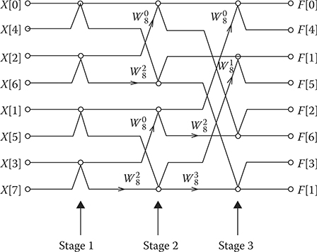
FIGURE 2.10 The directed graph for 8-point FFT.
are DFT for even and odd sequences, correspondingly; WkM=(WM)k is the k-th power of the factor. WM, which is called rotating factor.
Directed graphs are used to represent graphically the FFT algorithm. The following notations are implemented under graphical representations: The point. (or circle) denotes the summation– subtraction operation, the final sum appearing at the top output branch and the final subtraction appearing at the bottom output branch; the arrow on the branch denotes the multiplication by constant written over the arrow; if the arrow is absent the constant factor is equal to unit. The directed graph for 8-point FFT with time decimation by modulus 2 is shown in Figure 2.10. An order of input data assignment is obtained using a procedure of binary inversion of the numbers 0, 1, 2, 7. Such procedure makes a representation simpler and allows us to obtain the input sequence in the natural order—F[0], F[1], F[2], F[3] at the top output branches and F[4], F[5], F[6], F[7] at the bottom output branches. As we can see from Figure 2.10, the 8-point FFT is accomplished over three steps.
At the first step, the four 2-point DFTs are implemented and the condition W2 = exp{-jπ} = −1 is taken into consideration. By this reason, the multiplication operations are absent, and in accordance with (2.98), we can write
F[0]=Feven[0]+Fodd[0]andF[1]=Feven[0]−Fodd[0].(2.105)
At the second step, two pairs of 2-point FFTs are combined with two 4-point FFTs according to (2.101). At the third step, two 4-point FFTs are transformed into the 8-point FFT. In general, the number of steps is defined as m = log2M. At each step, excluding the first step, one half of M multiplications and M summations for complex values are processed. For this reason, to determinate M-point FFT we need (M/2)log2M multiplication operations and M log2M summation operations for complex values.
Previously it was shown that to determine the DFT we need M2 multiplications and M summations for the complex values. The advantage in the number of multiplication operations under realization of FFT in comparison with the direct DFT is
v=M2(M/2)log2M=2Mlog2M.(2.106)
For example, v ≈ 200 at M = 1024, v ≈ 21 at M = 128.
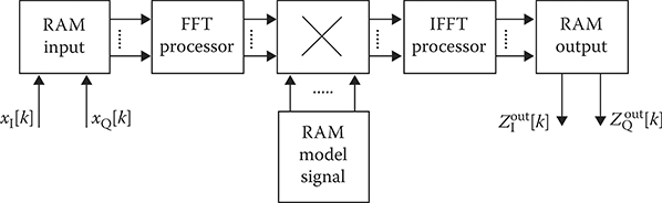
FIGURE 2.11 The FFT-specific processor.
Now, return to the problem of signal processing in frequency domain for DGD taking into account the FFT implementation. A flowchart of the corresponding FFT-specific processor is shown in Figure 2.11. The FFT-specific processor consists of the input memory device, FFT processor, IFFT processor, ROM device, multiplier, and output memory device. As can be seen from Figure 2.11, the in-phase and quadrature constituents of the target return signal come in at the input memory device simultaneously. The in-phase and quadrature constituents of the target return signal form the complex signal subjected to the transformation FFT-Multiplication-IFFT. Because of this, the input and output memory devices and all intermediate registers must possess a double bit width.
For signal processing by the DGD there is a need to carry out the FFT, IFFT, and multiplication between 2 × M-point complex values. Furthermore, we assume that M = l + n − 1. Since the main operation time of the considered specific processor is spent by multiplications between complex and complex conjugate values, the number of convolution operations can be presented in the following form:
Nsp=2[0.5Mlog2M]+m=M[1+log2M].(2.107)
The number of convolution operations for the in-phase and quadrature constituents of one sequence of the output signal is determined by
Nspl=M[l+log2M]l.(2.108)
Under direct calculations in time domain, the number of multiplications between the complex values for a single sample is equal to n at l = n. Consequently, a gain in the number of multiplication operations for complex and complex conjugate values implementing the direct FFT can be determined in the following form:
gFFT=n2M[1+log2M]=n2[1+log22n].(2.109)
Calculations made by this formula show that the gain gFFT > 1 can be obtained only for the case l ≥ 12. Thus, at l = 2048 we obtain gFFT = 85. It can be seen that a greater gain in the number of multiplication operations between the complex and complex conjugate values can be obtained only for high-width sequences.
Now, let us evaluate the required memory size to realize the DGD in radar signal processing subsystem under the implementation of the FFT. Using the same memory storage cells for FFT and IFFT and the buffer to store the output signal (see Figure 2.11), the memory size required for functional DGD purposes is Q = M1 + M2 + M3 + l, where M1 is the number of storage cells required for input sequence sells, M2 is the number of storage cells required for FFT and IFFT, M3 is the number of storage cells required for spectral components of impulse responses of all filters used by DGD, and l is the number of storage cells required for the output sequence. Thus, the use of FFT requires higher memory size in comparison with the implementation of FT in the frequency domain. A frequency of convolution operations can be essentially increased using a continuous-flow FFT system. In this case, the specific processor for FFT consists of 0.5Mlog2 M devices for arithmetic operations functioning in parallel. Each arithmetic device fulfills a transformation at a definite stage of FFT. In doing so, we can reduce the calculation time in log2 0.5M times The continuous-flow FFT system requires additional memory in the form of interstage delay registers.
2.5 Examples of Some DGD Types
At the initial stage of designing, first of all, there is a need to define the following parameters of digital signal processing by DGD: the sampling rate fs and the width of digit capacity of the target return signal amplitude samples Nb. DGD performance and requirements of digital signal processing devices used by DGD depend strongly on a choice of these parameters. Corresponding practical recommendations can be delivered by analyzing different types of DGD designing and construction by computer simulation. In what follows, we present some of the DGD simulation results for chirp-modulated target return signals with the frequency deviation ΔF0 equal to 5MHz.
With the sampling theorem viewpoint, the sampling period Ts of chirp-modulated signals is considered like the limiting case if the following condition T = 1/ΔF0 is satisfied for the in-phase and quadrature channels. The curve 1 in Figure 2.12 corresponds to the DGD output signal at various values Ts in neighboring area relatively to the peak of compressed signal. At Ts = 1/ΔF0 the DGD output signal is represented by a single point in the main lobe area (the point a in Figure 2.12). The main lobe area width near its base is equal to 2/ΔF0.
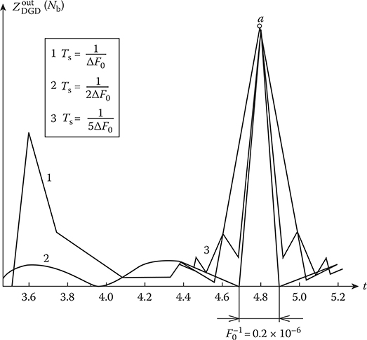
FIGURE 2.12 The DGD output signal amplitude versus the sampling period Ts.
In general, the DGD output signal has big side lobes with amplitudes for about one-half amplitude of the main lobe, which is undesirable. At Ts = 1/2ΔF0, in other words, when the sampling rate is two times higher than the limiting sampling rate fsmax, two readings are within the limits of the main peak with the width equal to 1/ΔF0. At Ts = 1/5ΔF0, the DGD output signal is close to the analog GD output signal. As evident from the simulation results discussed, the sampling rate must be at least two times higher than the limiting sampling rate fsmax. There is a need to take into account the fact that an increase in the sampling rate. fs causes a drastic increase in DGD design and realization complexity, that is, the technical specifications to required performance and memory size of digital signal processing equipment become rigid. For this reason, in the course of designing the DGD, it is recommended to choose the sampling rate fs within the limits 2 ÷ 3ΔF0.
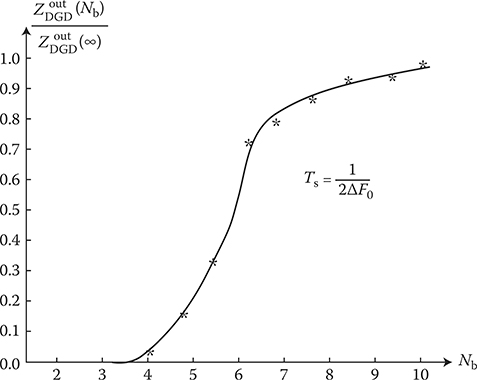
FIGURE 2.13 The DGD output signal amplitude ratio ZoutDGD(Nb)/ZoutDGD(∞) as a function of the digit capacity Nb of input signal.
The number of bits of the sampled target return signal or digit capacity sampling width plays a very important role in the definition of the DGD performance. Computer simulation results representing a DGD output signal amplitude ratio ZoutDGD(Nb)/ZoutDGD(∞) as a function of the digit capacity of the target return signal amplitude samples Nb are shown in Figure 2.13. Here ZoutDGD(Nb) denotes the DGD output signal at limited digit capacity Nb and ZoutDGD(∞) denotes the GD output signal without sampling (Nb → ∞). As we can see from Figure 2.13, at Nb ≥ 10…12 a dependence of the DGD output signal amplitude peak on the digit capacity Nb is weak. Thus, this digit capacity Nb can be recommended under the DGD designing in digital signal processing subsystems of complex radar systems.
2.6 Summary and Discussion
The discussion in this chapter allows us to draw the following conclusions.
Under the designing of analog-to-digital converters, the task of choosing a sampling interval value and the number of signal quantization levels of the sampled target return arises. Simultaneously, we should take into account the problems of designing and realization both for converters and for digital receivers processing the target return signals.
A sampling device can be considered as a make circuit with the time τ and sampling period Ts. The instantaneously sampled target return signal xδ(t) has a mathematical form similar to that of the Fourier transform of a periodic signal. Representation of the continuous function x(t) in the form of the sequence {x(nTs)} is possible only under well-known restrictions. One restriction in kind is a requirement of spectrum limitation of the sampled target return signal xδ(t). By Kotelnikov’s theorem concerning the signal space concept [4], the continuous target return signal x(t) possessing a limited spectrum is completely defined by a countable set of samples spaced Ts ≤ 1/(2fmax) seconds apart, where fmax is the cutoff frequency of target return signal spectrum.
The complex envelope of a narrowband radio signal can be presented either by the envelope and the phase, which are the functions of time, or by the in-phase and quadrature components. Accordingly, under the narrowband radio signal sampling there is a need to use two samples: either the envelope amplitude and the phase or the in-phase and quadrature components of complex amplitude of the narrowband radio signal. Thus, we deal with two-dimensional signal sampling.
Under digital signal processing of target return signals in CRSs there is a need to carry out a quantization of sampled values of complex envelope and phase or in-phase and quadrature components of radio signals in addition to sampling. Devices that carry out this function are called quantizers. We define the main parameters of the analog-to-digital conversion: sampling and quantization errors, reliability, that is, the ability to keep accuracy at given boundaries within the limits of definite time interval under a given environment, and other parameters producing a limitation in power consumption, weight and dimensions of analog-to-digital converters, cost under serial production, time that is required for design, and so on. We would like to pay attention to the following fact that there are two types of sampling and quantization errors: the dynamical errors and statical errors. The dynamical errors are the discrete transform errors. The statical errors are the unit sample errors. The dynamical errors depend on the target return signal nature and time performance of the analog-to-digital converter. The main constituent of this error is an inaccuracy caused by variations in the target return signal parameters at the analog-to-digital converter input.
The sampling and quantization techniques are used to digitize analog signals. For example, the sampling technique is used to discretize a signal within the limits of the time interval, and the quantization technique is used to discretize a signal by amplitude within the limits of the sampling interval. For this reason, there is a need to distinguish errors caused by these two digitizing techniques that allow us to obtain a high accuracy of receiver performance. Amplitude quantization and sampling can be considered as the additional noise ζ1(kTs) and ζ2(kTs) with zero mean and the finite variances σ2ζ1 and σ2ζ2 respectively. If the relationship between the chosen amplitude quantization step Δx and the mean square deviation σ′ of process at sampling, and quantization block output is determined by Δx < σ′, then the absolute value of mutual correlation function between the amplitude quantization error and the signal is approximately equal to 10−9 with respect to the values of the autocorrelation function of the signal. Therefore, it is reasonable to neglect this mutual correlation function. As a first approximation, it is reasonable to assume that the noise ζ1(kTs and ζ2(kTs) are Gaussian.
In the case of the phase-code-manipulated target return signal, the DGD employed by a digital signal processing subsystem in a CRS uses only four convolving blocks. Moreover, a convolution within the limits of each cycle equal to the elementary signal duration τ0 is a summation of amplitude samples of the in-phase and quadrature constituents of the target return signal at instants with signs defined by values S*[i] = ±1 in accordance with the given code of the phase-manipulated operation. Practical realization of this principle is not difficult. In the considered case, a direct realization of convolution operations by serial digital signal processing techniques is not possible. There is a need to apply specific procedures of calculations under digital signal processing. First of all, we may use a principle of parallelism that is characteristic of convolution problems. This principle allows us to calculate n0 of pairwise multiplications S*[i] × x[k − (n0 − i)], where i = 1,…, n0, simultaneously using n0 parallel multipliers with subsequent summation of partial multiplications (see Figure 2.8). In this case, each multiplier must possess the processing speed Vreq = 5 × 10⁶ multiplications per second, that is, one multiplication operation per 40 ns. This processing speed can be easily provided by employing VLSI circuits. Another example of accelerated convolution operation is the implementation of specifically designed processor that uses the ROM blocks to store calculations of bitwise multiplications made before. Factor codes are used as result addresses of these bitwise multiplications.
Convolution of sequences in the frequency domain is reduced to a product of DFT results. For this purpose, there is a need to realize two DFTs, namely, to convolve a sequence of readings of the function {X[i]}, i = 0, 1, 2, …, n − 1 and a sequence of readings of the impulse response of filters used by DGD. If after convolution it is necessary to make transformations into the time domain, there is a need to carry out IDFT for a sequence of spectral components {FX[k]}, k = 0, 1,2, …, n − 1.
The principal peculiarity of the considered algorithm of the operation DF T-Convolution-IDFT is a group technology type flow procedure if a width of input data array is higher n, that is, l ≥ n. The resulting convolution width is l + n − 1. In detection problems solved by DGD, we assume that the impulse response of all filters used by DGD is not variable, at least for probing signals of the same kind. Therefore, the DFT of impulse response of all filters used by DGD is carried out in advance and stored in the memory device of a corresponding computer. In the course of convolution, there is a need to accomplish one DFT and one IDFT. It must be emphasized that under radar detection and signal processing problems, a convolved sequence width L corresponds to radar range sweep length that is greater in comparison with the width of a convolving sequence equal to a width of impulse response nim of filters used by DGD.
Evaluation of the required memory size to realize the DGD in a radar signal processing subsystem under the implementation of FFT is based on the following statements. Using the same memory storage cells for FFT and IFFT and the buffer to store the output signal (see Figure 2.11), the memory size required for functional DGD purposes is Q = M1 + M2 + M3 + l, where M1 is the number of storage cells required for input sequence cells; M2 is the number of storage cells required for FFT and IFFT; M3 is the number of storage cells required for the spectral components of impulse responses of all filters used by DGD; l is the number of storage cells required for the output sequence. Thus, the use of FFT requires higher memory size compared to the implementation of FT in the frequency domain. A frequency of convolution operations can be essentially increased using a continuous-flow FFT system. In this case, the specific processor for FFT consists of 0.5M log2M devices for arithmetic operations functioning in parallel. Each arithmetic device fulfills a transformation at a definite stage of FFT. In doing so, we can reduce the calculation time in log2 0.5M times. The continuous-flow FFT system requires additional memory in the form of interstage delay registers.
References
1. Haykin, S. and M. Mocher. 2007. Introduction to Analog and Digital Communications. 2nd edn. New York: John Wiley & Sons, Inc.
2. Lathi, B.P. 1998. Modern Digital and Analog Communication Systems. 3rd edn. Oxford, U.K.: Oxford University Press.
3. Ziemer, R. and B. Tranter. 2010. Principles of Communications: Systems, Modulation, and Noise. 6th edn. New York: John Wiley & Sons, Inc.
4. Kotel’nikov, V.A. 1959. The Theory of Optimum Noise Immunity. New York: McGraw-Hill, Inc.
5. Manolakis, D.G., Ingle, V.K., and. S.M. Kogon. 2005. Statistical and Adaptive Signal Processing. Norwood, MA: Artech House, Inc.
6. Goldsmith, A. 2005. Wireless Communications. Cambridge, U.K.: Cambridge University Press.
7. Kamen, E.W. and B.S. Heck. 2007. Fundamentals of Signals and Systems. 3rd edn. Upper Saddle River, NJ: Prentice Hall, Inc.
8. Tse, D. and. P. Viswanath. 2005. Fundamentals of Wireless Communications. Cambridge, U.K.: Cambridge University Press.
9. Simon, M.K., Hinedi, S.M., and W.C. Lindsey. 1995. Digital Communication Techniques: Signal Design and Detection. 2nd edn. Upper Saddle River, NJ: Prentice Hall, Inc.
10. Richards, M.A. 2005. Fundamentals of Radar Signal Processing. New York: McGraw-Hill, Inc.
11. Oppenheim, A.V. and R.W. Schafer. 1989. Discrete-Time Signal Processing. New York: Prentice Hall, Inc.
12. Kay, S. 1998. Fundamentals of Statistical Signal Processing: Detection Theory. Upper Saddle River, NJ: Prentice Hall, Inc.
13. Tuzlukov, V. 1998. Signal Processing in Noise: A New Methodology. Minsk, Belarus: IEC.
14. Tuzlukov, V. 2001. Signal Detection Theory. New York: Springer-Verlag, Inc.
15. Tuzlukov, V. 2002. Signal Processing Noise. Boca Raton, FL: CRC Press.
16. Tuzlukov, V. 2005. Signal and Image Processing in Navigational Systems. Boca Raton, FL: CRC Press.
17. Tuzlukov, V. 1998. A new approach to signal detection theory. Digital Signal Processing, 8(3): 166–184.
18. Tuzlukov, V. 2010. Multiuser generalized detector for uniformly quantized synchronous CDMA signals in AWGN noise. Telecommunications Review, 20(5): 836–848.
19. Tuzlukov, V. 2011. Signal processing by generalized receiver in DS-CDMA wireless communication systems with optimal combining and partial cancellation. EURASIP Journal on Advances in Signal Processing, 2011, Article ID 913189: 15, DOI:10.1155/2011/913189.
20. Tuzlukov, V. 2011. Signal processing by generalized receiver in DS-CDMA wireless communication systems with frequency-selective channels. Circuits, Systems, and Signal Processing, 30(6): 1197–1230.
21. Tuzlukov, V. 2011. DS-CDMA downlink systems with fading channel employing the generalized receiver. Digital Signal Processing, 21(6): 725–733.
22. Papoulis, A. and S.U. Pillai. 2001. Probability Random Variables and Stochastic Processes. 4th edn. New York: McGraw-Hill, Inc.
23. Hayes, M.H. 1996. Statistical Digital Signal Processing and Modeling. New York: John Wiley & Sons, Inc.
24. Proakis, J.G. and D.G. Manolakis. 1992. Digital Signal Processing. 2nd edn. New York: Macmillan, Inc.
25. Kammler, D.W. 2000. A First Course in Fourier Analysis. Upper Saddle River, NJ: Prentice Hall, Inc.